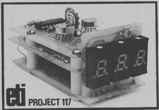
THE three-digit display module described on pages 20-22 is readily adapt able to a wide range of applications. The display module has been designed so that an extra circuit board can be mounted above the display board thus enabling a wide range of additional facilities to be 'in-built'.
In this article we describe a simple yet accurate digital dc voltmeter add on board. It is shown here as a single range unit which is economical enough to be mounted within other equipment as a panel meter. An input switch and scaling resistors could easily be added to convert the instrument for use on ranges from one volt full scale to 1000 volts full scale. We have not described the construct ion of an enclosure as individual requirements will vary widely.
CONSTRUCTION
The display-counter module ETI 533 should be built first using the instructions given on page 20. Two additional boards are required to complete the voltmeter and the overlays and interconnections are given in Fig. 3. Check that all components, especially the metal case ICs are orientated correctly.
The interconnection wires should be long enough to allow the boards to fold together as shown above. The lower board ETI 533A has the components uppermost, the middle board ETI 117A has the components downwards while the top board ETI 117B again has the components uppermost. It may be necessary to juggle the components slightly on the lower two boards to allow them to fit together closely enough. These two boards are spaced apart with 12mm long spacers while the upper two boards are separated by 6mm insulated spacers. A piece of insulation material should be fitted between the top two boards to prevent the solder joints touching.
Power, 9-15 volts dc, is supplied to the lower board while the input connects to the upper board.
The unit can be either installed in a suitable box or within a piece of equipment. If range switches are required simply change the value of R12 as per Table 1. A suitable box for mounting the unit as a separate instrument is the type PC1 marketed by A & R.
CALIBRATION
Unfortunately to calibrate any voltmeter a known voltage reference or an accurate voltmeter is required for comparison. Two adjustments are provided, one for calibration and the other to compensate for the offset in the integrator IC. For input voltages of 10 V or more the offset potentiometer is not required as the error is within one digit.
This offset potentiometer should be adjusted first by applying a voltage of about one percent ( 10 digits) of full scale and adjusting RV2 to give the correct reading. The calibration potentiometer RV1 can now be adjusted by applying an accurately known voltage near full scale.
The meter has a large overrange and voltages up to 250 percent of full scale can be measured except that the first digit is lost and must be assumed, i.e., if you are measuring a car battery on a 10 V range and it reads 3.52 V it is obviously 13.52 V.
---------------
Inexpensive unit uses dual-slope technique.
---------------
MEASURED PERFORMANCE OF PROTOTYPE
Number of digits
Overrange dual polarity Ranges Accuracy Linearity Power supply Input impedance overrange Protection 1 V range 10 V range 100 V range 100 V range 3 250% ( no indication)
No 1, 10, 100 and 1000 V dc
As adjusted
± 1 digit 9-15 V dc at 120 mA isolate( 100 k/V 100 V limited by power 500 V dissipation and 500 V voltage rating of 2500 V* R12
* input switch permitting Reference 5.1 volt zener at constant current.
------------
--------------
HOW IT WORKS
The method of analogue-to-digital conversion used is the popular dual-slope integration technique. We chose the dual-slope technique because it is relatively insensitive to component tolerances and gives very linear results with least mount of circuit complexity. The technique was developed by Weston and hence is covered by patents, however, there is nothing to stop individual constructors from using it, nor are there any royalties involved.
The circuit consists of an integrator (IC4 and C3), a comparator (IC5), an input selector ( IC3), an oscillator (IC6/1,2,3) an RS flip flop (IC7/1,2), pulse generators for the reset and strobe outputs (IC6/4, IC7/3,4), a voltage reference ( ZD1 and constant current source ( QI), and the digital display module on page 74.
The 5 kHz output of the oscillator, which runs continuously, is connected directly to the clock input of the display module and the conversion proceeds as follows. Flip Flop 1C7/2, drives IC3 such that it selects either the input voltage via R12 or the reference voltage via R13.
The state of the flip flop is determined by the output state of the comparator ICS (output high selects input voltage) and the overflow output from the display module (overflow selects reference voltage). If the input voltage is selected the output of the integrator will fall at a rate dependant on the input voltage, and, if the reference voltage is selected the input voltage will rise at a constant rate.
When the integrator output rises above 5.1 volts the comparator output goes high causing the output of IC6/4 to go low (as pin 5 of IC6/4 is also high). After about 10 µseconds delay, due to R16 and C1, the flip-flop changes state and the output of IC6/4 goes high again Thus a pulse is generated which is used as the strobe to transfer whatever number is in the decade counters into the store, and hence, to the display. The strobe pulse also triggers a 15 microsecond monostable, IC7/3, the output of which is delayed by 10 microseconds and inverted by IC7/4. This new pulse acts as a reset pulse for the counters setting them to zero.
As the flip flop has now reverted to its original state the input voltage is reselected and the integrator commences to ramp down again repeating the cycle.
Whilst the input voltage is selected clock pulses are gated into the counter and after about 200 milliseconds ( 1000 clock pulses each 0.2 mS) the counter will be full. The overflow thus generated from the display changes the state of the flip flop and the reference voltage is selected. The voltage across the integrator ( referenced to 5.1 volts) at this instant will be proportional to the input voltage. With the reference supply connected the output of the integrator will rise at a predetermined rate and on crossing the 5.1 volt reference level the strobe and reset pulses are generated, the flip flop toggled and the process started again.
The time taken to bring the integrator back to the reference level is proportional to the input voltage and hence the number in the decade counter at that instant is the required reading of input voltage.
The only components which are required to have good stability, if accuracy is to be maintained, are R12, R13 and ZD1. All other components, provided their short-term stability is good, can be almost any tolerance. The integrator capacitor, for example, can have any value between 0.5 microfarad and 2.0 microfarads without affecting accuracy. However variations in the value of this capacitor will affect the over-range capability. The clock frequency may likewise be altered without affecting accuracy however, if the time of 1000 clock pulses is a multiple of 20 milliseconds the voltmeter will automatically reject 50 Hz ripple on the voltage being measured. This however was not considered of great enough importance to warrant special adjustment of the clock frequency which is preset by R15 and C4.
The reference supply is a 5.1 volt zener diode and a FET connected as a constant current source. The 5.1 volts is used as the common and hence, the 12 volt supply for the voltmeter must be left floating and must not be connected to ground or to any other equipment.
Due to the simplicity of the circuit there are some features of the instrument which are not desirable but do not greatly affect the operation of the instrument. Firstly there is no over-range indication and thus if 15 volts is applied to the 10 volt range the instrument will read 5 volts. The unit remains accurate (except for the first digit which is lost) until the integrator clips on its negative swing (about 250% of full scale). The other point is that if the input voltage is negative the comparator, IC5, will remain high and no further strobe or reset pulses will be generated. The effect of this is to freeze the display at the last number. This is not normally a problem as the display goes to zero if the input is disconnected.
---------------------
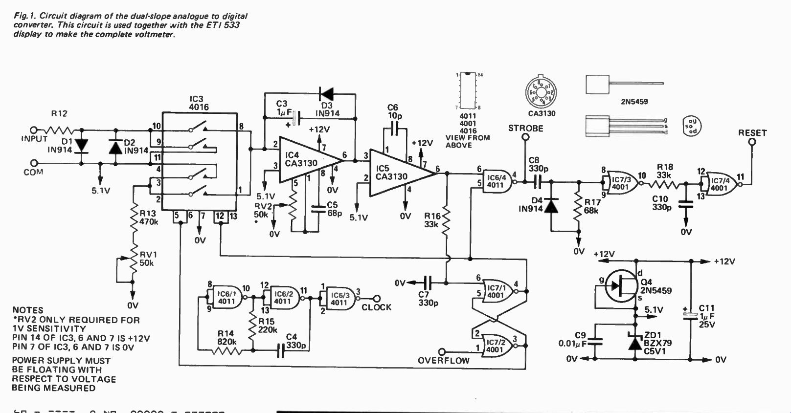
Fig. 1
------------
------------
PARTS LIST
R16,18 R17 R15 R13 R14 R12
Resistor 33k 1 / 4 w 5% 68k" " 220k " 470k 820k" "
See text
RV1,2
Potentiometer 50k Trim type C6
Capacitor 10oF ceramic C5 68 pF " C4,7,8,10 330pF" C9 ,, 0.01uF polyester C3,11 ., 1 p .F 25V Tantalum
D1,2,3 Diode IN914 or similar ZD1 Zener diode BZ x 79 C5 VI Gll
Transistor 2N5459 or similar IC3 Integrated circuit 4016 ( CMOS) IC6 4011 (CMOS) PI IC7 4001 (CMOS) IC4,5 I. It CA3130
PC Boards ETI 117A, ETI 117B
Display Board Complete - Project ETI 533 July 1975
---------------------
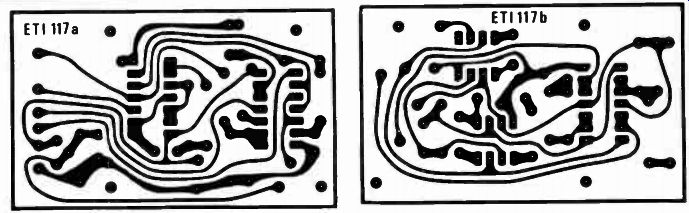
Fig.2. Circuit boards used for the converter.
------------
TABLE 1 RANGE VALUE OF R12 1V 100k 5%* 10V 1M 5%* 100V 10M 5%• 1000V 100M 5%• (10 x 10M) For multirange meters R12 must be 1% or adjustable.
-----------
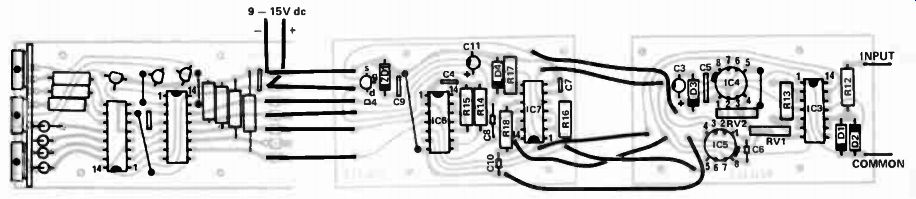
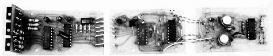
Fig. 3. Component overlay of the complete voltmeter.
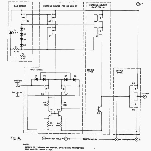
Fig. A. OFFSET NULL COMPENSATION NOTE DIODES DS THROUGH DO PROVIDE
GATE- OXIDE PROTECTION FOR MOS/FET INPUT STAGE
NOTE : The MC14553 is manufactured by Motorola and distributed by Total Electronics. The MC14511, MC14016, MC14011 and MC14001 are also distributed by Total. However these latter devices are also available from other manufacturers under the numbers 4511, 4016, 4011 and 4001 respectively.
Distributors of these latter devices are Cerna, National and AWA ( RCA).
THE CA3130 OPERATIONAL AMPLIFIER
For those unfamiliar with this IC we have reproduced the internal circuitry n Fig. A. It is an economical FET input operational amplifier. This IC is unusual as it combines a FET input tage with a bipolar amplifier and a CMOS output stage, all on the one hip! It is a pin for pin equivalent for he 301/741 type of IC and needs a 68 pF capacitor between pins one and light for compensation. The major differences are a maximum voltage of 6 V between the supply rails (± 8 V) nd the extremely high input resistance of 1.5 T-ohm ( 1 500 000 m-ohm) nd low input current of 5 pA.
--------------------