(source: Electronics World, Aug. 1963)
By HAROLD S. RENNE
New solid-state transducers that detect and measure movement of beam or rod with far greater sensitivity than previously possible with resistance-wire gages.
SEMICONDUCTOR materials have been invading more and more fields. They are used in transistors, solar batteries, diodes, radiation detectors, and thermometers--and now they have invaded the strain-gage field, in a big way. As we will see later, they add a new dimension to the usefulness of strain gages and introduce orders of magnitude of improvement in their operation.
What Is a Strain Gage?
A strain gage is a device for detecting and measuring movement of a beam or rod on which it is mounted. This movement can be the result of tension, compression, bending, twisting, or any other motion that it is desired to measure.
A typical application is to determine the amount of load on a beam by measuring how much it bends. With proper calibration, this load can be calculated very precisely.
Conventional strain gages are made of wire or foil. The wire of the gage is looped back and forth to produce the desired resistance, as shown schematically in Fig. 1. The gage is then bonded to the beam under test by means of a special adhesive. If the beam is bent so that the gage is compressed, the resistance decreases, as the cross-section of the wire increases. If the gage is stretched, the cross-section decreases and the resistance increases.
Gages of this type have been employed for years and they are extremely useful. However, there is one disadvantage to such a device. It is not very sensitive, that is, the change in resistance is very small for moderate strains. The sensitivity is usually indicated by a term called the "gage factor," G, which is a measure of the fractional change in resistance with strain. In most commonly used wire gages, a gage factor of two to four is obtained. The equation for the gage factor may be expressed as follows: G = tSR /RS where DR is the change in resistance, R is the original resistance, and S is the strain (which is also referred to as the change in the length per unit of length).
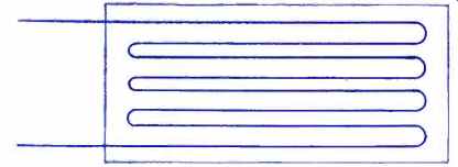
Fig. 1. Wire in a strain gage is looped back and forth in order to produce
desired resistance change when it is bent.
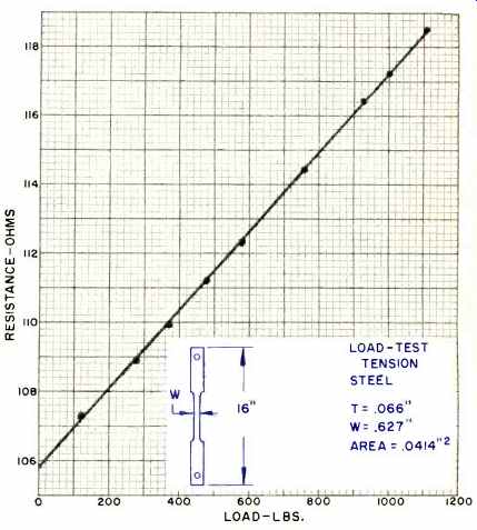
Fig. 2. Resistance-load characteristics of gage mounted on steel.
Early Work with Semiconductors
A few years back, scientists at Bell Telephone Laboratories began a study of the piezoresistive properties of semiconductor materials. The term "piezoresistive" refers to a change in resistance with mechanical deformation. They found that bars of silicon and germanium exhibited changes in resistance far greater than other materials when mechanically deformed by compression or tension. This led to further exploratory work on these materials to determine their suitability for strain gages. Results were extremely favorable.
Early experiments showed that strain gages fabricated of properly doped semiconductor materials could have gage factors as large as 150 to 200, nearly two orders of magnitude greater than wire gages. This work at Bell Labs led to the development of commercial semiconductor strain gages by a number of manufacturers.
Both silicon and germanium have proved to be useful materials for strain gages. In general, silicon has a somewhat higher gage factor and can be used at a much higher temperature than germanium, and so is used most widely. Doping can be either p-type or n-type, and can be either heavy or light, depending on the desired characteristics. Heavy doping reduces the resistance and alters the sensitivity somewhat.
Semiconductor Gage Characteristics
Semiconductor strain gages are usually designed to have the same resistance as standard wire gages, such as the Baldwin-Lima-Hamilton SR-4. Standard resistances are 50, 120, and 300 ohms, but much higher resistance units can be fabricated if desired. The gage is usually made in the form of a bar or strip cut from a properly doped single crystal.
The bar or strip must be oriented properly with respect to the crystalline structure of the single crystal, as the piezoresistive properties are maximum for only certain directions.
Units having the same dimensions can be made with resistances from a few ohms to several megohms by adjusting the doping during crystal growth. Leads must be attached carefully to avoid the formation of rectifying junctions.
Semiconductor strain gages, particularly those made of silicon, have other desirable properties besides high sensitivity. They exhibit very low hysteresis loss. This means that their characteristics are highly reproducible whether a particular point is reached by increasing the strain from a low value, or decreasing it from a high value. The material is quite rugged when properly prepared and is very elastic.
Hence, it can be deformed to quite a degree and will return to its original state when the deforming forces are removed without acquiring any permanent "set." The frequency response is very high, on the order of kilomegacycles, and in general is limited by the external circuitry. There is one disadvantage, however. Both the gage factor and the actual resistance are extremely temperature-sensitive, but there are several ways of compensating for this effect.
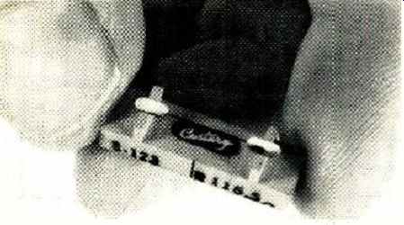
Fig. 3. Typical commercial silicon strain gage in its holder.
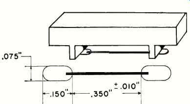
Fig. 4. Dimensions of the strain gage that is shown in Fig. 3.
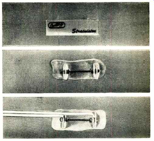
Fig. 5. (A) Gage is first forced by its holder into adhesive on prepared
surface. (B) Holder is removed. (C) The leads are attached. Unit is ready
for use as soon as adhesive has cured.
Great care must be exercised in bonding semiconductor strain gages to the surface on which they are mounted so that there is no slippage or creep. A number of cements are satisfactory if used according to directions. Some require curing at elevated temperatures which may introduce a permanent compression or stretching because of the unequal coefficients of expansion of the gage material and the surface on which it is mounted. This permanent "set" can be used to advantage in some applications. Typical cements that are used include Eastman 910, EPY-150, Mithra #200, and others.
Linearity of silicon strain gages is very good--particularly for the lower-resistance units. A typical curve is shown in Fig. 2, which is a plot of the load in pounds on a steel bar vs the resistance of a Century Electronics' semiconductor strain gage mounted on the bar.
Commercial Semiconductor Strain Gages
As mentioned previously, semiconductor strain gages are commercially available from a number of companies. A few typical units will be described, but it should be understood that this listing is by no means comprehensive.
Fig. 3 shows a silicon strain gage manufactured by the Century Electronics Co. of Tulsa, Oklahoma, and trade--named the "Strainistor." A dimensional diagram of this unit is shown in Fig. 4. This "Strainistor" can be used at temperatures up to 700 °F and at strains of greater than 2000 micro-inches per inch. The gage factor at 72 °F for a 120-ohm unit is from 120 to 140.
The "Strainistor" is supplied on a combination handling and mounting fixture. The series of photos in Fig. 5 shows how the "Strainistor" is mounted on the prepared surface by first embedding it in the cement with which the surface has been coated, then removing the fixture, and finally attaching the leads.
It is possible to use a strain gage to measure pressure.
Fig. 6 shows a gage designed for such a purpose. This particular unit can be used with most gases and liquids and is available in ranges from 25 to 10,000 pounds-per –square-inch. Linearity is very good and hysteresis is negligible. The output is compensated to 3% maximum change over a temperature range of 0 °F to 250 °F.
The Baldwin-Lima-Hamilton Company of Waltham, Mass., a major manufacturer of wire and foil-type gages, also makes a line of silicon gages. These units have an active length of about 0.18 inch, a resistance of 120 or 350 ohms as desired, and a gage factor of 120. Photographs of typical units are shown in Figs. 7 and 8.
Another major manufacturer of semiconductor strain gages is the Kulite-Bytrex Corp. of Newton, Mass. The active element in this company's line is a filament of silicon having a cross-section of about 1 by 5 mils and an effective gage length of ;á inch (dimension B of Fig. 9) , An interesting sidelight is that units are available with a negative gage factor of as high as 140. This means that the resistance decreases with tension and increases with compression.
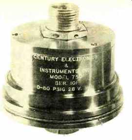
Fig. 6. Pressure transducer with silicon gage active element.
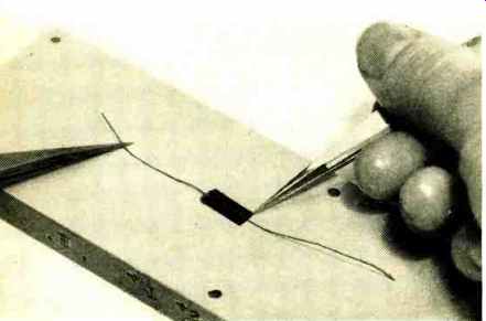
Fig. 7. This silicon strain gage has an active length of 0.18 ".
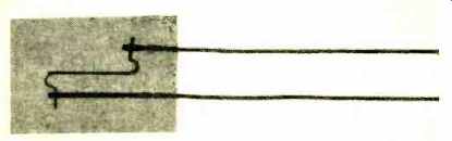
Fig. 8. A different lead configuration is used in this gage.
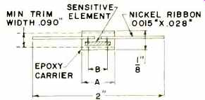
Fig. 9. Dimensions of Kulite-Bytrex silicon strain gages. The dimensions
A and B are typically 1/2 and 1/4 inch respectively.
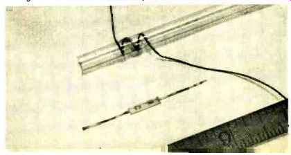
Fig. 10. Photo shows flexibility and small size of Kulite gage.
Kulite-Bytrex lists a number of interesting applications for its strain-gage transducer systems. Some of these are: the automatic weighing of pipe in a tube mill ( Fig. 10) , monitoring the weight change of a bedridden patient, control of screw-down pressure on a 5,000,000-pound rolling mill, and measuring the six components of reaction force of a ballistic missile during captive firing.
Measuring Resistance Change
For a strain gage to be useful, it must be teamed with instrumentation capable of measuring the change in resistance that takes place when the gage is undergoing strain.
Two methods are in general use: the Wheatstone-bridge technique and the voltage-drop technique.
If a strain gage forms one arm of a Wheatstone bridge, the bridge can be balanced for the initial conditions and then any deflection of the gage, resulting in a change in resistance, will produce an indication on the null detector. This detector can be a meter calibrated directly in units of strain. Such a circuit is shown in Fig. 11. It is interesting to note that one, two, or all four arms of the bridge may be made up of active gages.
If current is passed through a gage, a voltage drop will appear across it. Any change in the resistance of the gage resulting from applied strain will change this voltage drop.
By balancing out the original voltage, a voltmeter may be employed to read only the voltage resulting from the change in resistance, and this can be calibrated directly in units of strain. Care must be taken to avoid excessive current through the gage, as it might result in overheating. The manufacturer usually specifies the maximum current--a figure of 30 ma is fairly typical.
Temperature Compensation
As mentioned previously, the electrical properties of semiconductor materials are extremely sensitive to temperature changes. However, several techniques are available for minimizing or eliminating temperature effects in such gages.
Tiny thermocouples, which can be used to determine the exact temperature at the gage at all times, are available.
Then, by means of a calibration chart, the necessary correction for the specific temperature can be determined and the meter reading adjusted accordingly.
In most applications, the temperature coefficient of expansion of the gage is different from the material on which it is mounted. Thus, if the temperature changes during a typical run, this difference in expansion can introduce a considerable error. A very good technique for compensating for this effect is to mount a dummy gage next to the active gage in such a position that it does not undergo strain, but is maintained at the same temperatures as the active gage. The output of this dummy gage can then be used to cancel out the apparent strain due to temperature change.
Another method for temperature compensation is to select two gages with the same temperature coefficient of resistance but with opposite gage factors. This will compensate for the resistance change and, in addition, will provide two active adjacent arms of the bridge. The Kulite-Bytrex Corp. produces such a gage, a cross-sectional view of which is shown in Fig. 12.
Gage factors in excess of 200 can be achieved with this configuration. This same company also makes a transducer gage in which the thermal coefficient is very nearly the negative reciprocal of the thermal coefficient of the modulus of steel. Thus, when bonded to steel, the gage is automatically compensated for thermal effects on sensitivity. This feature, together with a high degree of linearity, results in an extremely useful device.
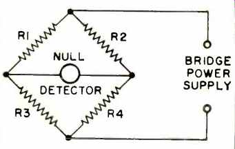
Fig. 11. Wheatstone-bridge configuration.
One, two or all four arms may be gages.
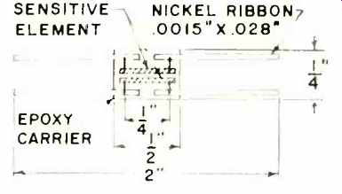
Fig. 12. This unit is automatically compensated for any changes in temperature.
Any article on the subject of semiconductor strain gages would be incomplete without some mention of recent work at Bell Laboratories on the use of semiconductor devices as pressure transducers.
In one device, the positive- and negative-resistance characteristics inherent in a thin p-n junction, such as in an Esaki diode, are modulated. By properly constructing the diode and coupling the desired mechanical motion to the junction, a pressure multiplication factor of as much as a million can be obtained.
Also, by utilizing the negative-resistance portion of the Esaki diode, together with a suitable value of input current and parallel resistance, gage factors as high as 30,000 may be obtained.
Semiconductor materials have made great inroads into the fields of strain and pressure measurements. Research and development are continuing and further new developments are on the way.