(source: Electronics World, Dec. 1963)
By CARL DAVID TODD / Head of Engineering, Modular Circuits, Hughes Aircraft Co.
Here are several ways to check leakage, gain, saturation, and breakdown voltages with equipment normally at hand in the average laboratory.
HOW many times have you wished you could perform a few basic tests on a transistor or diode? Perhaps you wanted to make sure that it was still good after that test, or maybe you wanted to know the value of some critical parameter. While there are several different types of simple testers on the market, it may be that the amount of testing that you do does not justify their purchase. This is particularly true where measurement of the relatively low leakage currents of silicon transistors and diodes is concerned.
In some cases, it is desirable to perform a few basic tests on all transistors and diodes to be installed in a piece of equipment. There may be quite a few units that you would like to test in a minimum amount of time, but you cannot purchase an automatic test set to satisfy your temporary requirement.
This article discusses several ways in which parameters such as leakage currents. d.c. current gain, saturation voltage, and breakdown voltages may be measured with equipment normally on hand in the average electronics laboratory. In spite of the basic simplicity of the tests, the accuracies obtained are usually more than adequate. Some of the tests will be of the go /no-go type while others will yield quantitative results. Both tests are equally simple to make.
Leakage Currents
Let us first consider the measurement of leakage current since this one parameter is perhaps the most revealing with regard to damage or deterioration. A voltage is applied to two of the terminals and the resulting current is measured.
One approach which gives a quantitative result is shown in Fig. 1A. Voltage source El represents the required test voltage to be applied between the collector and base terminals ( for the case for /rum as shown). Actually, E1 should be set to about 0.7 v. higher than the required test value to allow some drop across the current meter. A v.t.v.m. may be used to measure current by placing a shunting resistor across its terminals as shown. For example: R1 of 1000 ohms would give a full-scale current of 1.5 ma ( using the 1.5-v. scale on the meter) . Full-scale currents of 150 pa. and 15 pa. may be obtained using values of R1 of 10,000 and 100,000 ohms respectively.
As we increase the sensitivity to 1.5 pa and 150 nano-amperes (na.) , we must also include the input resistance of the v.t.v.m. ( usually around 11 megohms) when we determine the value of R1.
Thus, for 1.5 pa. full-scale, R1 should be 1.1 megohm and for 150 na. R1 should be 110 megohms ( made up of five 22megohm resistors in series). Since the value of leakage current varies about 10 percent per degree centigrade, it serves little purpose to have a very accurate means of measurement and the approach described above yields adequate results. The actual test voltage will vary somewhat depending upon the voltage drop across the v.t.v.m.; however, this variation is normally small in comparison to the specified test voltage and hence contributes negligible error.
In the case of severe overload, that is, if the leakage current is quite a bit higher than expected, neither the transistor nor the meter will be damaged since the usual v.t.v.m. is capable of standing rather high overvoltages without harm and the measurement resistor serves to limit the current flow through the device under test.
Where many transistors or diodes must be tested on a go /no-go basis to a given specification, it is possible to use a different arrangement which yields a minimum amount of operator decision and hence requires much less test time. The over-all reliability of the test results is also increased.
Fig. 1B illustrates the basic leakage current measurement where a go /no-go test result is required. Voltage supply E1 provides the required test voltage across the collector-base diode (for the I_CBO case shown) . Another voltage source, E2, in conjunction with resistor R1 produces a reference current which is made equal to the current test limit. The voltage across the d.c. null detector is assumed to be insignificant with respect to the voltages E1 and E2. The value of R1 required is E2 divided by the limit test current.
The current flowing into the d.c. null detector is the net difference between the unknown current, Ix (which for the example shown is /rum ) and Is, the reference current. Thus, as long as Le is less than the test limit, the net current, Is. flowing into the null detector will be negative. However, as the value of I_v is increased, the net current approaches zero until I_x is exactly equal to the set limit current. Above this value, the net current into the null detector becomes positive.
Using the go /no-go approach, it is only necessary to note which direction the null detector moves to determine whether the leakage current for the transistor under test is less than or greater than the test limit.
The sensitivity of the null detector required depends on the magnitude of the limit current. For example, the normal v.t.v.m. with 11megohm input resistance and a 1- or 1.5-v. range may be used for test currents down to about 15 na. For lower currents, a d.c. milli voltmeter, such as the Dynamics Model 4472, or a sensitive current meter such as the General Radio Type 1230-A or the Hewlett-Packard Model 4251, may be used. The null detector current sensitivity should be better than one-tenth of the limit current.
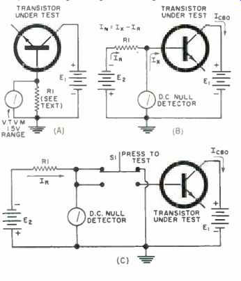
Fig. 1. (Al Basic quantitative leakage current measurements for (B) Basic "go/no-go-leakage
current measurement for ... Improved "go/no-go" leakage current
test.
Using electronic meters, the circuit is capable of withstanding a substantial overload as was true in the previous quantitative measurement. It may be wise to place a momentary switch in series with the unknown leakage current path in such a manner that the null detector is shunted to ground as shown in Fig. 1C. After the transistor is inserted into the socket, switch S1 is depressed and the circuit is as given in Fig. 1B.
The improved circuit has several advantages over the more basic circuit.
First, an overload will normally occur in the meter of Fig. 1B until the transistor is inserted and this may produce an appreciable delay in the reading. The meter of Fig. 1C always starts out from zero such that no overload is present and any zero drift is immediately seen.
Furthermore, any severe overload produced by a faulty component under test will be noticed as soon as S1 is depressed and hence may be removed rapidly (before the meter pins for most cases). Finally, the sensitivity of detection is increased since the operator merely looks for a minor meter movement as a direct result of depressing S1.
The basic circuits of Figs. 1A and 1C may be modified to measure any of the standard leakage currents illustrated in Fig. 2. Although all examples show the testing of an n-p-n transistor, p-n-p transistors may likewise be tested merely by reversing all polarities.
The above circuits may also be used for measuring leakage currents of switches, printed circuits, or ceramic or paper capacitors. Enough time must be allowed to charge the capacitors before such a reading is taken.
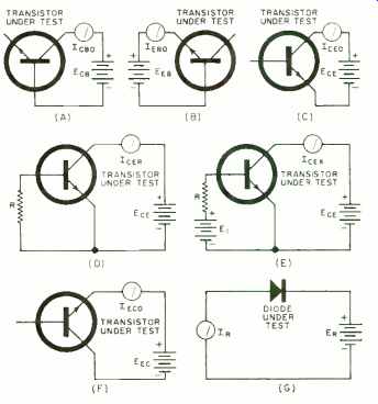
Fig. 2. Simplified measurement circuits are used for various leakage
current parameters.
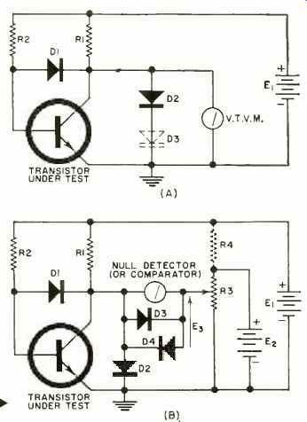
Fig. 3. (Al Quantitative VCE(Rat) measurement. (B) For "go /no-go" VCE(sat)
readings.
Saturation Voltages
Saturation voltage of a transistor is measured with the transistor driven by a constant collector current and a constant base current. The ratio of I_C to I_B is made considerably lower than the natural d.c. current gain of the common emitter stage. In some switching applications, V_CE (SAT) is a very important parameter.
Measuring V_CE (sat) is very simple in its basic form since it is only necessary to provide two current sources with an output voltage variation of only a volt or so. This means that a 100-volt source used with appropriate resistors will yield excellent results. The value of V_CE (sat ) is then the collector-to-emitter voltage under this bias condition.
To prevent the possibility of transistor damage which might result from an increase in power dissipation for a transistor which does not fully saturate, and for operator protection against electrical shock, a sampling arrangement should be used. One complete arrangement is given in Fig. 3A for the quantitative measurement of V_CE(sat).
E1 in conjunction with resistors R1 and R2 provides the two constant-current biases Ic and Ia respectively. The resistor values are determined from the following:
R1 = (E1 –V_CE (sat) Limit)/ I_C = E1 /Ic …. (1)
R2 = (E1 –V_BE) /I_B= (E1- 0.5) /Ia = E1/I_b ….. (2)
Diode D2 serves to limit the collector voltage to about 0.7 v. if a silicon diode is used. Below about 0.5 v., where many saturation voltage measurements are specified, the diode conducts practically no current at all, but as the collector voltage rises above this value, the diode will conduct. For V_CE (sat) measurements above 0.5 v., it may be necessary to add a second diode, D3, in series with D2.
Silicon diode D1 prevents the base from going more positive than the collector by more than 0.7 volt. Since the collector is clamped, then the base will also be held to a voltage of about 1.4 volts or so. In some cases, it may be necessary to use two diodes in place of D1 if the difference between V_BE and V_CE(SAT) should be greater than about 0.5 v.
A test arrangement to yield attribute or go /no-go operation is shown in Fig. 3B. It is the same as the quantitative approach except for a modification in the readout circuitry.
The v.t.v.m. is replaced by a null detector or comparator which is used to compare the actual V_CE (sat) with a reference voltage E3 which is set to the desired rejection limit value.
For value of VCE (sot) exactly equal to the limit value E3, the null detector voltage will be zero. As V_CE (sat) is varied above or below the limit value, the null detector voltage will change from one polarity to another. Using a sensitive null detector, rapid testing of V_CE (sat) may be performed.
Clamping is accomplished as before for the transistor but two germanium diodes, D3 and D4, limit the voltage across the detector when V_CE (sat) is excessively high or very low.
The reference voltage, E3, may be derived from E2 as shown, or from the main supply El as shown by the dotted lines. It should be adjusted with a resistor equal to the ratio of the limit saturation voltage to the value of II, or with the null detector and clamps removed.
The forward voltage of a diode may be measured in a test configuration very similar to that of Fig. 3, with the base current supply and clamping diode removed.
D.C. Current Gain
The d.c. current gain, or more properly, the d.c. current transfer ratio, is another very important parameter not only for d.c. switching and control circuits, but also for the proper biasing of small-signal a.c. circuits. In addition, the a.c. current transfer ratio and its d.c. counterpart have some fair amount of correlation and, since a.c. current gains are more difficult to measure, a simple d.c. measurement may be used to test the transistor. By far the more common parameter is hFE, the d.c. current transfer ratio of the transistor in the common-emitter configuration.
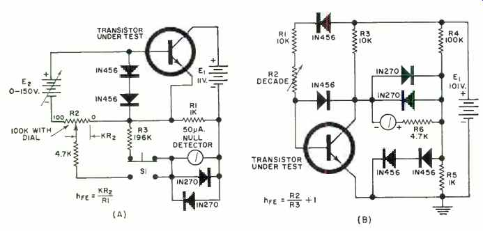
Fig. 4. (A) Simplified quantitative hFE measurement circuit while the
test set circuit of (B) can be used for quantitative or "go /no-go" hFE
live measurements.
By definition hfe is merely the direct ratio of the collector current, Ir, to the base current, In, for a given set of bias conditions (normally a fixed V_CE and I_C). It would, at first thought, seem the natural procedure to set up the bias arrangement and then measure I_C and I_B by means of milli-ammeters and then taking the required ratio. The resulting test accuracy is very poor, and two rather expensive meters are required for precision better than ± 20%. There are several methods that yield much better results with less costly equipment and without the necessary calculations. It is possible to design a production go /no-go arrangement which even eliminates the necessary individual adjustment of the bias. We will now consider several of these approaches.
The simple arrangement of Fig. 4A illustrates a test circuit which will allow the quantitative measurement of hfe. E2 supplies the base current and E1 supplies the bias for the collector circuit. E2 is adjusted until the meter reads full scale. This sets the collector current by using the meter as a voltmeter across R1 and, with E1 set to a constant value, the collector-emitter voltage must also be fixed at a value equal to the difference between El and the measured drop across R1. For the circuit of Fig. 4A, the bias point is 10 ma. collector current and VCE of 1 volt.
Switch S1 is now depressed and potentiometer R2 adjusted until the meter indicates a null or zero-current reading. The value of hfe is then read off the multi-turn dial of R2. This technique is capable of very high accuracy.
A second circuit which may be used for either quantitative or attribute testing of hr is shown in Fig. 4B. A single voltage supply is used with two resistor networks to provide the base and collector currents. The collector current will be determined by the ratio of (E1- V_CE) to R3. The meter acts as a d.c. null detector to compare VCE with a reference voltage determined by voltage divider R4 and R5. The operating conditions for the particular circuit of Fig. 4B are again 10 ma. for I_C and 1 volt for V_CE.
The base current is provided by the resistor network consisting of R1 and R2 and will be equal to (E1- VBE/ (R1 + R2) . For silicon transistors, the value of VBE will be in the neighborhood of 0.8 to 1 volt, or approximately equal to VCE. Under this condition, the value of hFE will be equal to (R1 + R2) /R3 and since R1 and R3 are made equal, hFE is equal to (R2 /R3) + 1. Furthermore, hFE will be directly available from the dial of the decade resistor. A resistance of 100,000 ohms, for example, will indicate an hFE of 10 + 1 or 11. If the resistance required to cause a meter null is 900,000 ohms, then IIPE is 90 + 1 or 91. This circuit has the advantage over the previous one in that the same adjustment that sets the bias condition is also the one that provides the answer. Actually, resistor R1 is not required in the circuit from a theoretical standpoint and, in fact, the readout procedure would be much simpler if it were not present (hFE: would then be merely R2 /R3). R1 has been inserted as a means of protecting the transistor under test, the power supply, and the decade box should the resistance value of R2 accidentally be made too low. It seems much easier to add the extra unit onto the value of hFE than to replace the transistor or decade box.
The circuit of Fig. 4B may be used to provide a quantitative answer of the value of hFE by adjusting R2 until the meter indicates a null or minimum reading, then reading the value of hFE from the dial of R2 (being sure to add the extra 1).
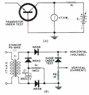
Fig. 5. (A) Measurement of B_VCBO breakdown voltages. (B) Curve tracer
for displaying breakdown voltages on oscilloscope.
The same circuitry may be used as a go /no-go test set by setting R2 to the proper value and then merely noting the position of the meter pointer. If an upscale reading is obtained for the circuit shown, this indicates that the actual value of hFE is higher than the set value.
On the other hand, if the reading is downscale, this indicates that the actual value of hFE is less than the value of the test limit.
A word of caution should be injected here concerning some hFE specifications in which the conditions call for a pulsed measurement. This is a difficult test to perform and while the measurement might be attempted on a straight d.c. basis, we must be absolutely certain that the power rating of the transistor is not exceeded. The value of hFE obtained in the straight d.c. manner will be somewhat higher than that obtained from the pulse measurement.
Breakdown Voltages
Measurement of the various break down voltages of transistors and diodes may be accomplished in one of two ways. A simple voltage supply and meter arrangement, as shown in Fig. 5A, may be used to give approximate results if E1 is very much larger than the breakdown voltage of the transistor under test. Resistor R1 is chosen to limit the maximum amount of current which may flow in the transistor. For many breakdown voltage measurements, particularly for silicon devices, a current level may be varied somewhat without changing the resulting breakdown voltage appreciably.
A second method of measuring the breakdown voltage is by observing the voltage-current electrical characteristics on a curve tracer. Fig. 5B illustrates a very simple circuit which can be used for this purpose. A self-limiting circuit has been included to control the maximum amount of current that may flow. For the circuit values shown, limiting will begin to occur at 150 ua. If R1 is reduced to 100,000 ohms, then limiting will begin to occur at roughly 1.5 ma. The brightness of the trace on the oscilloscope screen will not be uniform because of the nature of the sweep, but an indication of the sharpness of the breakdown characteristic may be observed as well as measuring the breakdown voltage for a given value of current.
Specific breakdown voltages are much like the leakage current parameters indicated in Fig. 2. For example, we might measure BV_CEO by connecting the breakdown measurement terminals between the collector and the emitter, leaving the base terminal open.
In this article, we have considered simple ways to measure several of the more important, or at least more revealing parameters of transistors and diodes. While basic in nature, the techniques presented here yield accuracies equal to or better than many of the much more expensive commercial test sets available and require very little time to set up in the usual electronics laboratory or even service shop. We have not covered every possible detail but information has been presented which, when mixed with a small amount of thought and common sense, will allow valuable quantitative measurements to be taken, the economical testing of semiconductor devices on an incoming inspection basis, or the determination of possible damage to either a transistor or diode.
All of the circuits shown in this article have been bread-boarded and have been used many times with good results.