(source: Electronics World, Mar. 1966)
By JOHN R. COLLINS
This second part of a two-part series covers various types of ultrasonic flaw-detection devices, ultrasonic thickness gages, eddy-current instruments, Hall-effect instruments, and the various types of infrared techniques used in modern NDT tests.
THE increasing interest in non-destructive testing in recent years can be attributed not only to the demand for near-perfect equipment for vital military and space programs, but also to simple economic considerations. Components can be produced more economically if flaws or impurities in materials are detected at an early stage. By locating defective components before they are incorporated into' end products, wasted effort can be eliminated. Finally, a continuing program of equipment overhaul and inspection by non destructive methods can prevent dangerous failures and expensive plant shutdowns.
Much equipment and many techniques have been developed for NDT. Nevertheless, the field is growing. Problems are increasing as fast as solutions. There is every reason to expect that non-destructive testing will become even more important in the years ahead.
Ultrasonic Methods
The use of x-ray apparatus for radiographic and fluoroscopic inspection of materials and components was discussed in Part 1 (February issue ). Although quite effective for many applications, x-rays have notable limitations. Sufficient contrast for good definition is difficult to obtain when small defects are located deep in a metal. Penetrating capabilities are confined, for practical purposes, to several inches of steel.
X-ray equipment for deep penetration ( such as linear accelerators and Van de Graaff generators) is heavy and relatively immobile. It is inconvenient to use for inspecting equipment already installed.
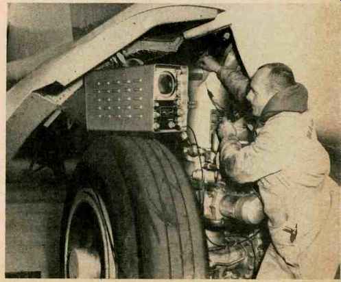
Fig. 1. A portable ultrasonic instrument is used to check an aircraft landing
gear outer cylinder for fatigue cracks.
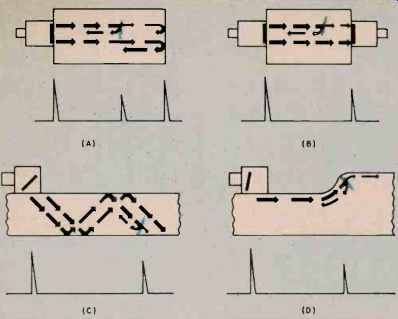
Fig. 2. Four methods of using ultrasonic pulses for flaw detection. (A)
Longitudinal waves. (B) Two-transducer through transmission. (C) Transverse
or shear waves. (D) Surface waves.
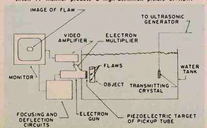
Fig. 3. Special TV camera-like image converter and closed circuit TV monitor
produce a high-definition picture of flaw.
These limitations are largely overcome through the use of ultrasonic testing methods. Mechanical vibrations at frequencies above the audible range can readily penetrate beams 40 feet long without severe attenuation. By using very short wavelengths, small defects can be detected. Furthermore, light, portable equipment can readily be built which is suit able for field use (Fig. 1).
A typical ultrasonic test instrument uses an oscillator to provide electrical energy which can be adjusted to any frequency in a range between 0.5 mc. and 15 mc., and at a pulse repetition rate ranging from 100 to 5000 pulses per second. This electrical energy is converted to ultrasonic energy by means of a piezoelectric transducer. Vibrations are transmitted through the transducer to the piece to be inspected. Energy reflected back from flaws or discontinuities is converted by the transducer to electrical signals which are displayed on the cathode-ray tube. By studying these re flections, the condition of the test piece can be determined.
Quartz crystals or barium-titanate ceramics are generally used for transducers, since these materials are efficient at converting electrical impulses into mechanical vibrations, and vice versa. Unless good contact is made with the surface of the test piece, most of the ultrasonic energy will be reflected back from the surface and only a small portion will enter the test piece itself. To assure good contact, a couplant such as oil, glycerine, or soap film is normally used.
Effective coupling may also be obtained by immersing the test piece and the transducer in a liquid bath of oil or water.
Since the density of these liquids approaches that of the test piece, there is little tendency for energy to be reflected back from the surface. Immersion techniques are useful in testing materials having irregular shapes or rough surfaces. Crystals for high-frequency use are quite thin, and the immersion method reduces wear on the crystal surface.
The various ways of utilizing ultrasonic energy for flaw detection are illustrated in Fig. 2. Although only direct con tact between the test piece and the transducer is shown, immersion techniques are applicable in each instance. Probably the most common method involves the longitudinal wave which is projected in a straight line through the material, as in Fig. 2A. Pulses will appear on the cathode-ray tube to indicate the points at which energy is reflected: at the contact junction between the transducer and test piece, and at the far side of the test piece. Since these are the two chief reflection points, the pulses will be highest there. If there is any flaw or discontinuity in between, some energy will also be reflected back from it. The height of the reflected pulse provides an indication of the size of the flaw, and its position between the two main pulses indicates its location.
A different longitudinal wave method is shown in Fig. 2B.
Two transducers are located on opposite sides of the test piece. Ultrasonic waves are projected by one transducer and picked up by the second. Both transducers, of course, must be coupled to the test piece so that no air gaps exist. If there is 110 flaw, the received pulse should be the same height as the transmitted pulse. A smaller received pulse indicates the loss of energy due to a discontinuity in the path.
This method has the disadvantage that it does not give an indication of the location of the defect. It is useful, however, for such purposes as determining faulty bonding in laminated structures. One of the most important applications of the through-transmission method is to check the walls of space capsules, which are constructed of honeycomb covered with light sheet metal. It is essential that the bond between the skin and the honeycomb be perfect and that there be no internal flaw at any point. An elaborate test setup has been devised in which two transducers are precisely positioned, one inside and one outside, and move together in a pre arranged program that is controlled by tape, covering the entire surface. The transducers are coupled to the walls by means of jets of water.
Through the use of a special probe in which the crystal is set at an angle of 45° to the surface, transverse or shear waves can be projected into the test piece, as in Fig. 2C.
Ultrasonic energy is reflected from surface to surface and, if it encounters a flaw, some of it is reflected back, showing up as a pip on the cathode-ray tube. This method is useful for testing welds and for subsurface defects. Waves of this kind can probe test specimens of various odd shapes and con figurations. The data may be difficult to interpret, however, and it may be necessary to use other methods to pinpoint the location of a defect' after its presence has been detected.
When the crystal is placed at an angle of 60° or 70° to the horizontal, surface waves may be generated, as in Fig. 2D. In this case, the beam is projected along and slightly below the surface of materials and will follow irregular shapes, reflecting from defects in the usual way. Similar transducers are used to produce so-called Lamb waves in thin materials. Lamb waves resemble ripples that travel down the surface and are reflected back to the transducer. They are especially useful for detecting unbonded areas in thin laminations and are more sensitive than shear waves for detecting very small defects on or near the surface.
For good definition, the wavelength of the ultrasonic pulse should be short compared to the defect. It is important to note that the wavelength at a given frequency does not remain constant for all materials, being far shorter in a dense material, such as lead, than in a light material, such as aluminum.
Because of the number of variables involved, a skilled operator is needed to perform other than routine tests with ultrasonic equipment and to evaluate results. However, ultra sonic methods provide a powerful tool for non-destructive testing and are having a remarkable influence in many fields.
A new approach to ultrasonic non-destructive testing is the "Ultra Scan" system developed by James Electronics, Inc.
Using a special TV camera-like image converter sub merged in a tank of water, the object to be tested is placed in the water between the image converter and a source of ultrasonic waves as shown in Fig. 3.
Unlike the single trace displays commonly found in pulse echo systems, this new system operates with a TV-like raster on a high-resolution, closed-circuit TV monitor.
The object undergoing test can be rotated in all directions to find the physical shape of any defect, its dimensions, and its orientation within the test piece. Strip stock and seam welds can be continuously inspected by moving the material past the transducer. Defects as small as .010-inch can be detected.
The system will operate with living tissue as well as metals and many non-metallic materials such as plastic or rubber.
It also permits examination of porosity in cast parts, laminar flow in fluids, and homogeneity of potted assemblies.
Ultrasonic Thickness Gages
In a different kind of operation, ultrasonic energy is used as an effective device for determining the thickness of materials-not only metals of all kinds but also other solid materials, such as glass, plastics, and hard rubber. For gaging purposes, the instrument is provided with a tuning capacitor which permits the continuous tuning of the oscillator over a wide range. The transducer is placed against the wall of the test object and coupled to it by means of grease or soap in the usual way. When the frequency of the oscillator coincides with the resonant frequency of the test piece, a standing wave is set up, as shown in Fig. 4. This point can be detected by the fact that the transducer draws more energy at resonance. The instrument is calibrated to permit the resonant frequency to be interpreted in terms of sample thickness.
An ultrasonic thickness gage made by Magna flux Corporation is shown in Fig. 5 being used to determine wall thickness of a 36-inch Inconel liner used for wind tunnels. For work of this kind, portability is essential. The instrument will measure thicknesses from 0.025 to 3.0 inches and is accurate to 0.014 inch. Both fiat and curved transducers are available to fit objects of different shapes.
Among the uses for ultrasonic thickness gages are maintenance examinations to find areas of corrosion or wear on tanks, pipes, ship hulls, airplane wing skins, and other structures accessible from one side only. In addition, they are used to check thickness of products during manufacture and to detect core shift in heavy castings.
Eddy-Current Instruments
Most electronics technicians have observed that the effective impedance of a coil carrying a high-frequency current undergoes a change if the coil is brought close to a conductor.
This can be explained by the fact that the magnetic field surrounding the coil induces eddy currents in the conductor, and the magnetic field associated with the eddy currents affects the magnetic field of the coil. The situation is like the influence of a transformer secondary on the primary.
Because eddy currents result in power loss, reduction in the magnetic field, and heating, they are normally considered undesirable and steps are taken to minimize their effect. It is interesting to note, therefore, that a new and important category of NDT instruments utilizes eddy currents to analyze substances and to detect flaws.
The basic theory is not difficult to understand. A coil carrying a high-frequency current is placed close to the part to be inspected, inducing eddy currents which, in turn, reflect energy back to the coil. This affects the current flow through the coil and the voltage across it. Obviously, any thing that affects the induced eddy currents will also affect the reflected energy and the coil voltage.
Eddy currents are affected primarily by the permeability of the test piece and its resistance. Many factors influence permeability and resistivity: flaws, discontinuities, chemical composition, condition of heat treatment, dimensions, temperature, etc. This means that eddy-current instruments can test not only for flaws but also for other factors which may be important for quality-control purposes.
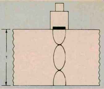
Fig. 4. Measuring material thickness using standing waves.
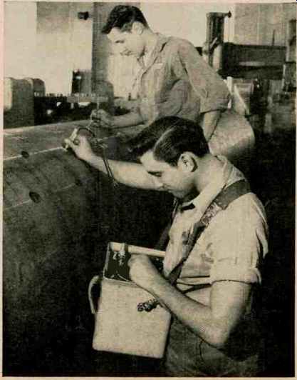
Fig. 5. Portable ultrasonic thickness gage in use. Note the grease couplers
placed at the desired pipe testing locations.
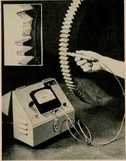
Fig. 6. Test probe locates cracks in a non-magnetic gear.
One of the difficulties is the fact that while a number of variables affect the reflected energy, the information is conveyed only as a change in voltage. It may be difficult, there fore, to determine whether a measured voltage change has resulted from a crack in the test material or, say, a difference in heat treatment or thickness. Elaborate techniques for interpreting the data have therefore been devised. It has been noted that changes in eddy currents resulting from different conditions produce variations in the phase angle of the coil voltage. This can be explained by the fact that currents within a conductor lag surface currents, and a defect at a given depth will result in a phase angle different from that produced by a surface flaw. Conductivity changes affect currents at all depths and result in a different phase angle permeability influence magnetic flux rather than the induced current directly, and since the two are out of phase, still a different phase angle is noted. Changes in dimensions also have a distinct effect.
For analytical work, eddy-current instruments are usually equipped with cathode-ray tubes or some other device for determining the phase angle of the voltage across the coil.
Within limits, it is thus possible to distinguish between flaws at different depths, flaws of different shapes, variations in conductivity, variations in permeability, and differences in dimensions.
Instruments are usually designed to supply any of a number of frequencies to the output coil. For high-conductivity materials, low coil frequencies provide the best separation, and vice versa. Fifty cycles is common for examining ferrous parts, but as low as one cycle may be employed to permit penetration to one-half inch or more in ferrous materials.
Several megacycles may be used for inspection of high-resistivity non-magnetic materials, such as stainless steel, or for measuring very thin plating.
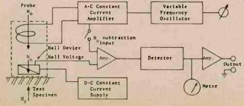
Fig. 7. Hall-effect instrument used in non-destructive tests.
The configuration of the coil depends on the job to be done. An encircling coil is normally used for testing rods or pipe, and inspection is possible at speeds of 300 feet per minute or more. Since any transverse motion of the pipe in the coil would cause a change in the apparent impedance, such movements are rigidly controlled to 0.05 inch or less in any direction from the true center. The system detects scabs, slivers, or other rolled-in materials, open or spotty welds, splits, blisters, etc. A number of different readout devices may be supplied, including a pen recorder and an audible alarm, but the most common device is a paint spray that is triggered by the flaw and marks the defective section of pipe.
A point probe (Fig. 6) is used to inspect material directly under the probe. The instrument shown is compact, operates at a single fixed frequency, and is used to locate and determine the severity of cracks in non-magnetic metals. It may also be used to sort non-magnetic materials according to conductivity or alloy variations and to measure the thickness of both conductive and non-conductive coatings. Special probes are usually designed for particular applications.
Operation is quite simple. The probe is placed on a defect-free test sample, and the balance control is adjusted until the needle of the meter is centered on the scale. As the probe passes over a defect, the needle deflects downscale, and the amount of deflection indicates the severity of the flaw. Coating-thickness measurements and sorting applications are performed in the same way, by recording meter readings on known samples and observing any differences that occur on unknown parts.
Some probes are equipped with differential coils--two coils, side by side, which interrogate adjacent areas on the test piece and provide an output signal equal to the difference between the two voltages. In a differential system, the output is zero when the adjacent areas have the same properties, and an indication appears only when there is a flaw.
Eddy-current testing is comparatively new, and more applications of the technique are constantly being developed.
It has great promise. It permits detection of flaws invisible to the finest x-ray radiography.
It is well-adapted to automatic control.
Hall-Effect Instruments
When a conductor carrying a current is subjected to a magnetic field perpendicular to the direction of current flow, a difference of potential will appear across opposite edges of the conductor. This is known as the Hall-effect. Although the effect is quite small in metallic conductors, voltages that are easily measurable can be produced through the use of flat strips of new semiconductor materials, especially indium arsenide and indium antimonide. If the current through the strip is maintained at a constant level, any change in the measured voltage will be due to a change in the magnetic field. Since a very high degree of sensitivity is possible, Hall-effect devices permit great accuracy in measuring tiny variations in a magnetic field. This factor is extremely valuable in eddy-current testing.
A Hall-effect, eddy-current device called a "Magnetic Reaction Analyzer," made by F. W. Bell, Inc., is shown in the block diagram of Fig. 7. The excitation coil in the probe is supplied by a variable-frequency oscillator, which permits the generation of any frequency from 20 cycles to 100 kc., and a constant-current amplifier which maintains the energizing field Ho at a constant level regardless of the frequency.
When the probe is placed in close proximity to the test object, the Ho field penetrates into the material and generates eddy currents within it. The eddy currents, a function of the material properties, produce a reaction field Hr which adds vectorially to Ho, producing a net field H. at the Hall-effect device (Ho+Hr=Hn.).
The Hall device is mounted in the probe as shown and, when fed from the d.c. constant-current supply, produces a voltage that is proportional to the net field Hn. This voltage is then amplified, detected, and fed to a panel meter for direct reading of the net field Hn. as a percentage of Ho.
The instrument is also equipped to permit a signal proportional to Ho, to be subtracted from the Hall voltage Hn.
The difference is then proportional to H,, thus providing a direct measurement of the reaction field (Ho-Hr=Hn).
Since both Hn and Hr can be read, it is possible to make a complete phase analysis of the eddy-current field.
The fact that the magnetic excitation field is constant at all frequencies permits analysis of ferromagnetic materials at different frequencies under standard conditions, so that comparisons can readily be made of results. The use of a Hall device to detect the magnetic field simplifies phase analysis, extends the usable frequencies to a very low value without loss of sensitivity, and permits deep penetration as well as measurements in very high conductivity materials.
Infrared Techniques
The use of infrared methods for NDT is increasing because some defects can be found faster by infrared applications than by any other method. In other in stances, infrared permits the detection of flaws that cannot be detected by any of the usual testing procedures.
The basic device for infrared testing is the infrared radiometer, an optical instrument which collects radiation within a restricted field of view and converts that energy into an electrical signal. All objects at temperatures above absolute zero radiate energy, most of which is in the infrared region. The wavelength of the radiation is a function of the temperature of the radiator; hence, the electrical signal provided by the radiometer gives an accurate measurement of the temperature of the area surveyed.
Location of imperfect bonding is an almost universal problem because so many laminated materials are now used.
If the surface of a laminated structure is heated, the heat will not be absorbed to the interior as fast at an imperfectly bonded area, and the surface tempera ture will be higher than in surrounding areas. The difference can be detected by scanning the heated surface with a radiometer.
This method is used for testing nuclear fuel elements where proper operation demands a perfect bond between the fuel and the walls of the container.
In practice, the entire surface is scanned by heating a spot on the surface with a torch and rotating the element to permit the spot to be scanned with a radio meter. Hot spots detected in this manner indicate improper bonds.
Infrared scanning can detect poorly soldered or welded connections which exhibit discontinuous thermal conductivity even though electrical conductivity is normal. Fig. 8A shows a thermal scan of a good, 10-watt, wirewound resistor, made with infrared equipment manufactured by Barnes Engineering Company. Note that temperature is highest at the center and decreases in a symmetrical manner towards both ends.
In contrast, Fig. 8B shows a variation in the temperature to the right of center, revealing that the right terminal metal cup is in poor thermal, although perfect electrical, contact. A defect of this particular kind would shorten the life of the unit.
An infrared radiometric microscope, also developed by Barnes, permits the detailed scanning of integrated and thin film circuits. The temperature of each microscopic area is measured and re corded as it is positioned under the cross hairs of the microscope. Any small temperature rise above the ambient may indicate a faulty unit. In the design of monolithic circuits, this permits an ac curate measure of how much power can be dissipated per unit area. During manufacture of microcircuitry, infrared microscopy can detect voids in deposited elements, improper connections, and bonding defects.
Infrared techniques are also adapted to fast checking of crowded printed-circuit boards or components that are in accessible when in operation. By photo graphing a circuit board with an infrared scanning camera, overheated components can be detected within 10 to 60 seconds. The camera incorporates a radiometer which converts the infrared energy into an electrical signal. The electrical signal, in turn, modulates a glow lamp, providing an output in the visible light range which is proportional to temperature. As the surface is scanned, the results are recorded on Polaroid film for a permanent record.
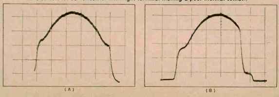
Fig. 8. (A) Thermal scan of good 10-w. resistor shows highest temperature
at the center. (B) Same resistor with right terminal making a poor thermal
contact.