By WALTER W. SCHOPP
Delivers a clean 3.7 watts per channel into 8 ohms without heat sinks or overheated power transistors.
A LOW-wattage amplifier offers some fringe benefits its high-power cousins do not. One is reduced cost of construction. By operating at lower voltages, the cost can be reduced by using lower voltage rated components.
Another benefit is reduced physical size of the components due to the lower working voltages. The smaller capacitors and lower wattage resistors allow construction of a complete two-channel stereo power amplifier on a circuit board measuring only 2 1/4" X 3 1/4 ". This miniature amplifier packs a real punch in the performance department. It will produce a clean 3.7 watts continuous power across an 8-ohm speaker load without heat sinks or overheated output transistors. Its response of 15 Hz to over 30 kHz leaves little to be desired as far as the ear is concerned.
The high input impedance allows the amplifier to be driven directly by a crystal phonograph cartridge if a suitable volume control is added across the input.
By departing from the conventional complementary-symmetry output stage, balancing or biasing diodes are eliminated. The combination of silicon output transistors, Q5 and Q6, with their respective germanium drivers, Q3 and Q4, is unique. With this approach, the output transistors are biased off except for the small base current due to the inherent leakage of the drivers, Q3 and Q4. This allows the drivers to be turned on by very low signal levels without a trace of crossover distortion. The germanium drivers are biased by the voltage drop across resistor R7. This voltage is about half the supply voltage. This configuration is responsible for the extremely low "no-signal" current, which is on the order of 1 to 2 milliamps.
The input stage is "bootstrapped" with the feedback network consisting of resistors R6 and R2 and capacitor C1. This network raises the input impedance to 500,000 ohms.
The components were chosen for their low cost, without sacrificing amplifier performance. They are readily available and no special or hard-to-get items were used. Construction of the amplifier was simplified, and chances of wiring errors reduced, by using an etched-circuit board. Using the components specified in the parts list assures the builder that the circuit board holes will be in the correct places to match the components. The circuit can also be hand-wired in the conventional way as no part of the circuit is critical. The etched, tinned, and drilled circuit board can be purchased (see parts list). After construction, check the voltage on the collector of transistors Q2A and Q2B (Channels A and B). If the amplifier is operating properly, the voltage on these collectors should be half the supply voltage with no input signal to the amplifier.
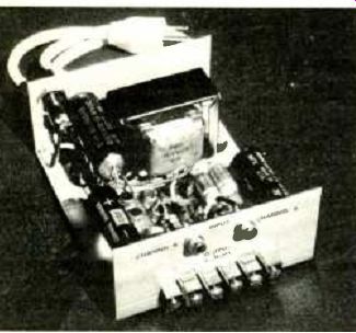
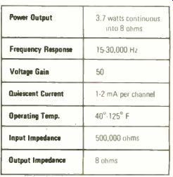
Table 1. Specs of the compact amplifier.
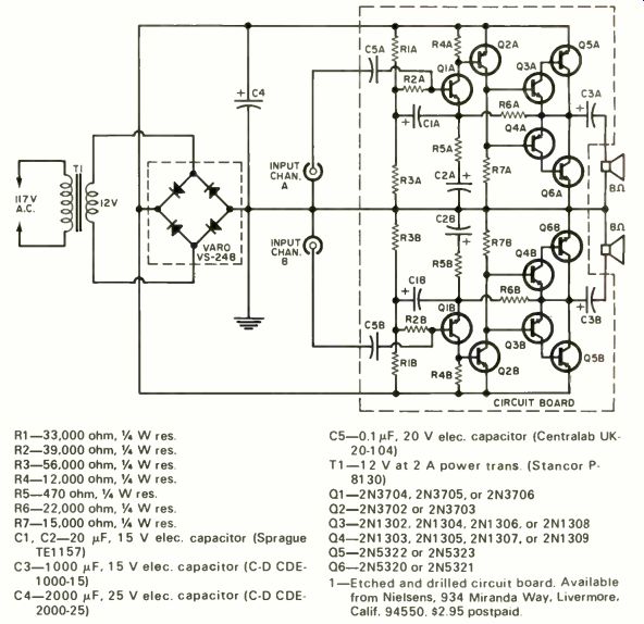
Fig. 1. Complete schematic diagram and parts listing of unit.
R1-33,000 ohm, 1/4 W res.
R2-39,000 ohm, 1/4 W res.
R3-56,000 ohm, 1/4 W res.
R4-12,000 ohm, 1/4 W res.
R5-470 ohm, 1 W res.
R6-22,000 ohm, 1/4 W res.
R7-15,000 ohm, 1/4 W res.
C1, C2-20 uF, 15 V elec. capacitor (Sprague TE1157)
C3-1000 uF, 15 V elec. capacitor (C-D CDE-1000-15)
C4-2000 uF, 25 V elec. capacitor (C-D CDE-2000-25)
C5-0.1 uF, 20 V elec. capacitor (Centralab ÚK-20-104)
T1-12 V at 2 A power trans. (Stancor P-8130)
Q1-2N3704, 2N3705, or 2N3706
Q2-2N3702 or 2N3703
Q3-2N1302, 2N1304, 2N1306, or 2N1308
Q4-2N1303, 2N1305, 2N1307, or 2N1309
Q5-2N5322 or 2N5323
Q6-2N5320 or 2N5321
1-Etched and drilled circuit board.
Available from Nielsens, 934 Miranda Way, Livermore, Calif. 94550.
$2.95 postpaid.
Also see: Link |