AMAZON multi-meters discounts AMAZON oscilloscope discounts
Most stress-related failures are electrothermal in nature. The locally increased temperature can lead to immediate failure by melting or vaporizing metallization layers, melting the semiconductor, or creating other structural changes. The diffusion and electromigration effects tend to be accelerated by high temperature, which shortens the lifetime of the device. Damages to junctions that do not lead to immediate failure manifest as altered current-voltage characteristics of the junctions.
Electrical overstress failures can be classified as thermally induced failures, electromigration related failures, and electric field related failures.
Thermal runaway
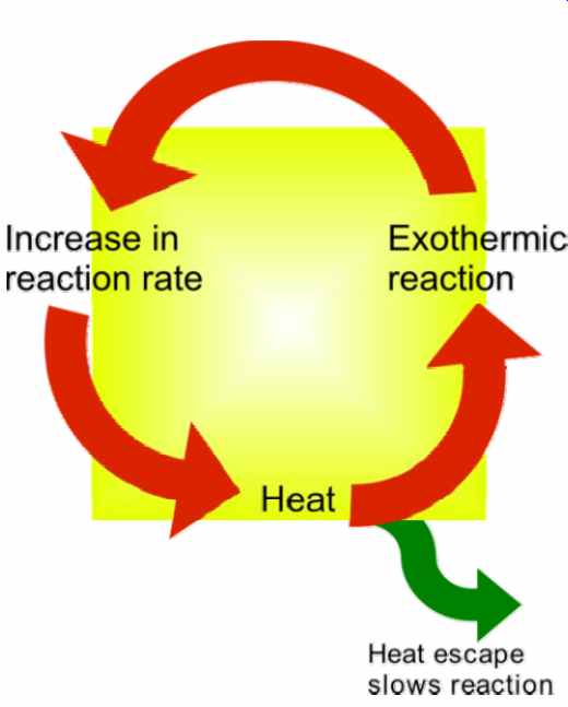
---Diagram of thermal runaway.
Thermal runaway refers to a situation where an increase in temperature changes the conditions in a way that causes a further increase in temperature, leading (in the normal case of an exothermic reaction) to a destructive result. It is a kind of positive feedback.
Chemical engineering
In chemical engineering, thermal runaway is a process by which an exothermic reaction goes out of control, often resulting in an explosion. It is also known as a "runaway reaction" in organic chemistry.
Thermal runaway occurs when the reaction rate increases due to an increase in temperature, causing a further increase in temperature and hence a further increase in the reaction rate. It has contributed to industrial chemical accidents, most notably the 1947 Texas City disaster from overheated ammonium nitrate in a ship's hold, and the disastrous release of a large volume of methyl isocyanate gas from a Union Carbide plant in Bhopal, India in 1984. Thermal runaway is also a concern in hydrocracking, an oil refinery process. Thermal runaway may result from exothermic side reaction(s) that begin at higher temperatures, following an initial accidental overheating of the reaction mixture. This scenario was behind the Seveso disaster, where thermal runaway heated a reaction to temperatures such that in addition to the intended 2,4,5-trichlorophenol, poisonous 2,3,7,8-tetrachlorodibenzo-p-dioxin was also produced, and was vented into the environment after the reactor's rupture disk burst.
Thermal runaway is most often caused by failure of the reactor vessel's cooling system.
Failure of the mixer can result in localized heating, which initiates thermal runaway.
Similarly, in flow reactors, localized insufficient mixing causes hotspots to form, where thermal runaway conditions occur, which causes blowouts of reactor contents and catalysts. Incorrect component installation is also a common cause. Many chemical production facilities are designed with high-volume emergency venting to limit the extent of injury and property damage when such accidents occur.
Some laboratory reactions must be run under extreme cooling, because they are prone to hazardous thermal runaway. For example, in Swern oxidation, the formation of the sulfonium chloride must be performed in a cooled system (-30 °C), because at room temperature the reaction undergoes thermal runaway explosively.
The UK Chemical Reaction Hazards Forum publishes previously unreported chemical accidents to assist the education of the scientific community, with the aim of preventing similar occurrences elsewhere. Almost 150 such reports are available to view at the present time. Microwave heating
Microwaves are used for heating of various materials in cooking and various industrial processes. The rate of heating of the material depends on the energy absorption, which depends on the dielectric constant of the material. The dependence of dielectric constant on temperature varies for different materials; some materials display significant increase with increasing temperature. This behavior, when the material gets exposed to microwaves, leads to selective local overheating, as the warmer areas are better able to accept further energy than the colder areas-potentially dangerous especially for thermal insulators, where the heat exchange between the hot spots and the rest of the material is slow. These materials are called thermal runaway materials. This phenomenon occurs in some ceramics.
Semiconductors
Silicon shows a peculiar instability. Its electrical resistance increases with temperature up to about 160 °C, then starts decreasing, and drops further when the melting point is reached. This leads to thermal runaway phenomena within the semiconductor junction areas; the resistance of the area which becomes hot above this threshold decreases, more of current flows through it causing yet more heating in comparison with the surrounding areas, which leads to further temperature increase and resistance decrease. This leads to the phenomenon of current crowding and formation of current filaments, and is one of the underlying principles behind many semiconductor junction failure mechanisms.
Bipolar transistors
Leakage current increases significantly in bipolar transistors (notably germanium-based bipolar transistors) as they increase in temperature. Depending on the design of the circuit, this increase in leakage current can increase the current flowing through the transistor and with it the power dissipation. This causes a further increase in C-E current.
This is frequently seen in a push-pull stage of a class AB amplifier. If the transistors are biased to have minimal crossover distortion at room temperature, and the biasing is not made temperature dependent, as the temperature rises, both transistors will be increasingly turned on, causing current and power to further increase, eventually destroying one or both devices.
To avoid thermal runaway the operating point of BJT should be Vce = 1/2Vcc The proper practice is to mount a thermal feedback transistor or other device on the heat sink, which generates the crossover bias voltage, so that as the output transistors heat up, so does the thermal feedback transistor, causing the thermal feedback transistor to also start to turn on at a slightly lower voltage, and thus reduce the crossover bias, and reduce the heat released by the output transistors. It can be surprising what professional sound equipment does not have thermal feedback and would thus need modification.
If multiple bipolar transistors are connected in parallel (which is typical in high current applications) one device will enter thermal runaway first, taking the current which originally was distributed across all the devices and exacerbating the problem. This effect is called current hogging. Eventually one of two things will happen, either the circuit will stabilize or the transistor in thermal runaway will be destroyed by the heat. Hence current hogging term is related to thermal runaway.
Power MOSFETs
Power MOSFETs display increase of the on-resistance with temperature. Power dissipated in this resistance causes more heating of the junction, which further increases the junction temperature, in a positive feedback loop. (However, the increase of on resistance with temperature helps balance current across multiple MOSFETs connected in parallel and current hogging does not occur). If the transistor produces more heat than the heatsink can dissipate, the thermal runaway happens and destroys the transistor. This problem can be alleviated to a degree by lowering the thermal resistance between the transistor die and the heatsink.
• Java applet demo of MOSFET thermal runaway
Digital electronics
The leakage currents of transistors increase with temperature. In rare instances, this may lead to thermal runaway in digital electronics. This is not a common problem, since leakage currents make up a small portion of overall power consumption, so the increase in power is fairly modest - for an Athlon 64, the power dissipation increases by about 10% for every 30 degrees Celsius. For a device with a TDP of 100 W, for thermal runaway to occur, the heat sink would have to have a thermal resistivity of over 3 K/W (kelvins per watt), which is about 6 times worse than a stock Athlon 64 heat sink. (A stock Athlon 64 heat sink is rated at 0.34 K/W, although the actual thermal resistance to the environment is somewhat higher, due to the thermal boundary between processor and heatsink, rising temperatures in the case, and other thermal resistances..) A heat sink with a thermal resistance of over 0.5 to 1 K/W would result in the destruction of a 100 W device even without thermal runaway effects.
Electronics and tropical environments Many electronic circuits contain provisions against thermal runaway. This is most often seen in transistor biasing arrangements. However when equipment is used above its designed ambient temperature, thermal runaway can in some cases still occur. This occasionally causes equipment failures in tropical countries, and when air cooling vents are blocked.
Tantalum capacitors
Tantalum capacitors are under some conditions prone to self-destruction by thermal runaway. The capacitor typically consists of a sintered tantalum sponge acting as the anode, a manganese dioxide cathode, and a dielectric layer of tantalum pentoxide created on the tantalum sponge surface by anodizing. The tantalum oxide layer may have weak spots that undergo dielectric breakdown during a voltage spike. The tantalum then comes to direct contact with manganese dioxide and the leakage current causes a local heating; a chemical reaction then produces manganese (III) oxide and regenerates (self-heals) the tantalum oxide layer.
If the energy dissipated at the failure point is high enough, a self-sustaining exothermic reaction may occur, similar to the thermite reaction, with tantalum as fuel and manganese dioxide as oxidizer, destroying the capacitor and occasionally producing smoke and possibly flame.
Batteries
When handled improperly, some rechargeable batteries can experience thermal runaway, resulting in overheating. Sealed cells will sometimes explode. Especially prone to thermal runaway are lithium-ion batteries. Reports of exploding cellphones occasionally appear in newspapers. In 2006, laptop batteries from Apple, HP, Toshiba, Lenovo, Dell and other notebook manufacturers were recalled because of fire and explosions. The Pipeline and Hazardous Materials Safety Administration (PHMSA) of the U.S. Department of Transportation recently established regulations regarding the carrying of certain types of batteries on airplanes because of their instability in certain situations.
This action was partially inspired by a fire on a UPS airplane.
Current crowding
Current crowding (also current crowding effect, or CCE) is a nonhomogenous distribution of current density through a conductor or semiconductor, especially at the vicinity of the contacts and over the PN junctions.
Current crowding is one of the limiting factors of efficiency of light emitting diodes.
Materials with low mobility of charge carriers, eg. AlGaInP, are especially prone to current crowding phenomena. It is a dominant loss mechanisms in some LEDs, where the current densities especially around the P-side contacts reach the part of the emission characteristics with lower brightness/current efficiency. Current crowding can lead to localized overheating and formation of thermal hot spots, in catastrophic cases leading to thermal runaway. Nonhomogenous distribution of current also aggravates electromigration effects and formation of voids. Formation of voids causes localized nonhomogenity of current density, and the increased resistance around the void causes further localized temperature rise, which in turn accelerates the formation of the void. Conversely, localized lowering of current density may lead to deposition of the migrated atoms, leading to further lowering of current density and further deposition of material and formation of hillocks, which may cause short circuits. In large bipolar transistors, the resistance of the base layer influences the distribution of current density through the base region, especially at the emitter side. Current crowding occurs especially at the areas of localized lowered resistance, or in areas where the field strength is concentrated (eg. at the edges of layers).
Reverse bias
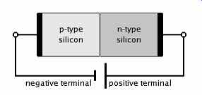
------ A silicon p-n junction in reverse bias.
Reverse biased usually refers to how a diode is used in a circuit. If a diode is reverse biased, the voltage at the cathode is higher than that at the anode. Therefore, no current will flow until the diode breaks down. Connecting the P-type region to the negative terminal of the battery and the N-type region to the positive terminal, corresponds to reverse bias. The connections are illustrated in the following diagram:
Because the p-type material is now connected to the negative terminal of the power supply, the 'holes' in the P-type material are pulled away from the junction, causing the width of the depletion zone to increase. Similarly, because the N-type region is connected to the positive terminal, the electrons will also be pulled away from the junction.
Therefore the depletion region widens, and does so increasingly with increasing reverse bias voltage. This increases the voltage barrier causing a high resistance to the flow of charge carriers thus allowing minimal electric current to cross the p-n junction. The increase in resistance of the p-n junction results in the junction to behave as an insulator.
This is important for radiation detection because if current was able to flow, the charged particles would just dissipate into the material. The reverse bias ensures that charged particles are able to make it to the detector system.
The strength of the depletion zone electric field increases as the reverse-bias voltage increases. Once the electric field intensity increases beyond a critical level, the p-n junction depletion zone breaks-down and current begins to flow, usually by either the Zener or avalanche breakdown processes. Both of these breakdown processes are non destructive and are reversible, so long as the amount of current flowing does not reach levels that cause the semiconductor material to overheat and cause thermal damage.
This effect is used to one's advantage in zener diode regulator circuits. Zener diodes have a certain -- low -- breakdown voltage. A standard value for breakdown voltage is for instance 5.6V. This means that the voltage at the cathode can never be more than 5.6V higher than the voltage at the anode, because the diode will break down - and therefore conduct - if the voltage gets any higher. This effectively regulates the voltage over the diode.
Another application where reverse biased diodes are used is in Varicap diodes. The width of the depletion zone of any diode changes with voltage applied. This varies the capacitance of the diode. For more information, refer to the Varicap article.
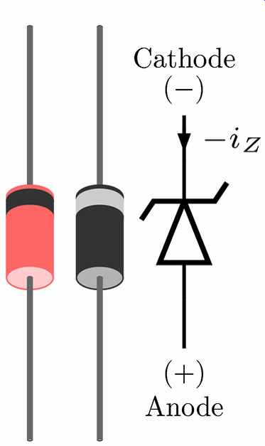
Zener diode
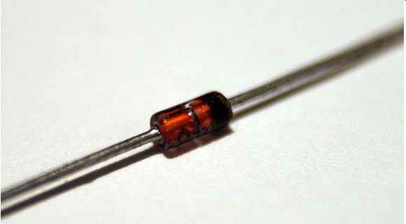
---- Zener diode
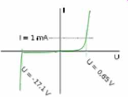
----Current-voltage characteristic of a Zener diode with a breakdown voltage
of 17 volt.
Notice the change of voltage scale between the forward biased (positive) direction and the reverse biased (negative) direction.
A Zener diode is a type of diode that permits current not only in the forward direction like a normal diode, but also in the reverse direction if the voltage is larger than the breakdown voltage known as "Zener knee voltage" or "Zener voltage". The device was named after Clarence Zener, who discovered this electrical property.
A conventional solid-state diode will not allow significant current if it is reverse-biased below its reverse breakdown voltage. When the reverse bias breakdown voltage is exceeded, a conventional diode is subject to high current due to avalanche breakdown.
Unless this current is limited by circuitry, the diode will be permanently damaged. In case of large forward bias (current in the direction of the arrow), the diode exhibits a voltage drop due to its junction built-in voltage and internal resistance. The amount of the voltage drop depends on the semiconductor material and the doping concentrations.
A Zener diode exhibits almost the same properties, except the device is specially designed so as to have a greatly reduced breakdown voltage, the so-called Zener voltage.
By contrast with the conventional device, a reverse-biased Zener diode will exhibit a controlled breakdown and allow the current to keep the voltage across the Zener diode at the Zener voltage. For example, a diode with a Zener breakdown voltage of 3.2 V will exhibit a voltage drop of 3.2 V even if reverse bias voltage applied across it is more than its Zener voltage. The Zener diode is therefore ideal for applications such as the generation of a reference voltage (e.g. for an amplifier stage), or as a voltage stabilizer for low-current applications.
The Zener diode's operation depends on the heavy doping of its p-n junction allowing electrons to tunnel from the valence band of the p-type material to the conduction band of the n-type material. In the atomic scale, this tunneling corresponds to the transport of valence band electrons into the empty conduction band states; as a result of the reduced barrier between these bands and high electric fields that are induced due to the relatively high levels of dopings on both sides. The breakdown voltage can be controlled quite accurately in the doping process. While tolerances within 0.05% are available, the most widely used tolerances are 5% and 10%. Breakdown voltage for commonly available zener diodes can vary widely from 1.2 volts to 200 volts.
Another mechanism that produces a similar effect is the avalanche effect as in the avalanche diode. The two types of diode are in fact constructed the same way and both effects are present in diodes of this type. In silicon diodes up to about 5.6 volts, the Zener effect is the predominant effect and shows a marked negative temperature coefficient.
Above 5.6 volts, the avalanche effect becomes predominant and exhibits a positive temperature coefficient. In a 5.6 V diode, the two effects occur together and their temperature coefficients neatly cancel each other out, thus the 5.6 V diode is the component of choice in temperature-critical applications. Modern manufacturing techniques have produced devices with voltages lower than 5.6 V with negligible temperature coefficients, but as higher voltage devices are encountered, the temperature coefficient rises dramatically. A 75 V diode has 10 times the coefficient of a 12 V diode.
All such diodes, regardless of breakdown voltage, are usually marketed under the umbrella term of "Zener diode".
Uses
-----
Zener diode shown with typical packages. Reverse current - iZ is shown.
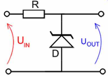
Zener diodes are widely used as voltage references and as shunt regulators to regulate the voltage across small circuits. When connected in parallel with a variable voltage source so that it is reverse biased, a Zener diode conducts when the voltage reaches the diode's reverse breakdown voltage. From that point on, the relatively low impedance of the diode keeps the voltage across the diode at that value.
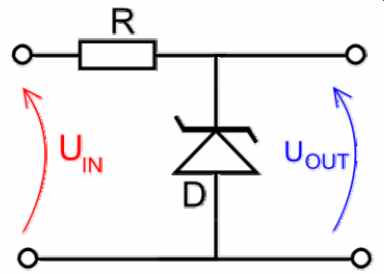
------- In this circuit, a typical voltage reference or regulator, an input
voltage, UIN, is regulated down to a stable output voltage UOUT. The intrinsic
voltage drop of diode D is stable over a wide current range and holds UOUT
relatively constant even though the input voltage may fluctuate over a fairly
wide range. Because of the low impedance of the diode when operated like this,
Resistor R is used to limit current through the circuit.
In the case of this simple reference, the current flowing in the diode is determined using Ohms law and the known voltage drop across the resistor R.
IDiode = (UIN - UOUT) / R_ohm
The value of R must satisfy two conditions:
1. R must be small enough that the current through D keeps D in reverse breakdown.
The value of this current is given in the data sheet for D. For example, the common BZX79C5V6 device, a 5.6 V 0.5 W Zener diode, has a recommended reverse current of 5 mA. If insufficient current exists through D, then UOUT will be unregulated, and less than the nominal breakdown voltage (this differs to voltage regulator tubes where the output voltage will be higher than nominal and could rise as high as UIN). When calculating R, allowance must be made for any current through the external load, not shown in this diagram, connected across UOUT.
2. R must be large enough that the current through D does not destroy the device. If the current through D is ID, its breakdown voltage VB and its maximum power dissipation PMAX, then IDVB < PMAX. A load may be placed across the diode in this reference circuit, and as long as the zener stays in reverse breakdown, the diode will provide a stable voltage source to the load.
Shunt regulators are simple, but the requirements that the ballast resistor be small enough to avoid excessive voltage drop during worst-case operation (low input voltage concurrent with high load current) tends to leave a lot of current flowing in the diode much of the time, making for a fairly wasteful regulator with high quiescent power dissipation, only suitable for smaller loads.
Zener diodes in this configuration are often used as stable references for more advanced voltage regulator circuits.
These devices are also encountered, typically in series with a base-emitter junction, in transistor stages where selective choice of a device centered around the avalanche/Zener point can be used to introduce compensating temperature co-efficient balancing of the transistor PN junction. An example of this kind of use would be a DC error amplifier used in a regulated power supply circuit feedback loop system.
Zener diodes are also used in surge protectors to limit transient voltage spikes.
Another notable application of the zener diode is the use of noise caused by its avalanche breakdown in a random number generator that never repeats.
Latchup
Latchup is a term used in the realm of integrated circuits (ICs) to describe a particular type of short circuit which can occur in an improperly designed circuit. More specifically it is the inadvertent creation of a low-impedance path between the power supply rails of a MOSFET circuit, triggering a parasitic structure which disrupts proper functioning of the part and possibly even leading to its destruction due to overcurrent. A power cycle is required to correct this situation.
The parasitic structure is usually equivalent to a thyristor (or SCR), a PNPN structure which acts as a PNP and an NPN transistor stacked next to each other. During a latchup when one of the transistors is conducting, the other one begins conducting too. They both keep each other in saturation for as long as the structure is forward-biased and some current flows through it - which usually means until a power-down. The SCR parasitic structure is formed as a part of the totem-pole PMOS and NMOS transistor pair on the output drivers of the gates.
The latchup does not have to happen between the power rails; it can happen at any place where the required parasitic structure exists. A spike of positive or negative voltage on an input or output pin of a digital chip, exceeding the rail voltage by more than a diode drop, is a common cause of latchup. Another cause is the supply voltage exceeding the absolute maximum rating, often from a transient spike in the power supply, leading to a breakdown of some internal junction. This frequently happens in circuits which use multiple supply voltages that do not come up in the proper order after a power-up, leading to voltages on data lines exceeding the input rating of parts that have not yet reached a nominal supply voltage.
Yet another common cause of latchups is ionizing radiation which makes this a significant issue in electronic products designed for space (or very high-altitude) applications.
Latchup prevention It is possible to design chips that are latchup-resistant, where a layer of insulating oxide (called a trench) surrounds both the NMOS and the PMOS transistors. This breaks the parasitic SCR structure between these transistors. Such parts are important in the cases where the proper sequencing of power and signals cannot be guaranteed (e.g., in hot swap devices). Devices fabricated in lightly doped epitaxial layers grown on heavily doped substrates are also less susceptible to latchup. The heavily doped layer acts as a current sink where excess minority carriers can quickly recombine.
Another possibility for a latchup prevention is the Latchup Protection Technology circuit.
When a latchup is detected, the LPT circuit shuts down the chip and holds it powered down for a preset time.
Most silicon-on-insulator devices are inherently latchup-resistant. Latchup is the low resistance connection between tub and power supply rails.