The FET offers several immediate advantages over the bipolar transistor in amplifier circuits. Circuit design techniques, for example, are identical-or very nearly so-with the familiar ones used for tube circuits. And the high input impedance of the FET permits the simple cascading of r-c-coupled stages, without loss of gain between stages. Also, high-impedance devices-crystal microphones and pickups, piezoelectric transducers, and capacitance-type transducers-may be operated directly into FET amplifiers.
Representative amplifier circuits are described in this section.
The operating data given with them were obtained with the particular FET's used by the author. Therefore, the reader is cautioned that individual performance may vary above or below these figures because of the spread in, FET characteristics (the transconductance spread, for example, can be as high as 7.5:1, and the drain current at zero gate voltage can spread over a range of 30:1) . The single stage amplifiers shown here may be cascaded for higher gain.
The input resistance (impedance) of any one of the circuits may be boosted, if desired, by substituting a higher value of gate resistor. In most cases, up to 22 megohms is permissible.
SIMPLE SMALL-SIGNAL A-F PREAMPLIFIER
Fig. 1 shows the circuit of a simplified, common-source a-f amplifier employing a 2N3819 FET. The source is grounded directly, and this arrangement is suitable for a-f input levels below 0.6 volt rms.
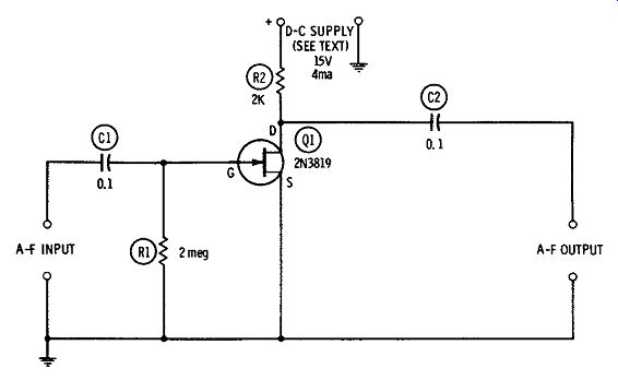
Fig. 1. Simple small-signal a-f preamplifier.
A-F OUTPUT
At a d-c supply voltage level of 6 volts ( 2.5 ma), the single stage gives a no-load voltage gain of 2.5. At 9 vdc ( 3.1 ma), the gain is 3.7. And at 15 vdc ( 4.0 ma), the gain is 8. The maximum signal input before output-peak clipping is approximately 0.58 volt rms.
Frequency response, referred to 1 kHz, is flat within 2 db from 50 Hz to 50 kHz. All gain figures are given on the basis of a ! megohm output load.
The 2N3819 is encapsulated in plastic and gives no installation problems. All wiring must be kept as short and direct as practicable, for reduction of stray pickup at the low signal levels at which this amplifier can operate.
The 2-megohm gate resistor ( R1) and 2000-ohm drain resistor ( R2) both are 1/2 watt.
SINGLE-STAGE, LOW-GAIN A-F PREAMPLIFIER
Higher gain than that afforded by the preceding circuit and higher output voltage, as well, may be obtained by self-biasing the FET. A low-gain circuit of this latter type, based on a 2N4868 FET, is shown in Fig. 2. Here, source resistor R3 (bypassed by capacitor C3) provides the required gate bias. Note the similarity of this circuit to that of the familiar grounded-cathode tube amplifier or the common-emitter bipolar-transistor amplifier. All resistors arc 1/2 watt, and electrolytic capacitor C3 is rated at 25 dcwv.
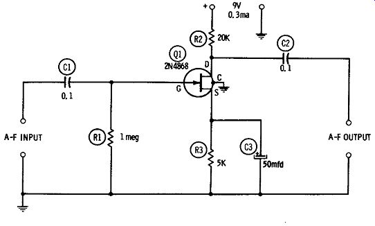
Fig. 2. Single-stage, low-gain a-f preamplifier.
With a d-c supply of 9 volts ( 0.3 ma), the open-circuit voltage gain is 20. The maximum signal input before output-peak clipping is 50 millivolts rms, and the corresponding output signal is 1 volt rms.
All wiring must be kept as short and direct as practicable to minimize stray pickup at the low signal levels at which this amplifier can operate. One pigtail of the 2N4868 is connected to the metal case of this FET and should be grounded, for shielding.
SINGLE-STAGE, MEDIUM-GAIN A-F PREAMPLIFIER
Higher voltage gain than that afforded by the preceding low-gain circuit is obtained with the self-biased, common-source a-f pre amplifier, based on a 2N4338 FET, shown in Fig. 3. Note here also the similarity of this circuit to that of a grounded-cathode tube amplifier or a common-emitter bipolar-transistor amplifier.
With a d-c supply of 15 volts ( 8 µ,a), the voltage gain ( open circuit) is 45, and the maximum signal input before output-peak clipping is 78 millivolts rms. This results in a maximum signal output of 3.51 volts rms. Frequency response, referred to 1 kHz, is flat within 0.5 db from 50 Hz to 20 kHz, and within 4 db from 50 Hz to 50 kHz.
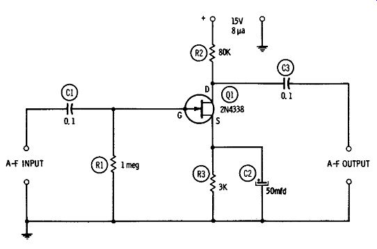
Fig. 3. Single-stage, medium-gain a-f preamplifier.
The 1-megohm gate resistor ( R1), 80,000-ohm drain resistor ( R2), and 3000-ohm source resistor ( R3) are 1/2 watt. Electrolytic capacitor C2 is rated at 25 dcwv.
All wiring must be kept as short and direct as practicable, · to minimize stray pickup at the low signal levels at which this amplifier can operate. Care must be taken also in the location of the 2N4338, since the gate electrode is internally connected to the metal case of this FET.

Fig. 4. A-f source follower.
A-F SOURCE FOLLOWER
Fig. 4 shows the circuit of a source follower employing a 2N4340 FET. Note that with its unbypassed source resistor ( R2) across which the output signal voltage is developed, this circuit closely resembles its counterparts-the tube-type cathode follower and bipolar-transistor emitter follower. Like the latter two circuits, the source follower is invaluable for transforming a high-impedance input to a low-impedance output. This circuit finds regular use, therefore, in matching a high-impedance output to a low-impedance transmission line, matching a high-impedance transducer to a low input-impedance transistor stage, etc. Fixed bias is provided by the 1.5-volt cell, M1. The voltage gain and maximum permissible input signal voltage are somewhat less when this cell is omitted.
With the d-c supply of 15 volts ( 1 ma), the voltage gain is 0.5, and the maximum signal input before output-peak clipping is 1.5 volts rms. This results in a maximum signal output of 0.75 volt rms.
Frequency response, referred to 1 kHz, is Hat within 1 db from 50 Hz to 100 kHz. The gain and frequency response are given here on a no-load basis.
The output impedance of the source follower is somewhat lower than the 1000 ohms of source resistor R2. In this instance, it is 700 ohms. This situation is similar to that which characterizes the cathode follower and emitter follower. In the FET circuit, where, Ro is the output impedance (resistance), in ohms, R. is the source resistance ( R2 in Fig. 4), in ohms, gm is the forward transconductance of the FET, in mhos, g0 is the output conductance, in mhos.
All resistors are 1/2 watt, and R1 may be raised as high as 22 megohms if a higher input impedance is desired. Input-circuit wiring must be kept as short and direct as practicable to prevent stray pickup by this high-impedance circuit. Care must be taken also in locating and mounting the 2N4340, since the metal case of this FET is internally connected to the gate electrode.
TWO-STAGE, R-C-COUPLED A-F AMPLIFIER
One of the advantages afforded by the high input impedance of the FET is the latter's adaptability to conventional r-c-coupled multistage amplifiers. As in tube practice, there is no limiting loss of gain between stages as there is in r-c-coupled bipolar-transistor amplifiers. Fig.2-5 shows the circuit of a 2-stage, r-c-coupled amplifier, employing two 2N4338 FETs (Q1, Q2). Cascaded, self-biased common-source stages are used.
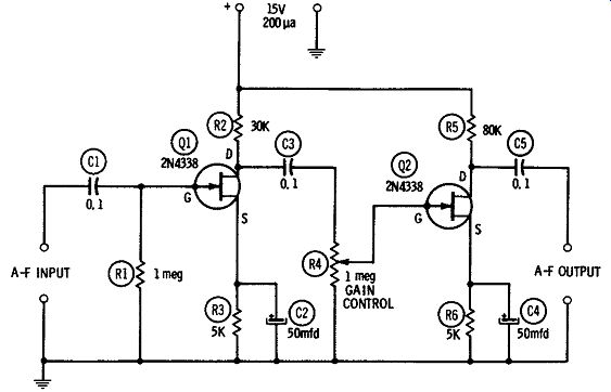
Fig. 5. Two-stage, r-c-coupled a-f amplifier.
The total d-c drain is 200 µa at 15 volts. With this d-c supply, the overall voltage gain of the amplifier is 1000 when potentiometer R4 is set for full output. At this level, the maximum signal input before output-peak clipping is 4 millivolts rms, and this corresponds to a maximum signal output of 4 volts rms. Frequency response, referred to 1 kHz, is down 4 db at 50 Hz and at 50 kHz. Gain and frequency-response figures are given in terms of a 1-megohm load across the output.
All resistors are 1/2 watt. Electrolytic capacitors C2 and C4 are rated at 25 dcwv. All wiring must be kept as short and direct as practicable, to minimize stray pickup at low signal levels. Care must be taken also in the location of the 2N4338's, since the gate electrode is internally connected to the metal case of this FET.
TWO-STAGE, TRANSFORMER-COUPLED A-F AMPLIFIER
The high input impedance of the FET makes practicable the use of step-up coupling transformers between amplifier stages, as is common in tube-type amplifiers. The additional voltage gain due to the step-up turns ratio of the transformer thus is easily obtained.
( In transformer-coupled bipolar-transistor amplifiers, on the other hand, the low input impedance of the bipolar unit necessitates a step-down ratio.)
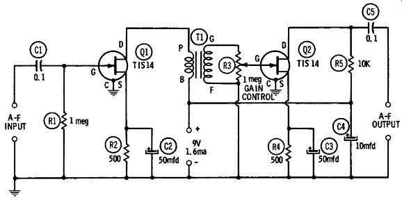
Fig. 6. Two-stage, transformer-coupled a-f amplifier.
Fig. 6 shows the circuit of a 2-stage amplifier employing trans former interstage coupling. Here, transformer T1 provides a 2:1 step-up, and may be any convenient tube-type interstage trans former. Note the usual primary ( P, B) and secondary ( G, F) labels.
This amplifier is based on two TIS14 FETs ( Q1, Q2); however, the same scheme may be used with other field-effect transistors.
In fact, some designers will favor transformer coupling to overcome the low voltage amplification provided by low-transconductance FETs.
At 1000 Hz, the voltage gain ( with potentiometer R3 set for full output, and the amplifier loaded with 1 megohm) is 3000. This corresponds to a maximum signal input of 1 millivolt rms for 3 volts rms output before output-peak clipping. For high gain, a higher turns ratio than the 2: 1 value of the author's transformer may be used. Frequency response of the amplifier is dictated largely by that of the transformer. Total current drain of the circuit is 1.6 ma at 9 vdc.
All leads must be kept as short and direct as practicable, to minimize stray pickup and stray coupling, and the transformer case should be grounded. A fourth pigtail of the TIS14 is connected to the metal shell of this FET and should be grounded, for shielding.
All fixed resistors are 1/2 watt, and electrolytic capacitors C2, C3, and C4 are rated at 25 dcwv.
IDGH-IMPEDANCE INPUT FOR BIPOLAR TRANSISTOR
A convenient application of the FET is the provision of high input impedance for a high-gain bipolar-transistor amplifier. In this instance, the FET serves as an input-impedance transformer.
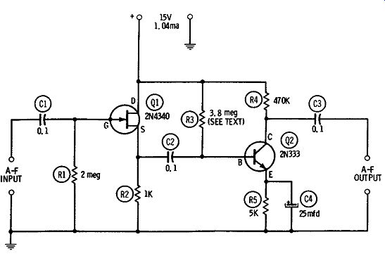
Fig. 7. FET high-impedance input for bipolar transistor.
Fig. 7 shows such an arrangement. Here, a 2N4340 FET source follower, similar to the one described earlier in this section, is connected ahead of a high-gain stage employing a 2N333 silicon transistor ( Q2). The 2N333 stage alone provides a voltage gain of 200 when bias resistor R3 is adjusted to an optimum value for the particular transistor used. And since the 2N4340 stage gives a voltage gain of 0.5, the overall gain of the complete circuit is 100 when the output is terminated with 1 megohm.
The maximum signal input before output-peak clipping is 20 milli volts rms, and this corresponds to a signal output of 2 volts rms.
The circuit draws approximately 1.04 ma at 15 vdc.
All resistors are 1/2 watt. Electrolytic capacitor C4 is rated at 25 dcwv. Either R1 or R2 may be made a potentiometer for gain control, although varying R2 will introduce less noise.
CONVENTIONAL PHASE INVERTER
Fig. 8 shows the circuit of a conventional two-triode a-f phase inverter based on two 2N4338 FETs ( Q1, Q2). The two outputs are 180 degrees out of phase with each other. Output 1 is 180 degrees out of phase with the input signal; Output 2 is in phase with the input signal.
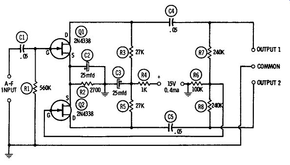
Fig. 8. Conventional phase inverter.
The circuit operates in the same manner as the equivalent tube type circuit. That is, the signal is amplified and inverted by transistor Q1, and the output of Q1 ( developed across resistors R7 and R6) is delivered to the OUTPUT 1 terminal. A portion of this output signal is applied to the gate of transistor Q2, and is amplified and inverted by this latter transistor. The output of Q2 ( developed across resistors RS and R6) is delivered to the OUTPUT 2 terminal.
Resistors R7 and RS may serve directly as the gate-to-ground resistors of a succeeding push-pull FET stage, or as the grid resistors if the push-pull stage contains tubes.
Like the equivalent tube circuit, this phase inverter is self balancing: The signal voltage developed across resistor R6 by the output of transistor Q2 bucks the signal voltage developed across this resistor by the output of Q1 ( these two voltages being out of phase with each other), and this action reduces the gate-to-ground signal voltage of transistor Q2 and thus keeps the signal at OUTPUT 1 and OUTPUT 2 substantially equal. The inverter draws 0.4 ma at 15 vdc.
Capacitor C3 and resistor R4 form a decoupling filter which promotes stability; these may be omitted in some layouts if there is no trouble from motorboating. All resistors are 1/2 watt, and electrolytic capacitors C2 and C3 are rated at 25 dcwv. In the 2N4338, the gate electrode is internally connected to the metal case of this FET; hence, care must be taken in the placement of this transistor.
PARAPHASE PHASE INVERTER
A single-FET ("paraphase") phase inverter, equivalent to the single-tube circuit, is shown in Fig. 9. This circuit, which employs a Ul83 FET, exploits the 180-degree phase difference between source output and drain output ( equivalent to cathode output and plate output, respectively), and provides the simplest arrangement for converting from single end to push-pull without a transformer.
The signal at the OUTPUT 1 terminal is 180 degrees out of phase with the input signal, that at OUTPUT 2 is in phase with the input.
And the equality of drain resistor R2 and source resistor R3, together with the large amount of degeneration supplied by the un bypassed source resistor, keeps these two outputs approximately equal. ( They may be equalized exactly through close adjustment of either R2 or R3, one with respect to the other.) The circuit draws 0.25 ma at 15 vdc.
The maximum signal input before output-peak clipping is 1 volt rms, and the voltage gain in each half of the circuit is approximately 0.8. Frequency response, referred to 1 kHz, is flat within 3 db from 50 Hz to 50 kHz. Gain and frequency-response figures are given for 1-megohm output load.
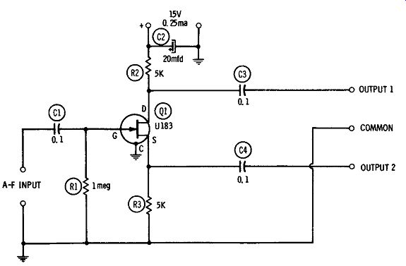
Fig. 9. Paraphase phase inverter.
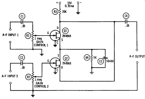
Fig. 10. Dual-channel audio mixer.
All resistors are 1/2 watt, and electrolytic capacitor C2 is rated at 25 dcwv. A fourth terminal of the Ul83 is internally connected to the metal case of this FET and should be grounded, for shielding.
DUAL-CHANNEL AUDIO MIXER
Fig. 10 shows a conventional circuit for mixing two a-f signals or for selecting one or the other. Like the equivalent tube or bipolar-transistor circuit, it provides separate inputs and a common output. Separate gain controls ( !-megohm potentiometers R1 and R2) are provided, and the resistances of these controls may be increased to 5 megohms each, if a higher input impedance is desired.
Using two 2N4868 FET's (Q1, Q2), the circuit gives maximum voltage gain of 10 per half. This corresponds to a maximum signal input of 15 millivolts rms for an output of 1.5 volts rms before output-peak clipping. Current drain is 350 µ,a at 15 vdc.
All resistors are 1/2 watt, and electrolytic capacitor C3 is rated at 25 dcwv. A fourth terminal of the 2N4868 is internally connected to the metal case of this FET and should be grounded, for shielding.
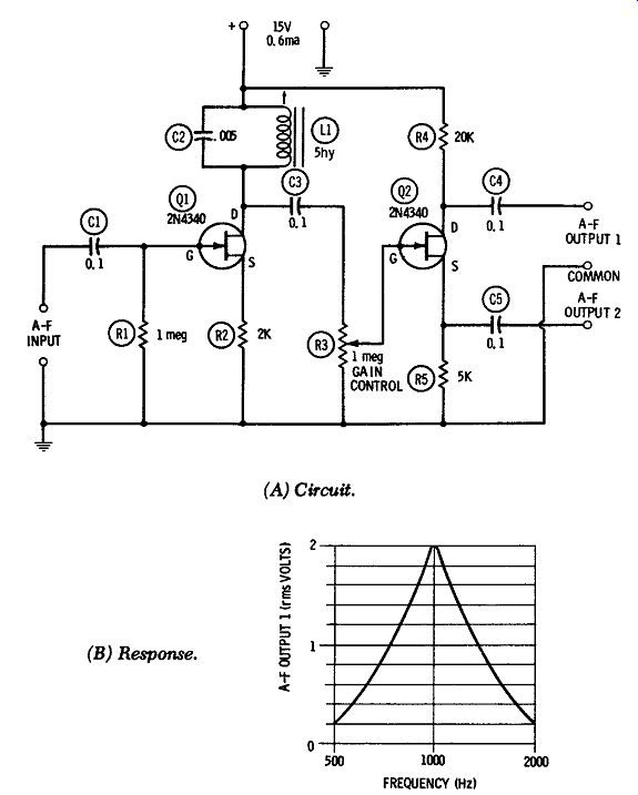
Fig. 11. L-c-tuned bandpass a-f amplifier. (A) Circuit. (B) Response.
L-C-TUNED BANDPASS A-F AMPLIFIER
An amplifier which can be tuned for peak output at a desired audio frequency is invaluable in bridge balancing, signal selection, telemetering, c-w signal peaking, selective signaling, and electronic control. Fig. 11A shows such a circuit which employs two 2N4340 FET's ( Q1, Q2) and is tuned by means of inductance and capacitance. Fig. llB shows the frequency response.
The first stage is a common-source amplifier with an unbypassed source resistor ( R2). The latter supplies substantial degeneration for stability and low distortion. The second stage is also a common source amplifier, with separate outputs from its drain ( high impedance) and source ( low impedance) to accommodate various loads.
With potentiometer R3 set for maximum gain, the maximum input signal before output-peak clipping is 7 millivolts rms. The corresponding maximum signal outputs are: A-F OUTPUT 1, 2 volts rms; A-F OUTPUT 2, 0.45 volt rms. The curve in Fig. llB is based upon a 1-megohm load for A-F OUTPUT 1. The circuit draws 0.6 ma at 15 vdc.
The inductance and capacitance values shown in Fig. 11A are given for 1-kHz operation: L1 is a U.T.C. Type VI-Cl5, 5.4-henry adjustable inductor ( or equivalent), and C2 is a .005-mfd mica capacitor. A tuning screw allows the inductance to be varied over a narrow range to set the frequency exactly to 1 kHz. Other operating frequencies may be obtained by changing the value of the coil inductance ( L1) or the capacitance (C2). If necessary, both inductance and capacitance can be varied.
All wiring must be kept as short and direct as practicable, to minimize stray coupling and pickup. The metal case of the 2N4340 is internally connected to the gate electrode, so this FET must be mounted clear of contact with other components. All fixed resistors are 1/2 watt.
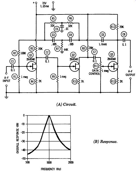
Fig. 12. R-c-tuned bandpass a-f amplifier. (A) Circuit. (B) Response.
R-C-TUNED BANDPASS A-F AMPLIFIER
Resistance-capacitance tuning of a bandpass a-f amplifier is a more compact arrangement than the inductance-capacitance tuning described in the preceding section. Fig. I2A shows a 1-kHz amplifier which is r-c tuned. Fig. 12B shows the frequency response.
The basic amplifier is a 3-stage unit, based on 2N4340 FETs ( Q1, Q2, Q3). Unbypassed source resistors ( R4, R10, and R13) supply a large amount of current degeneration for stability and low distortion. The overall voltage gain ( with 1-megohm output loading) is 42 db, with potentiometer R1l set for full output, and the odd number of stages rotates the phase correctly for negative feedback in the path through capacitor C6 back to the input.
Tuning is accomplished with a parallel-T network (C3, C4, C5, R5, R6, R7). This is a null network ( r-c notch filter) connected in the feedback loop between output transistor Q3 and input transistor Q1. The 1-mfd capacitor, C6, provides d-c blocking for this network, and 100,000-ohm resistor R2 limits the loading of the network. Negative feedback through the loop is sufficient, at the 42-db gain of the amplifier, to cancel the amplifier gain. However, the parallel-T network removes feedback voltage at the network null frequency. The result is transmission by the amplifier very sharply at that frequency, as shown by Fig. 12B. The values given for capacitors C3, C4, and C5 and for resistors R5, R6, and R7 are for 1-kHz tuning. Parallel-T networks may be set up for other desired frequencies, provided that the following relationships are maintained:
C C C,, 3 = 4 =2 Rs= Rs= 2R,
The pass frequency of the amplifier then is 1 f = 2 pi CR where, f is the pass frequency of the amplifier, in hertz, C is the capacitance of C3, in farads, R is the resistance of R5, in ohms.
The amplifier draws 1.65 ma at 15 vdc. All fixed resistors are 1/2 watt. The capacitors and resistors in the parallel-T network must be rated at 1 percent accuracy.
All wiring must be kept as short, rigid, and direct as practicable, for stable operation and minimum pickup of stray signals. The gate electrode of the 2N4340 is internally connected to the metal case of this FET, so the latter should be mounted out of contact with other components.
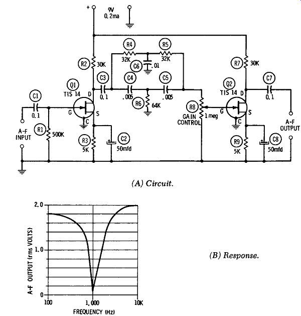
Fig. 13. R-e-tuned hand-suppression (notch) amplifier. (A) Circuit. (B)
Response.
R-C-TUNED BAND-SUPPRESSION (NOTCH) A-F AMPLIFIER
An amplifier which can be tuned sharply to eliminate an audio frequency is invaluable for suppressing a heterodyne in radiophone reception, eliminating an undesired c-w signal, separating one frequency from a mixture, and removing a single hum or noise component from a signal complex. Fig. 13A shows the circuit of a resistance-capacitance-tuned amplifier of this type, based on two TIS14 FETs ( Q1, Q2). Fig. 13B shows the typical frequency response that can be expected of the circuit. Note how a sharp drop in output of one band of frequencies can be designed into the circuit.
The tuning network is a parallel-T filter ( C4, C5, C6, R4, R5, R6) connected between the amplifier stages. The values given for the filter capacitances and resistances in Fig. 13A are for I-kHz elimination. Similar filters may be set up for other frequencies, provided that the following relationships are maintained: The null frequency then is 1 f = 2-n-CR where, f is the null frequency, in hertz, C is the capacitance of C4, in farads, R is the resistance of R4, in ohms.
If the filter capacitors and resistors are closely selected and the capacitors are high Q, the notch point ( see Fig. 13B) will be very close to zero. At some distance on each side of the notch frequency ( say at 0.1f and 10f), the a-f output will be 2 volts rms for a maximum a-f input of 3.75 millivolts rms before output-peak clipping. This assumes that potentiometer RS is set for maximum gain and that the amplifier is terminated with a 1-megohm resistive load.
All wiring must be kept as short, rigid, and direct as practicable, to promote stability and to minimize stray pickup and stray coupling. A fourth pigtail of the TIS14 is connected to the metal case of this FET and should be grounded, for shielding. All fixed resistors are 1/2 watt, and electrolytic capacitors C2 and CS are rated at 25 dcwv.
The amplifier draws 0.2 ma at 9 volts dc.
VIDEO AMPLIFIER
Fig. 14 shows the circuit of a simple video amplifier using a single 2N3819 FET. This circuit provides a voltage gain of 5: The maximum signal input before output-peak clipping, at I-megohm load, is 0.6 volt rms for 3 volts rms output. Stages may be cascaded for increased gain.
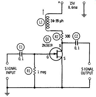
Fig. 14. Video amplifier.
The frequency response is within +2 db from 50 Hz to 4 MHz.
Inductor L1 ( Miller No. 4508, or equivalent) is adjustable by means of a screw-tuned slug from 24 to 35 µ,h and is set experimentally for flat output throughout the 50-Hz to 4-MHz range with a constant-amplitude signal applied to the SIGNAL INPUT terminals. Total current drain is 8.6 ma at 15 vdc.
Short, rigid leads are important in this circuit, to minimize strays and to stabilize operation. Resistors R1 and R2 are 1/2 watt.
455-kHz I-F AMPLIFIER
Because of the reverse transfer capacitance of the FET ( equivalent to grid-plate capacitance in a tube), the field-effect transistor will oscillate in an amplifier in which l-c tanks in the input (gate)
and output (drain) circuits are tuned to the same frequency, unless the circuit is carefully neutralized. Such a circuit is the conventional, transformer-coupled intermediate-frequency amplifier. Neutralization can be a nuisance, since special tapped i-f transformers for single-ended neutralization are not readily available except in the step-down type required by the bipolar transistor.
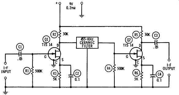
Fig. 15. 455-kHz i-f amplifier.
The i-f amplifier shown in Fig. 15 avoids this difficulty by using a 455-kHz ceramic filter (U.S. Sonics Type A25H4C, or equivalent) instead of a transformer. This filter, being self-resonant, requires no tuning, and is connected simply between two amplifier stages in place of the usual coupling capacitor. Its voltage insertion loss is approximately 1 db.
The amplifier employs two TIS14 FET's ( Q1, Q2) and provides an overall open-circuit gain of 400: The maximum i-f input is 2.5 millivolts rms before peak clipping occurs in the 1-volt rms output.
Selectivity of the circuit corresponds very closely to that of the filter alone, i.e., - 3 db at 2-kHz bandwidth to - 40 db at 160-kHz bandwidth. Total current drain is 0.2 ma at 9 vdc.
All wiring must be kept as short, rigid, and direct as practicable, to minimize i-f losses and to promote stable operation. A fourth pigtail of the TIS14 is connected to the metal case of this FET and should be grounded, for shielding.
AUXILIARY HEADPHONE AMPLIFIER
Often magnetic headphones must be connected to a receiver or other instrument without appreciably loading the device. This requires an auxiliary amplifier with high input impedance.
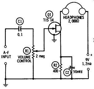
Fig. 16. Auxiliary headphone amplifier.
Fig. 16 shows the circuit of an amplifier with 2 megohms input resistance, driving a pair of magnetic headphones having 2000 ohms d-c resistance. This amplifier, based on a single TIS14 FET, provides a voltage gain of 40: This corresponds to a maximum a-f signal input of 75 millivolts rms before peak clipping in the 3-volt rms output signal ( potentiometer R1 is set for maximum volume). The circuit draws 1.2 ma at 9 vdc. This power may be supplied by a self-contained battery or may be taken from the power supply of the device which delivers the signal to the headphone amplifier.
Resistor R2 is 1/2 watt, and electrolytic capacitor C2 is rated at 25dcwv.
SIMPLE AUDIO AGC AMPLIFIER
The gain of the FET amplifier stage is easily controlled by varying the d-c gate bias voltage, the gain varying inversely with the voltage. When the control voltage is derived from some key signal point, such as the output of a multistage amplifier ( through rectification and filtering) and applied to one or more stages, automatic gain control results.
Fig. 17 shows a simple, one-stage a-f amplifier employing this principle. The d-c control voltage is applied at the CONTROL VOLTAGE INPUT terminals and acts as additional gate bias for the 2N4868 FET ( Q1). Initial operating bias is supplied by the voltage drop across source-bias resistor R4. The maximum current drawn from the control-voltage source is 60 microamperes.
When the d-c control voltage is zero, the voltage gain of the stage is 10, with a maximum undistorted output signal of 1 volt rms. When the control voltage is 6 volts de, the stage output is reduced to 0.5 millivolt rms ( better than 90 db range). A lower d-c control voltage may be used if less db change is needed. For minimum distortion, the maximum a-f input signal reaching the gate of the 2N4868 must be held to 0.1 volt rms. Total current drain is 0.5 ma at 9 vdc.
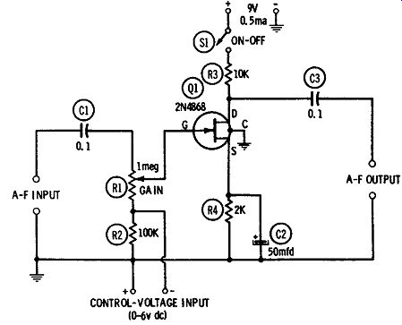
Fig. 17. Simple audio age amplifier.
All fixed resistors are 1/2 watt. The 50-mfd source bypass capacitor, C2, is a 25-dcwv electrolytic, and the 0.1-mfd input and output coupling capacitors, C1 and C3, are 100-volt plastic or paper units.
A fourth pigtail of the 2N4868 is connected to the metal case of this FET and should be grounded as shown, for shielding.
The circuit has a great many uses other than conventional automatic gain control in an audio amplifier. Any application is feasible in which an adjustable or fluctuating d-c voltage ( at virtually zero power) is available for varying the output of an audio channel.
When the control voltage is positive with respect to ground, use a P-channel FET (such as a 2N3578), changing the values of R3 and R4 as required and reversing capacitor C2.
SIMPLE D-C AMPLIFIER
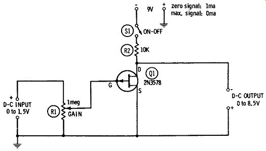
Fig. 18. Simple d-c amplifier.
Fig. 18 shows the circuit of a simple one-stage d-c voltage amplifier, employing a 2N3578 FET ( Q1). This stage has a no-load voltage gain of 5.65. Similar stages may be cascaded for higher gain, provided proper arrangements are made for biasing the gate source junction of each stage.
When the d-c input signal is zero at the gate of the 2N3578, there is a maximum drain current of almost 1 ma through drain resistor R2. This produces a voltage drop across R2, which reduces the d-c output voltage to approximately 0.35 volt ( "false zero"). If exactly zero output is desired, the residual voltage may be eliminated with a common output-bucking circuit. When the d-c input signal is 1.5 volts at the 2N3578 gate, the drain current is cut off, and the output rises to - 8.5 volts. The output values given above are for zero loading. This condition obtains only when the amplifier feeds a high resistance device, such as an oscilloscope, vtvm, or other amplifier.
(At 10,000-ohms load, the output drops to 5 volts dc). Because a positive input signal gives a negative output signal, the amplifier is an inverter as well, and this feature will be welcome in a number of applications. The unit is also a kind of current amplifier: virtually all of the signal-input current is accounted for in gain control potentiometer R1, ( 1.5 µ,a at 1.5 volts input), whereas the output current flows through an external load as the result of the amplified d-c voltage. This is 500 µa in a 10,000-ohm load-a current gain of 332. ( The current and voltage gains referred to here indicate a d-c power gain of 1,000,000 plus). A simple d-c amplifier of this type is useful in control systems as well as in instruments. For example, it will drive a 10,000-ohm. 5-volt d-c relay, with an input signal of only 1.5 volts at 1.5 micro amperes. Various thresholds of operation may be obtained simply by adjustment of gain control R1.
Layout of the amplifier is not critical. However, the 2N3578 must be mounted clear of wiring and other components, as the gate lead is internally connected to the metal case of this FET. Drain resistor R2 is 1/2 watt.
[Note: This guide is based on Sams "FET Circuits", pub'd in 1961]