A variable law, low distortion attenuator incorporating second harmonic cancellation circuitry
Compression and limiting play an increasingly important role in the resources of a modern sound/studio. The conventional function of signal level control is to avoid overload, but it can be used in the realm of special effects. To date, however, relatively few designs for high-fidelity compressor/limiters have been published.
The main design problem is the voltage-controlled attenuator, v.c.a., which increases attenuation of the input signal in response to a voltage from a control loop as shown in Fig. 1. In limiting, this circuit block continuously monitors the peak output level from the v.c.a. and acts to maintain an almost constant level if it exceeds a threshold value, or, in compression, allows it to increase more slowly than the v.c.a. input signal, This is illustrated in Fig. 2., which shows the input-amplitude/output-amplitude characteristic for both compression and limiting. Note that limiting makes use of a much tighter slope to ensure that the output voltage cannot exceed the chosen limit, and that the threshold (point of onset of attenuation) takes place at a higher level than for compression.
Traditionally, studio-quality compressor/limiters (as the two functions are so similar it is logical to produce a system that can be used for either compression or limiting) used, one of two types of v.c.a. Either the audio signal was chopped at an ultrasonic frequency by a variable mark/space square wave which requires complex circuitry and careful filtering of the audio output to avoid beats with tape-recorder bias frequencies --or it was attenuated by an electronic potential divider, one. arm of which was a photoresistor, the control signal being applied via a small filament bulb. The last-mentioned has disadvantages because photoresistors are non-linear devices, therefore noticeable distortion is introduced into the audio signal, and the thermal inertia of the bulb filament limits the speed of attenuation onset.
Most modern compression systems use field-effect transistor operated below pinch-off as a voltage-variable resistance in a potential divider. This technique has many advantages; it is a simple; cheap, and fast-acting configuration that can provide an attenuation variable between 0 and 45dB. The only problem is that an FET is a square-law device, and tends to generate a level of second-harmonic distortion that increases rapidly with signal amplitude.
A typical arrangement is shown in Fig. 3.
R2, R3 and C2 allow the source of the f.e,.t. to be set at a DC level above ground, so that a control-voltage that moves positive with respect to ground can be used, to avoid level-shifting problems in the control loop. This DC level is isolated from the input and output by c,. The distortion introduced by this circuit is at its worst for the 6dB attenuation condition, because at this point the drain-source resistance equals R(, and the maximum power level exists in the FET Table 1 shows the level of second-harmonic distortion introduced into a sine-wave signal of 100 mV RMS amplitude, under the 6dB attenuation condition, for three different FET types.
Measurements were made with a Marconi TF2330 wave analyzer, higher orders of harmonic distortion proved to be negligible amplitude in all cases.
These measurements were made on one sample of each type of FET and, because production spreads are large, the results should be treated with some caution. However, it is clear that these levels of distortion are unacceptable for high-quality applications.
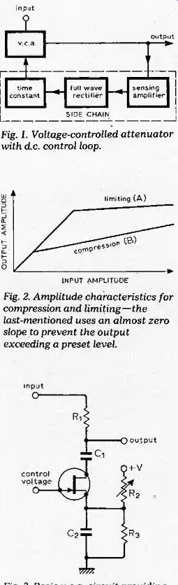
Fig. 1. Voltage-controlled attenuator with DC control loop.
Fig. 2. Amplitude characteristics for compression and limiting-the last-mentioned uses an almost zero slope to prevent the output exceeding a preset level.
Fig. 3. Basic v.c.a. circuit providing up to45dB of attenuation. This configuration introduces second-harmonic distortion which is greatest at 6dB o/ attenuation.
Fortunately, a technique* exists for reducing FET distortion to manageable levels, if the control-voltage is applied to the FET gate and summed with a signal consisting of one-half the voltage from drain to source, then the distortion level is dramatically lowered. The configuration in Fig. 4 shows a simple way of realising this; the signal fraction fed back is not critical and 10% resistors can be used for R4 and Rs. Surprisingly, this distortion cancellation procedure leaves the attenuation/control-voltage characteristic almost unchanged. Table 1 shows the new maximum distortion values for 100mV RMS input. (Note that the maximum no longer occurs at 6dB attenuation. but at a point that varies with the FET type, where cancellation is least effective.) From these results the. 2N5457 and 2N5459 are superior, the 2N5459 was used in the final version of the v.c.a.
To determine appropriate signal levels in the v.c.a., measurements were made of maximum distortion generated, ie the v.c.a. was set to 2dB attenuation, against RMS input voltage; results are shown in Table 2. The. question now arises as to whether this distortion performance, is adequate for a high-quality compressor/limiter. There is no general agreement as to the amount of second harmonic distortion that can be introduced into a program signal before it becomes aurally detectable, but 0.1% is a figure that is quoted. This means that the permissible input voltage to the v.c.a, would be restricted to below 100 mV RMS In practice, however, the attenuation level will be constantly changing, and because distortion level peaks fairly sharply with attenuation change, this level of distortion will only be present for a very small percentage of the time. In any case, second harmonic distortion alone has a relatively low "objectionability factor". The proof of the pudding is in listening to the compressor output signal; inputs of music around 200mV RMS produced no trace of audible distortion. (Good class A power amplifiers and headphones were used for monitoring). The control loop consists of an amplifier which senses the v.c.a. output level. A full-wave rectification system is normal practice because program waveforms have positive and negative peaks that can vary by as much as 8dB, and an SdB uncertainty in the output, level is usually unacceptable. A time-constant arrangement is used with the rectification circuit to control the attack and decay rates.
The output sensing amplifier in the system is a non-inverting op-amp which allows a high input impedance because the output impedance of the v.c.a. stage reaches a maximum of about 39k ohm at zero attenuation. The full-wave rectification system consists of a transistor phase-splitter driving two op-amp precision-rectifier stages in antiphase. The principle of a precision rectifier is illustrated in Fig. 5. The rectifying element, is placed in the feedback loop of an op-amp, so that the effect of the forward voltage drop on the output voltage is divided by the open-loop gain. During positive half cycles, if the input voltage exceeds the DC level stored on the capacitor C, the op-amp output swings positive and C is charged through diode D until its stored voltage is equal to the input voltage. Thus C takes up a voltage across it equal to that, of the positive peak of the input signal. During negative half-cycles, and while the input is less than the voltage on C during positive half-cycles, the op-amp saturates negatively and D remains firmly reverse biased. Obviously this is only a half-wave rectification circuit, the full-wave version uses two of these driven in antiphase, and charging a common capacitor. A resistance through which the charging currents flow determines the attack time, and another in parallel with C defines the decay time constant.
The complete circuit is shown in Fig. 6. The v.c.a. is essentially as described above and the attenuation threshold is set by the variable resistance R2. As the resistance is increased the level of control voltage required for attenuation to begin is reduced, and the system's input/output characteristic moves smoothly from A to B on. Fig. 2. The threshold decreases and the compression slope becomes less flat as the. system turns, slowly from a limiter into a compressor by the manipulation of a single control. The output sensing amplifier consists of IC1 and has a gain of 19 over the audio band. This is rolled off to unity at DC by C5. Transistor Tr2 and its associated components form a conventional phase-splitter driving IC1 and IC3, the precision rectifiers. The rectifier circuitry is more complex than implied above, three modifications have been made improve the performance.
Firstly, IC2 and IC3 charge C9 via. current amplifier stages.
Tr5 and Tr6 otherwise the current-limited. 741 outputs would be unable to provide enough current for the faster attack times (less than 1mS). Secondly, the feedback loop from C9 to the inverting inputs of IC2 and IC3 is completed via a FET source-follower. Without this, Cy would be loaded by the two 741 inputs, and this would severely limit the maximum decay times available. Incorporating the source-follower allows decay times of several minutes by using large resistance values for R,7. The conventional source-follower has a large negative offset voltage and is unusable in this application because due to their rectifying action IC2 and IC3 are unable to provide a voltage on CB that is negative of ground. This would be required to allow the source-follower output to be at ground when there is no input to the rectifiers. However, if a modified source-follower is used, with a constant-current source and resistance, combination in the source circuit, the offset voltage can be varied on either side of zero by manipulation of which varies the driving current. The offset voltage is arranged to be plus 0.3V, to allow a large safety margin for thermal variations, component ageing, etc. This means that under no-signal conditions C9 takes up a standing quiescent voltage of plus 0.3V. The effect of this is taken up in the calibration of R2.
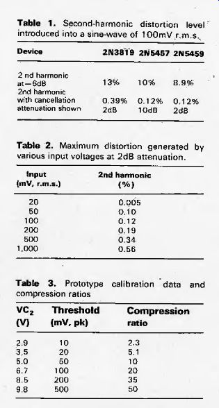
Table 1. Second-harmonic distortion level introduced into a sine-wave of
100mV RMS
Table 2. Maximum distortion generated by various input voltages at 2dB attenuation.
Table 3. Prototype calibration data and compression ratios
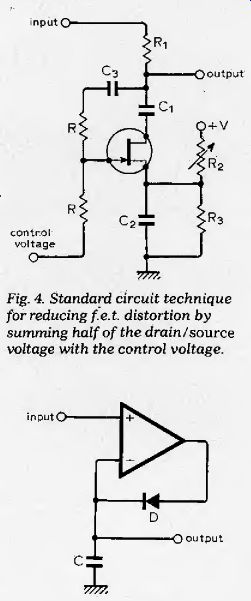
Fig. 4. Standard circuit technique for reducing FET distortion by summing
half of the drain/source voltage with the control voltage.
Fig. 5. Basic precision rectifier circuit where the rectifying element is in the feedback loop of an op-amp.
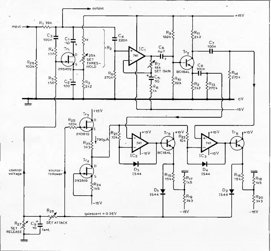
Fig. 6. Complete circuit where the output is taken directly from the v.c.a.
this may be buffered for loads greater than 100 kO.
The third modification is the addition of R21, D3, and R22, D4. These two. networks prevent IC2 and IC3 from saturating negatively, during negative half-cycles of their input voltage, by allowing local negative feedback through D3, and D4. This limits the negative excursion of the IC outputs to about two Volts. The prevention of saturation is necessary because the recovery time of the 741s causes the frequency response of the precision rectifier circuit to drop off at about 1kHz. The addition of the anti-saturation networks provides a frequency response that starts to fall off significantly above about 12khz. which is ample for our purposes as program signals have very little energy content above this frequency.
The final part of the circuit defines, the attenuation time constants. Resistor R26sets the attack time constant and R27 the decay time constant; these can range between zero and IMQr220/is and 10s) for R26, and IRQ and infinity (10mS and 20min) for R27. They can be either switched or variable resistances, depending on the range of variation required.
The circuit in Fig. 6 shows the compressor output being taken directly from the v.c.a. This is only suitable if the minimum load to the output is greater than 100 k-O, otherwise the v.c.a. attenuation characteristic will be distorted by excessive loading. If lower resistance loads are to be driven a buffer amplifier stage must be interposed. The IC, amplifier stage is suitable for most applications, and its gain is (R7+R8)/R8. For the unity gain case Rs & C5 can be eliminated and R7 replaced by a direct connexion.
The compressor should be driven from a reasonably low impedance output. (less than 5 kO). Construction is straightforward; the layout is not critical and the prototype was assembled on 0.1 in matrix Veroboard. To set up the circuit R24 is adjusted so that the voltage across C9 is about plus 0.3V with no signal input.
The value required will vary due to production spreads in the FETs. To calibrate R2 it is necessary to relate the level of input signal at which attenuation commences, with the voltage across C2. This can be done with an oscilloscope, or preferably an AF millivoltmeter. As a guide the calibration data for the prototype is shown in Table 3, along with the values of the compression ratio (number of dBs the input must increase by to increase the output by 1dB). This data must be regarded as only a guide. It is worth noting that as the controlling factor setting the compression/limiting function is the voltage across C2 R? could be replaced by a 1 k-O resistor connected to a remote voltage source.
The compressor/limiter is quite straightforward in use, provided a few points are kept in mind. Firstly, if it is being used in the limiting mode to prevent overload of a subsequent device, the fastest possible attack time should be used, to catch fast transients, and a fast decay time (say 100ms; R27= 10 k O), to allow the system to recover rapidly when the transient has passed. Secondly, if a noisy program signal is being compressed a long decay time should be employed, otherwise the noisy background will be faded up during quiet passages, and the familiar compressor "breathing noises" will be heard. Finally, signals with a large v.l.f. content should be avoided or filtered, otherwise v.l.f modulation of the signal will result, if a fast decay time is in use.
If a stereo compressor/limiter is constructed from two of the systems described above it is necessary to gang together R2, R26, and R27 between the two channels. A direct connexion between the non-grounded sides of the two C9’s is also needed. It might be necessary to select matched FETs to avoid stereo image shift during compression, due to differing attenuation characteristics in the two v.c.as. A well-smoothed p.s.u. providing + 15V should be used to power the compressor / limiter.
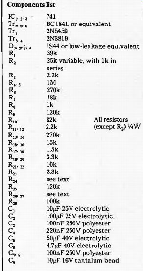
-- Components list
by D. R. G. Self, B.A. University of Sussex, UK.