This might show you a thing or two about how to recognize the good, the bad and the indifferent among soldered joints.
SOLDERING IS somewhat of an art and is essential to the successful construction of electronic circuits. The beginner particularly must learn to solder correctly to achieve success and avoid frustration.
Components are supported by a variety of methods and connections rely on the soldered joint. The solder is not meant to provide mechanical support.
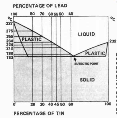
Fig. 1. How the melting temperature and plastic range are affected by
the relative percentages of lead and tin in a solder alloy. At the 'eutectic
point', an alloy of 63% tin and 37% lead goes from the liquid to the
solid state at 1 8 3°C without going through a plastic phase. This makes
it very brittle, and different contraction rates of the parts of the
joint cause the solder to fracture. A small plastic range, such as for
6 0/4 0 solder, prevents this.
Solder
Solder is an alloy of tin and lead that melts at fairly low temperatures. A joint is made using solder as a filler and bonding agent. Soldering creates a continuous intimate contact between the solder and the metal surfaces by the mechanical interlocking of the solder with the irregular surface texture of the metals. This process is called 'wetting', as the solder flows onto and into the metal surfaces. The wetting of the metal surface by the solder is important in making a joint electrically and mechanically sound.
All metals oxidize, or tarnish, on the surface as a result of being exposed to air. This prevents the solder from wetting the metal surface, resulting in a poor joint; 'flux' is used to remove tarnish. For electronic work this is composed of resin (sometimes spelt rosin), which is obtained from the sap of pine trees plus additives called 'activators'. At soldering temperatures, the activators decompose, liberating an acid that dissolves the tarnish faster than pure resin. Other fluxes are also made for non-electronic uses, usually sheet-metal work, copper and brassware manufacture. These fluxes are usually highly corrosive (such as hydrochloric acid) and must never be used for electronics work as even minute amounts rapidly corrode component leads and printed circuit board tracks.
Solder for electronics work is made as different gauge wires. Most have a resin core along their length, some have up to five separate cores.
The resin core melts before the solder and flows onto the joint, wetting both the joint and the solder, excluding the air. At the same time the activators dissolve the tarnish on the surface, allowing the solder to flow freely and properly wet the joint. When the solder melts, the increase in temperature deactivates the flux, limiting the possibility of corrosion. It is important to thoroughly heat activated resin during soldering to ensure the complete decomposition of the activators, otherwise they remain corrosive at normal temperatures.
Fig. 2. Construction of a 5-core multicore solder. The flux cores are
located near the surface so that they melt faster, giving rapid fluxing
action.
Resin-cored solder is obtainable in a variety of wire gauges. For general and heavy work, such as on sockets, chassis, switch contacts, etc, 16 gauge is suitable. For fine work on printed circuit boards, miniature components, etc, 20 or 22 gauge is best. It pays to have several different gauges handy. Experience will show which is the best under different circumstances.
As already mentioned, solder is an alloy of tin and lead. Tin melts at 327°C and is plastic down to 283°C. Lead melts at 232°C and is plastic from 183°C to 232°C. Either by itself is unsuitable as any movement of the joint while the soldering metal is in its plastic state will result in a faulty joint.
An alloy of appropriate proportions has a plastic state temperature range that is much smaller, and a lower melting point (see Fig. 11. With a composition of 63 % tin and 37 % lead, the alloy has no plastic region. It goes from solid to liquid at exactly 183°C. This is undesirable as a small region of plasticity reduces brittleness under practical circumstances. The most common composition of solder for electronics work is therefore 60% tin - 40% lead, often called 60/40 solder. It melts at a temperature of 188°C and has a plastic range of about 5°C. It combines optimum strength with lowest electrical resistance. Another type of solder used in electronics work includes about 1.5% copper and is known under the trade name of Savbit. Soldering irons with copper tips corrode rapidly when used with straight 60/40 solder as some of the copper is absorbed into the molten solder. Savbit solder prevents this and can extend the life of copper bit soldering irons by up to ten times.
Some soldering tools have iron-plated tips to reduce this sort of wear and the use of Savbit is not necessary with these irons.
Ordinary solders, such as 60/40 solder, are also referred to as 'soft solder'. Joints that have to withstand high temperatures, or that need greater mechanical strength than obtained with 60/40 solder, are joined with 'hard' solders that melt at higher temperatures. Hard solder contains either 30/70 or 20/80 tin-lead and melts at 255°C and 275°C respectively.
'Silver' solder, containing 5% tin/93.5% lead/1.5% silver, melts at about 300°C and is mostly used in fabricating brass or copper chassis, etc. Silver solder is usually melted with a gas-burning torch. A special flux is also used.
Low-temperature solder is also obtainable and is used where components may be damaged or where it is necessary to solder onto a joint that is already soldered without melting the existing joint. This has most applications in special servicing jobs. It consists of 50% tin/33 % lead/17 % cadmium and melts at 145°C. It requires care in soldering as it tends to fracture the instant it solidifies.
Soldering Irons
It is important to select a suitable soldering iron--after all, it will probably be the tool you use the most! A bewildering variety of types and sizes are available.
Continuous Heat Irons
These are probably the most widely used despite a few drawbacks. They are heated by a wire resistance element located in the barrel just behind the tip.The most suitable rating for electronics work is between 15 and 30 watts. Tools below this rating generally do not have sufficient heat capacity, while those above have high tip temperatures that can result in damaged components and poor joints. Irons of the continuous heat type that have ratings above 80 watts are best for sheet metal work. Irons advertised as 'universal' (mostly having a rating of 40 or 50 watts) should be avoided as they are usually too bulky for electronics work, particularly on printed circuit boards, and have too much heat capacity and high tip temperatures with the likelihood of component damage. The handle also usually gets too hot for comfort.
Choose an iron which is comfortable to hold. As well as being light, the iron should preferably have a lightweight power cord to reduce drag on your wrist when moving the iron around. The length of the cord should be adequate--about 1.5 m to 2 m is a good length.
Continuous heat irons are slow to heat to soldering temperatures--they are usually left running continuously. This causes tip oxidization which therefore requires constant maintenance and fairly frequent replacement. These are minor drawbacks, however, if you cannot afford a more expensive iron.
Some irons of this type are obtainable with a temperature select switch in the handle. This usually doubles the power when needed to provide sufficient heat to make the occasional heavy joint. They are normally used on the lower power position for routine soldering.
Quick Heat Irons
These irons operate from a low voltage at a high current, usually supplied from a transformer, and take only a few seconds to reach soldering temperature. They take only a few more seconds to reach red heat if the operating button is held on too long. Quick heat irons are made in two basic styles--the soldering gun and the low-voltage iron.
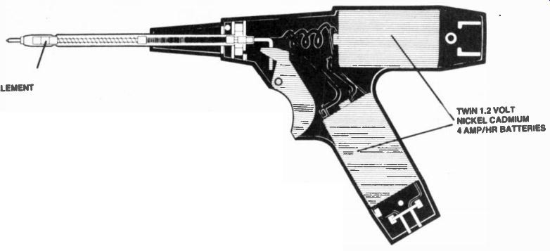
Fig. 3. A battery-operated soldering 'gun' (this one is by Scope, tool.
Construction is similar to the Mini Scope. Such irons are useful where
power is unavailable.
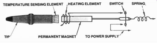
Fig. 4. Temperature control system that exploits the 'Curie point temperature'
of a magnet to turn the power on and off to the heating element. The
magnet is attracted to the rear of the tip, closing the switch. The element
heats the tip and when the temperature reaches the Curie point of the
magnet, the magnet loses its magnetism and the spring opens the switch.
When the temperature drops below the Curie point, the cycle is repeated.
Some models of the Weller soldering irons employ this technique of temperature
control.
Soldering guns have a transformer mounted in the handle that passes about 50 amps at 0.5 volts through a short length of heavy copper wire--the bit--thus heating it rapidly to high temperatures. Some irons of this type include a reel of solder which is automatically fed to the tip each time the trigger is pressed--but for good joints that's not where you want the solder; it needs to be applied to the joint.
Low-voltage irons have a push-ring or lever on the handle which pushes a carbon contact against the rear of the tip, passing a current of about 30 amps at 3 volts. The contact, having a higher resistance than the rest of the circuit, rapidly heats up, passing its heat to the tip, which reaches soldering temperature in a few seconds. An external transformer supply is the necessary power.
Quick heat irons are suitable for intermittent handyman use or applications requiring their large heating capacity. They are not recommended for general electronics use, particularly on printed circuit boards. They require some skill to control the heat so as not to damage components by overheating. Some do not have an electrostatic screen on the transformer, and ICs and some transistor (particularly MOSFETs) can be damaged by leakage currents.
Despite their limitations, quick heat irons can be useful in an electronics workshop. If you contemplate purchasing one make sure the transformer has an electrostatic screen.
Soldering guns have the disadvantage that the transformer in the handle tends to make them a little unwieldy, especially for prolonged use.
Battery-operated soldering irons have become widely available, and these find application where power is unavailable or inconvenient to supply.
These irons can be used where components sensitive to leakage currents (i.e. MOS devices, CMOS ICs, etc.) are employed. Rechargeable batteries, usually contained in the handle, supply the current. They are not suitable for prolonged use.
Temperature-Controlled Irons
Temperature-controlled irons are made specifically for electronics work. They are unsurpassed for good soldering, convenience and minimum possible damage to components. They are more expensive than the other types but get one if you can afford it.
There are several ways of controlling the tip temperature. One method (used in the Weller iron) is illustrated in Fig. 4. A spring-loaded switch within the handle is operated by a magnet and temperature-sensitive sensor assembly located in the barrel.
The temperature-sensing element consists of a ferro-magnetic material, which at a certain temperature (called the Curie point temperature), loses all magnetic properties. The actual Curie point temperature depends on the composition of the ferromagnetic material. The Curie point for iron is typically 1000°K, 633°K for nickel and 1393°K for cobalt. An alloy of these and other ferromagnetic materials can be selected to produce any temperature required.
When the tip is cold the magnet is attracted to the sensor, which actuates the switch, applies power to the element, and heats the tip. When the tip reaches the Curie point temperature the sensor releases the magnet, opening the switch and removing power from the heating element. When the tip cools slightly, the magnet is again attracted to the sensor and the whole cycle is repeated, maintaining the tip within a few degrees of the selected temperature. The iron can be heard to emit a small click as the magnet goes through its attract-release cycle.
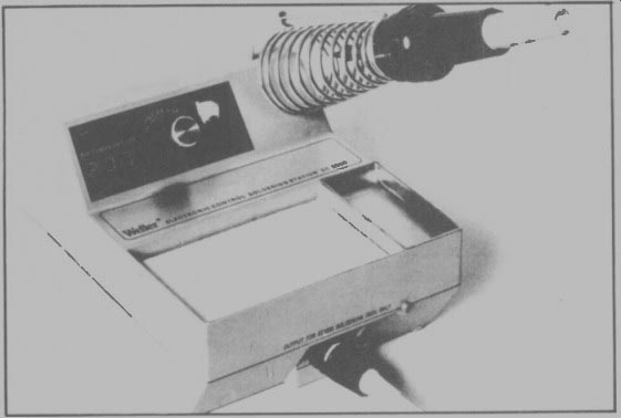
Fig. 5. This iron, Weller's model EC2000D, employs a temperature sensor
in the tip and electronic control of the power to the heating element
to maintain the tip temperature within very close limits. The desired
temperature is set by a knob and displayed in the three digit readout.
The tips are removable and sensors having different Curie point temperatures are available. One can select tip temperatures in the range 260°C to 430°C. A variety of shapes is also available to suit different applications. The Weller irons operate from a 24 volt transformer which is molded into the stand supplied.
Another type of controlled temperature iron has circuitry in the stand supplied with it which monitors the tip temperature and controls the supply to the heating element, thus maintaining a constant tip temperature.
In this type, a control knob is provided in the stand which allows the operator to set the desired tip temperature (Fig. 7). Where 60/40 solder is used for construction work, a tip temperature of 250°C (500°F) is recommended. This is sufficiently above the melting point of 215°C to allow for heat conducted away by the joint and still melt the solder. If using Savbit solder, it melts at a slightly higher temperature and a tip rated at 275°C (550 °F) is recommended.
For desoldering, such as in servicing work, a tip temperature of 315°C (600 °F) or more is necessary; up to 370°C 1700°F) is recommended where large connections are involved.
Soldering Bits
The soldering iron bit conducts heat from the iron's element to the joint. A typical bit is shown in Fig. 6.
The tip temperature and the amount of heat it stores are important factors in obtaining a good soldered joint. The tip temperature will drop when making a joint due to heat being conducted away by the parts of the joint. Just how much the temperature drops and how fast depends on the capacity of the bit to store heat and the mass of the parts being joined. The larger the bit, the more heat it will store and transfer to a joint, and the les will be the temperature drop. Temperature controlled irons minimize these problems to a large extent.
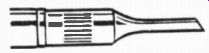
Fig. 6. A typical replaceable soldering iron bit. This one screws onto
the end of the iron barrel, and the cylindrical tip has a 'flat on the
end at an angle of about 60° to the axis.
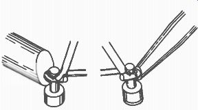
Fig. 7. The bit should be large enough for the job, otherwise too much
heat is conducted away from it by the joint and the solder will not flow
properly. The bit on the left is OK, that on the right is too small.
For an adequately rated iron, the correct bit for the job will remain above soldering temperature (without burning the joint) and cause the solder to flow properly. If the tip is too small, too much heat will be conducted away, and the solder, while it may melt a little initially, will not melt and flow properly and a poor joint results. The effect of proper bit size is shown in Fig. 7.
Bits are usually made of copper, copper alloy or iron-plated copper. A plated bit is shown in Fig. 8.
Unplated bits transfer heat more effectively but oxidize rapidly, reducing their efficiency. Their life is much shorter than plated bits and they require more frequent maintenance.
The area of the tip face determines the rate of heat transferred to the joint.
A small area will have a higher temperature but less heat reserve (or capacity) than a large tip. Generally, the more heat the work is likely to absorb, the larger the tip area should be. However, the area should not be so large that it obscures the work or damages adjacent parts.
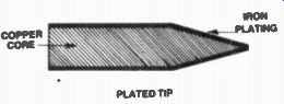
Fig. 8. Plated bits last longer because they do not oxidize as rapidly
as unplated bits.
They are usually iron-plated.
The distance the bit protrudes from the barrel of the iron is also important.
The shorter this distance, the higher the tip temperature. Usually, it is best to select a bit length as short as practicable to reduce the heat path from the element to the tip, and to minimize wobble and bending of the bit. It should not be so short that the barrel touches or radiates onto nearby components or that the tip temperature becomes too high. One way of reducing the temperature of a small diameter bit is to increase the length beyond that used for the larger-sized bit--or vice versa. Bent bits can be used in awkward places where a straight bit cannot reach.
Maintaining The Iron And Bit
'For maximum efficiency and consistently good joints, the soldering iron and bit require frequent but simple maintenance. Heating produces oxidization of the barrel and bit, the oxide forming a scale on the parts. This reduces heat transfer as the scale is an insulator. Continuous heat irons are particularly affected. Excessive scaling is produced by high operating temperatures and by prolonged use without descaling.
To remove scale, remove the bit and tap both the barrel and bit firmly on the bench top. This should be done regularly. Only remove a plated bit from the barrel of an iron when it is quite cold.
For efficient transfer of heat from the bit to the work, the face of the bit should be smooth and coated with a shiny layer of resin-free solder. A bit in this condition is said to be 'tinned'. A clean, new bit is tinned by heating it to soldering temperature (test it by lightly touching solder on the face of the bit) and applying a small amount of solder to the face and letting it flow freely to cover the face. Any excess should be removed by wiping it on a lightly damped sponge or cloth.
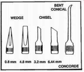
Fig. 9. Bits can be obtained in a variety of shapes to suit the job,
such as conical, wedge, bevel, chisel, etc. The most common bit shapes
are the wedge (or chisel) and the bevel. They can be different diameters
and lengths, giving different heat capacities.
With use, the face of the bit becomes pitted and the solder layer takes on a dull grey appearance. During soldering, some of the copper from the face is absorbed into the solder and with repeated use the surface becomes uneven. There is less absorption with plated tips. Copper bits in good condition and in bad condition are illustrated in Fig. 10. The 'pitting' can be removed by filing. Only file off as much as necessary to produce a smooth face again. Excessive filing reduces the heat capacity and increases the bit temperature. Remove any scaling as well. When a clean tip is obtained, re-tin the face. Do not pull the tip further out from the barrel to compensate for reduced length as this overheats that section of the heating element not in contact with the bit, producing excessive scaling and eventually causing the element to fail.
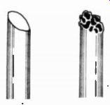
Fig. 10. The tip should be in good condition, as at left, for good soldering,
not worn, pitted or oxidized as at right.
Small surface irregularities on plated tips should be repaired with fine emery cloth when the tip is cold. Take care not to remove the plating. After cleaning, heat the bit and re-tin the face. Relatively large pitting on a plated bit means that some plating has come off. Attempts to remedy the situation usually result in more plating being removed. In such cases, replace the bit.
During normal soldering with a plated bit, the molten solder on the face should be replenished regularly while the tip is hot. The face can be cleaned by wiping it on a damp, fine textured sponge (these are usually supplied with controlled temperature irons). Do not overdo it or you will remove all the molten solder. Wait a few seconds after wiping the bit to allow it to recover heat and then lightly re-tin the face. Plated bits should have a small amount of excess solder on the face while not being used.
With either plated or unplated bits, regular cleaning during use is a good practice, making soldering easier and ensuring good joints. A damp sponge pad is good for either type of bit. A fine textured wire brush may also be useful with copper bits. (Fig. 11.)
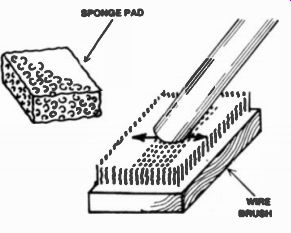
Fig. 11 The tip should be cleaned regularly during use. A moist sponge
pad (left) is good for frequent wiping, while for unplated tips an occasional
scrub on a wire brush keeps the tip in good condition.
Soon after learning soldering, most people will use one of two methods to remove excess solder from the bit: viz: flicking or wiping. Wiping is the recommended method. Flicking causes blobs of molten solder to splatter on to all sorts of awkward places. If you're a flicker, don't wear shorts! Apart from ruining the carpet and prompting sudden leaps into the air, molten blobs of solder have a nasty habit of getting into equipment and causing short circuits--which may be disastrous.
For habitual flickers, either cure yourself of the habit or screw a low, open-topped container to the bench top and aim in there from close quarters. It is even possible to recycle the solder thus collected--but not in your project.
Basic Soldering
Before use, the soldering iron should be turned on for long enough to allow the bit to reach soldering temperature.
Irons vary quite a bit in this; some take quite a few minutes to warm up, whereas others are much quicker. The parts to be joined should be bright and clean; if not they should first be tinned (see "Preparing Leads and Components"). When the parts to be joined are prepared, and with the iron at the correct temperature, apply the face of the bit to that part of the joint having the greatest mass (providing it isn't the most heat sensitive). Allow the joint to heat for a few seconds to raise it to soldering temperature, and then apply a little solder. If the parts are clean, the solder will flow freely as it melts, wetting the joint properly and making a smooth, shiny joint. Remember that the solder must be applied to the joint and not to the iron.
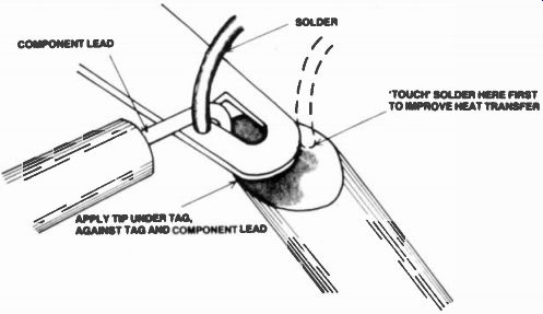
Fig. 12. When soldering a component to a tag, apply the iron to the tag and the
lead to heat them up. After a few seconds, touch the solder on the iron
briefly and then apply the solder to the join.
Figure 12 shows how to solder a component lead to a tag. Apply the iron to the tag as the tag has the greatest mass. To improve heat transfer and reduce soldering time, first apply a little solder to the iron at the junction of the bit and the tag. Just a touch is sufficient. The flux removes any tarnish from the tag and the hot solder tarnish that forms on the face of the bit, allowing rapid heating of a small area. The molten solder improves the thermal contact by wetting both surfaces and filling the minute air spaces between them. Next apply the solder to the tag. The solder will only melt if the tag is at the correct temperature, thus ensuring proper wetting.
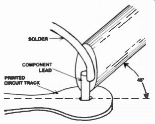
Fig. 13. When soldering a component lead to a printed circuit board,
apply the iron to the lead with the tip touching the copper track as
well.
Soldering components to a printed circuit board is shown in Fig. 13.
Always take care not to overheat printed circuit boards as the copper track may lift, damaging the board and making subsequent connections difficult.
Always hold the iron on the joint for a second longer after sufficient solder has been applied. This ensures that all the solder is melted and that the flux has been de-activated. Allow the solder to cool naturally. Don't blow on it to cool it. Don't move the joint while the solder is solidifying--a poor joint may result.
Take care not to apply too much solder as it may conceal a poor joint.
On printed circuit boards, too much solder may cause 'solder bridges' to form between tracks.
How much is the right amount of solder, and what does a good joint look like?
The size of the solder 'fillet should be large enough to fill the area of the joint and the contours of the parts should be plainly visible. The surface of the solder should be smooth and bright and meet the parts of the joints at a tangent. This 'feathering' indicates good wetting. The characteristics of a good joint are shown in Fig. 14.
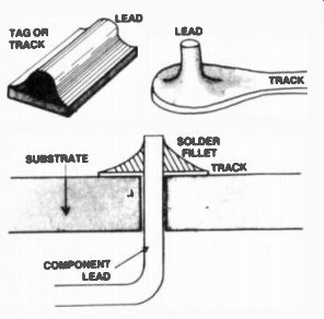
Fig. 14. A good joint will be covered by a small fillet of solder which
meets the parts of the joint at a tangent. The solder should be smooth
and bright.
There must be sufficient solder filling the spaces of the joint to ensure a good mechanical bond. Insufficient solder results in a mechanically weak joint. The joint is likely to go open circuit or intermittent under slight mechanical stress (such as due to vibration or expansion and contraction with temperature changes). Joints having insufficient solder are shown in Fig. 15.
Fig. 15. Insufficient solder leads to a weak joint which may become
faulty.
The Problem Of Plated Through Holes
Double-sided PCBs with plated-through holes are becoming increasingly common. It is important that the correct technique be used to solder components to the board as well as when desoldering component leads.
In general, one can solder component leads from the component side of the board. The usual rules, as described here, about applying the iron to the lead and the track apply.
Likewise with the appearance of the joint. Component leads should not be crimped or clinched as it is unnecessary. A properly made joint is illustrated in Fig. 16. The application of too little solder will result in a joint as illustrated in Fig. 17.
When desoldering leads from a through-plated hole, as much solder should be removed from the joint as possible. Vacuum-operated desoldering tools are best for this purpose.
However, the lead should be removed while the iron is still applied to the joint and the solder is molten. Otherwise, you may damage the through-plating in the hole. The iron should not be pressed hard onto the pad as this too can result in damage to the through plating. With ICs and/or IC sockets where a number of joints have to be de-soldered simultaneously, special desoldering tool bits can be obtained, or else the pins of the package must be cut, destroying it.
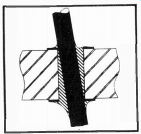
Fig. 16 A properly made joint in a plated through hole.
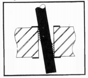
Fig. 17 Too little solder results in weak joint that may fracture and become intermittent
or unreliable. When desoldering, a little solder will always adhere
to the joint inside the hole in the positions shown, so the lead must
be withdrawn while the solder is molten.
Bad Joints And How To Cure Them
In some instances, the solder may not wet the joint evenly. The solder surface is not smooth and continuous, having irregular, round, non-wetted areas exposed. The solder may meet one surface abruptly in places. This condition is illustrated in Fig. 19. It can often be remedied by reheating, although desoldering and cleaning may be necessary in some cases.
When a joint is not wetted at all, usually due to tarnish, the solder will not completely cover the surface and appears as droplets or balls (Fig. 20). This is a bad joint mechanically and electrically and should be taken apart and properly prepared.
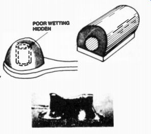
Fig. 18. Too much solder can hide poorly wetted surfaces (top left),
which results in a poor joint. On PCBs with close conductor spacing too
much solder leads to 'bridging' (bottom).
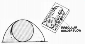
Fig. 19. When poor wetting occurs, the solder meets one surface at an
abrupt angle and the solder flows irregularly.
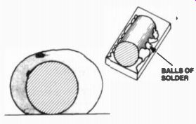
Fig. 20. Tarnished surfaces prevent wetting altogether. Ball of solder
sit on the surface.
Sometimes during soldering, the molten solder will run along the metal and then withdraw towards the fillet when the iron is removed (Fig. 21).
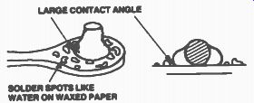
Fig. 21. De-wetting. The solder appears to flow properly, then withdraws
when the iron is removed from the joint.
This 'de-wetting' is another problem caused by tarnish that the flux is unable to remove. The joint has to be de-soldered and thoroughly cleaned before resoldering. Applying more heat and excess solder may make the joint look all right but it may conceal a bad joint.
A 'cold' or 'dry' joint is usually caused by movement of the parts during soldering or as the solder is solidifying. It is also caused by the solder running onto surfaces cooler than the soldering temperature. A cold joint has a frosty appearance, as shown in Fig. 22, but may otherwise look like a good joint. The trap with cold joints is that they may perform quite well for a considerable period and then suddenly become intermittent or go open circuit. They are repaired quite simply by reapplying heat or desoldering the joint and then resoldering.
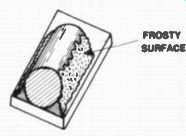
Fig. 22. A 'cold' joint. The solder surface has a frosty appearance
but looks good otherwise.
If insufficient heat is applied to a joint, the solder solidifies before adequate wetting occurs, causing the angle of contact between the solder and the parts to be very large. The flux is not properly activated and the joint may tarnish. The solder can usually be pried loose. The surface of the solder may be smooth and continuous but it is not attached to the parts of the joint (Fig. 23). Reheat the joint if tarnishing is not evident, otherwise desolder and clean before soldering.
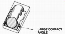
Fig. 23. Too little heat. The solder forms a large contact angle with
the surface and can be prised loose.
In some cases, a resin bond is formed between the parts of a joint. In this case, the angle of contact of the solder is usually large and a layer of solidified resin forms the bond, as shown in Fig. 24. There may be no electrical contact at all, the joint has little strength and may be prised apart.
It may be caused by excess flux or solder running onto surfaces cooler than soldering temperature but hot enough to melt the flux. It is usually cured by reheating the joint, making sure that all parts are brought up to soldering temperature.
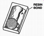
Fig. 24. A resin bond. There may be no electrical contact at all. It
can be cured by reheating the joint.
When soldering multi-strand hookup wire, excess solder or long soldering time can cause solder to run along the strands. This is called 'wicking' (Fig. 25) and can be reduced by soldering faster or by using a heatsink on the wire. Wicking makes the wire brittle and liable to break when it is moved.
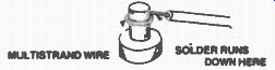
Fig. 25. 'Wicking' is caused by solder running back up multistrand hookup
wire.
This makes the wire brittle at the joint and movement may break it.
When the soldering iron is withdrawn from a joint a spike of solder, called an 'icicle', is sometimes left behind, usually pointing in the direction in which the iron was removed (see Fig. 26). Icicles may be caused by a variety of problems, including tarnished joints, too short soldering time, low soldering temperature or excess solder on the iron. Reapplication of the soldering iron usually remedies the problem, but make sure that there is not some other problem with the joint. If the joint is otherwise sound, small icicles are nothing to worry about.
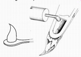
Fig. 26. 'Icicles sometimes form on a joint when you remove the iron.
Reheat the joint with a clean tip to get rid of them.
Preparing Leads and Components
Most modern components have leads which are tin-plated to aid soldering.
The tin is readily absorbed into the solder, allowing rapid wetting and reducing soldering time. The plating will tarnish with time and handling.
Unplated leads and unprotected printed circuit boards are particularly affected as oxidization is quite rapid.
It is always a good practice to tin the parts of a joint before putting them together. Component leads can be tinned by simply heating them with the iron and then applying a little solder.
Only tin that part of the lead that is actually going to make the joint as component leads are usually trimmed after the joint is made. If the lead is tarnished, it can be cleaned by pulling it through a doubled-over piece of emery cloth or plain steel wool. Printed circuit board tracks do not need tinning. If the tracks are tarnished, clean the board with an abrasive powder cleanser (such as Ajax) and a moist cloth. Wash the board in clean water after cleaning and dry with a tissue or paper towel.
Stranded hookup wire is best prepared in the following manner. Strip away about 6-7 mm of insulation from each end. Twist the strands together, apply the hot iron for about one second and then a touch of solder. Don't overheat or apply too much solder.
Solid hookup wire is prepared the same way as component leads.
Tarnished tags are best cleaned by rubbing with emery cloth or lightly scraping them with a penknife.
Thoroughly heat the tag with the iron before applying a little solder to tin it.
Enameled coil wire can be prepared by stripping the end back about 6-10 mm using a penknife, cutting blade, emery cloth or steel wool until the bright copper wire shows. Tin it quickly. Some modern coil winding wire is coated with an enamel that, although very tough, melts at soldering temperatures ('Bicalex' and 'Lewmex' are several trade names). A hot soldering iron is applied to the end to heat it first. Apply some solder to the face of the iron then to form a molten blob to cover the wire. Shortly, the insulation will smoke and burn off, allowing the wire to be tinned. A good hot tip is necessary for this operation.
Mounting Components on Terminals
There are good and bad ways of attaching component leads to terminals before soldering. The correct method of attachment depends on the type of terminal. Pins are generally meant to have the lead bent around them, other terminals have holes through which the component lead is inserted. The main principle to keep in mind is that the lead must always be easy to remove if subsequent servicing or modification is necessary. Also, the solder should not provide all the mechanical support for the component.
Terminal Pins are often used with matrix board, being inserted into the holes at convenient positions. The component lead should be bent around the pin, making an angle of approximately 135°, as shown in Fig. 27 (left). If the angle is too small, the connection is mechanically weak--it depends too much on the solder. If the lead is wrapped right around the terminal it is difficult to remove (Fig. 27, right).
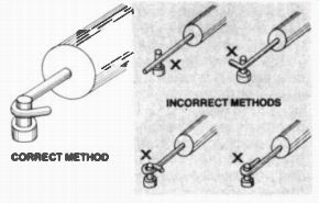
Fig. 27. How to attach a component lead to a terminal pin before soldering.
When mounting a component between two terminal pins, first bend each lead at the point corresponding to the position of the terminal, leaving sufficient slack in each lead for a little movement in the component. Tension each lead against the terminal during soldering (Fig. 28).
BEND LEADS TO PROVIDE SLACK
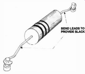
Fig. 28. When mounting a component between terminal pins leave a little
slack in the leads Solder Tags and Terminals with Holes are found on
tagstrips, potentiometers, switches, etc. The best methods of connecting
leads to them are shown in Fig. 29b. In each case, there is adequate
contact between the lead and terminal and the lead can be easily removed
if necessary later. Do not wrap the component lead right around the terminal
as this makes subsequent removal difficult and messy, but if the lead
is not bent around the terminal at all too much dependence is placed
on the solder for both mechanical and electrical connection. The wrong
ways are illustrated in Fig. 29b.
The way a component is mounted between two terminals of this type depends on the orientation of the terminals. Where the holes are approximately parallel, bend each lead at right angles at the point corresponding to the position of the terminal hole. The lead is inserted without further bending (Fig. 301.
Leave a little slack in the leads for movement. Hold the lead firmly when soldering.
Where the terminal holes are in line lie coaxial), bend one lead around one terminals as illustrated in Fig. 29 and pass the other lead through the other terminal without bending it. Solder the bent lead first. Tension it against the terminal while soldering. Arrange a little slack in the leads before soldering the renaming lead (Fig. 31a). If the terminals are at a slight angle to one another, form one lead to pass along the side of the terminal closest to the body of the component before entering the hole. Don't bend it further. Pass the other lead through the other terminal hole without bending it either. Solder the bent lead first, tensioning it against the terminal to prevent movement.
Again arrange a little slack in the leads before soldering the remaining lead.
(Fig. 31b).

Fig. 29. The best way to attach component leads to tags and terminals
(left).
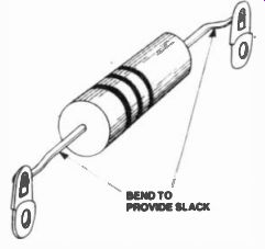
Fig. 30. Mounting a component between tags with parallel holes.
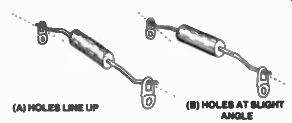
Fig. 31 Mounting component leads where the tag holes line up, or nearly
so. Bend the leads to provide some slack.
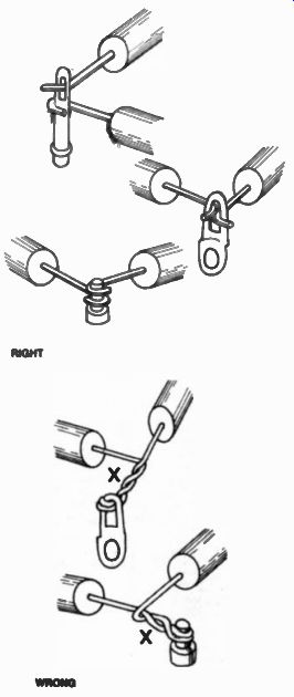
Fig. 32. When several component leads go to one terminal, attach each
lead separately.
Fig. 33. When mounting components to a printed circuit board, the leads
may be splayed, before soldering, to hold them in position.
To mount a component between a terminal pin and a solder tag, bend the leads around each terminal according to the principles outlined above.
When terminating several leads on one terminal, each lead should be connected separately, regardless of the type of terminal. This allows any single component to be easily removed. Don't twist the leads together as this prevents subsequent removal. Figure 32 illustrates the correct and incorrect methods of terminating several leads to one terminal.
When interconnecting two terminals use a length of wire between them.
Don't use component leads.
Mounting Components on Printed Circuit Boards
Components should always be mounted on the non-copper side of a printed circuit board, unless especially noted otherwise. The component leads should be inserted in the correct holes and may be formed in a variety of ways before soldering. The leads may be splayed, as shown in Fig. 33, to hold the components in position before soldering. This method allows all the components to be mounted before soldering. See Fig. 34.
Another method is to mount the components one at a time, cutting the leads close to the board before soldering, as in Fig. 35. However, this necessitates holding the component steady whilst soldering.
For a neat appearance, do not leave excessive lead length on the components; place them against the board and align them parallel to an edge. Generally, printed circuit boards are laid out so that the components will lie parallel to an edge when correctly inserted. It is a good idea to position the components so that their value and voltage rating or type number can be seen. This greatly facilitates checking and later servicing.
BEND LEADS FLAT PC TRACKS
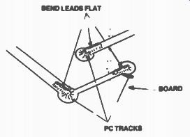
Fig. 34. The leads may be cut off and bent to lie flat along the track
on the board and than soldered.
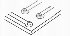
Fig. 35. Alternatively, the leads may be cut so that they protrude a
short way, and then soldered. They may be cut off after soldering if
you wish.
Sometimes components are mounted vertically. It is best to splay or clinch the leads in this case and allow a small clearance between the end of the component closest to the board and the board. Vertically mounted components are illustrated in Fig. 36.
Many capacitors, ceramic capacitors particularly, have their coating material extending a little way down the leads.
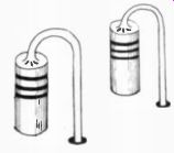
Fig. 36. Whilst axial lead components lie resistors) are generally mounted
horizontally on a PCB, they are sometimes mounted vertically. Leave a
millimeter or so clearance between the bottom end and the board.
This should not be removed beyond the point where the leads enter the component body. The coating should not enter the hole in the printed circuit board. Where double-sided board is used, allow a clearance of 2 mm or so between the circuit pad and the coating on the lead.
Components with metal bodies that are mounted on the copper side of a board, or on double-sided board, or that cross a track or jumper lead should be sleeved or otherwise insulated to prevent a short circuit.
Precautions with Semiconductors
Most semiconductors are damaged by overheating. Always solder or desolder semiconductors quickly and cleanly.
Make sure all parts to be joined are clean and/or tinned beforehand. If you don't feel confident about making the joint quickly, use a heat shunt leg a pair of pliers) between the end of the lead being soldered and the transistor body to divert the heat. Special heatsink tools are obtainable for this purpose.
Integrated circuits require particular care when being soldered into printed circuit boards. If too much solder is applied, a 'solder bridge' may form between adjacent pins (see Fig. 18). This necessitates removing the solder, with the risk of damaging both the board and the component.
Transistors and integrated circuits of the MOS or CMOS type are easily damaged by electrostatic charges or leakage currents from the soldering iron. These devices are normally supplied with their pins inserted into a conductive material, usually a black foam. Leave them in this until they are to be used. Avoid touching the pins, as even small static discharges from the body (caused by clothing) can cause damage.
Always fit MOS or CMOS components last. Insert the device into place quickly. Solder the power supply pins first. The devices are built so that this activates built-in protective circuitry. The remaining pins may then be soldered with little chance of damage. Sockets for ICs are worth using as they remove the necessity of soldering directly to the IC pins, thus reducing the possibility of damage.
To reduce leakage currents produced by a soldering iron, connect a flexible lead from the metallic part of the iron (make sure it connects to the tip) to an alligator clip that can be attached to the equipment earth 10 V rail). Soldering irons that use a step down transformer should have an earthed electrostatic shield between the windings. It is wise to check this when buying. Alternatively with an iron that has sufficient heat capacity, disconnect the iron when soldering components that are sensitive to leakage currents.
Desoldering
Where joints have to be de-soldered there are two basic methods that can be used to effectively remove the solder--'soaking' it up and sucking it up.
It is possible to remove leads while the solder is molten by just heating the joint. However, this is not the best method, as a component may be damaged by the amount of heat produced. Also, flexing the leads whilst trying to remove the component may damage the lead or the lead-body seal.
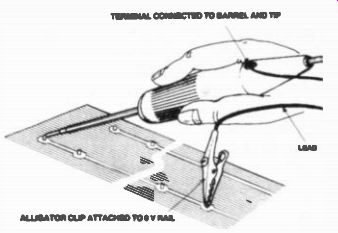
Fig. 37. A precaution to take when using mains-operated or unprotected
low-voltage irons on MOS components is to connect the metallic part of
the iron to the 0 V rail of the equipment with a clip lead.
A terminal or printed circuit can also be damaged by heat or attempts to prise the component loose while the solder is molten. It is much better to use a desoldering aid.
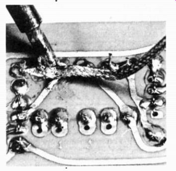
Fig. 38. How to use desoldering wick. Lay it over the joint and apply
the iron tip to the braid, using a little pressure. When the solder is
drawn into the braid, remove the iron and the braid.
Desoldering 'wick' can be used to soak up molten solder from a joint. This consists of a copper braid impregnated with resin. When applied to a joint and heated with a soldering iron, molten solder from the joint flows into the fluxed braid by capillary attraction, effectively clearing the joint of solder.
Figure 38 shows how it's done.
You lay the wick over the area to be de-soldered. The iron is applied to the wick and some pressure applied. As the wick heats up it activates the flux in it, which flows onto the joint, and as the solder on the joint melts it replaces the flux in the wick, flowing into the braid quite quickly. The 'used' wick is cut off afterwards. A tip running at a higher temperature and having more heat capacity than generally used for soldering is recommended. Desoldering wick is excellent for general use and on joints having a large area.
Sucking up the solder with a suitable tool is a very effective method. Hand-held 'solder suckers are inexpensive and popular but a variety of desoldering irons with suction devices incorporated are also available.
Solder suckers have a spring-loaded plunger in a barrel with a thumb operated release mechanism. A heat resistant nozzle at one end is applied to the joint, which is heated with an ordinary soldering iron. When the plunger is released, molten solder from the joint is drawn into the barrel. Figure 39 shows how it's done. They are excellent for general use with PCBs boards.
Fig. 40. This Hakko 'Vac Ace' desoldering tool from G.E.S. employs a
small vacuum pump to draw molten solder from the joint into the glass
barrel atop the gun handle. A steel wool wad absorbs the solder. This
tool is particularly effective on through-hole plated PCBs
Fig. 39. Using a hand-held solder sucker. The nozzle is made of Teflon
IPTFE), a heat resistant plastic, and is replaceable. To use it, load
the plunger in the tool. Heat the joint until the solder melts, apply
the sucker's nozzle to the joint and release the plunger.
That's the general technique, and it's fine for equipment using bipolar devices, but it can be extremely dangerous for MOS devices. A US maker of solder suckers, Anderson Effects, points out that standard plastic solder suckers have been found to produce a static surge of 5 kV to 10 kV at the tip. This is invariably in contact with the device's leads when the surge occurs and may damage or destroy the device. To obviate the problem static free metallized plastic nozzles may be obtained. Otherwise, use desoldering wick or a vacuum-operated desoldering iron.
A variety of desoldering irons having a hollow tip through which the molten solder is drawn by a vacuum pump are available. These are particularly useful for servicing work. An example is shown in Fig. 40.
Material for preparing this article was derived fro m Australian Post Office technical training publication ETP 0276, 1972, and The Art of Soldering, ETI April 1975 Additional material and photographs were kindly supplied by Royston Electronics, Multicore Solders Pty Ltd, The Cooper Tool Group Ltd, Scope Laboratories and General Electronic Services.
(adapted from: Hobby Electronics magazine, Feb. 1982)
Also see: