Operating a relay to switch heavy current or mains voltages is a common application. This project permits a relay to be switched in a variety of ways, from a variety of inputs.
THIS VERSATILE relay driver unit is intended to be used with projects or devices not normally providing a switched relay output. In addition, power for external circuitry can be obtained from the board.
The unit has three groups of 'logic' inputs and a direct input. The relay itself is driven by two transistors, Q1 and Q2, and the direct input goes to the base of Q1 via a resistor (R7). Linking this input to the unit's 0 V rails- via a switch, a transistor which is turned on by a signal (open-collector logic) or a logic gate output--will operate the relay.
The logic circuitry on the board can be implemented by installing Link 1, which connects the output of the logic circuitry to the direct input. There are two 'logic high to operate' inputs (pins 1 and 2). A logic high level--ie a voltage level above about 2V--on either of these inputs will operate the relay. There are also two 'logic low to operate inputs (pins 7 and 8). Pulling either of these inputs below logic low--about 0V5--will operate the relay.
Note that these input pairs are ORed with diodes and can be linked so that one input inhibits the other. In addition there are two 'latch' inputs, pins 3 and 5. Pin 4 is the output of the latch circuitry and latch operation is implemented by linking this pin to one of the other inputs. All the logic inputs are high impedance and can be driven from CMOS circuitry.
The unit is powered from a 12 to 15 V AC source such as a battery or 5 VA transformer. Supply for IC1 (and perhaps any off-board circuitry) is obtained from a simple zener regulator circuit. This can be chosen to suit individual requirements. We used a BZX61C/8V2 zener to provide an 8V2 rail for IC1, and a 220 ohm, 1W resistor for R5. You can use any convenient zener from 5VI to 15 V--but no higher, and we recommend 1W types run at around 50-60 mA current.
You will have to work out the value of R5 according to your choice of zener.
For a 15 V zener, R5 could be 47 ohms, for a 5V1 zener, 270 ohms, or for a 12 V zener, say 100 ohms.
There's plenty of latitude and these values are only given as a guide.
The logic circuitry lie IC11 can be supplied from an off-board source if you wish. To do so, remove R5 and use a 15V zener for ZD1 to prevent spikes on the external supply line causing damage to IC1. Note also that the logic levels on inputs 1, 2, 3 and 5 should also be no higher than 15 V. The accompanying drawings illustrate how the unit is used in its four basic modes of operation.
Construction
Construction is very straightforward. The components may be mounted in any order but you will probably find it easiest to leave the relay and C1 until last. Watch the polarity of all the diodes, the transistor and the IC. However, leave out Link 1 at this stage.
Once you've got it together and have checked everything, apply 12 VAC to the AC input and check various modes of operation as follows: (1) Bridge the free end of R7 to ground.
The relay should operate.
12) Install Link 1, then bridge pin 7 to ground. The relay should operate.
Likewise for pin 8.
13) Bridge pin 1 to the cathode of the zener. The relay should operate.
Likewise for pin 2.
14) Connect pin 4 to pin 1 or 2. The relay may operate. Apply a pulse to pin 3 or 5 and see that it latches on. A pulse on the other input will drop it out again.
If all is well, you unit is ready for installation!
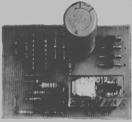
--- The relay driver board is simple, yet versatile. The external input/output
pins are located around the edges of the board.
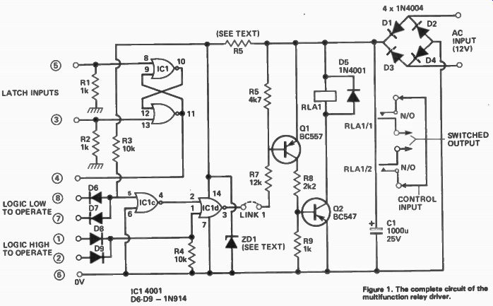
Figure 1. The complete circuit of the multifunction relay driver.
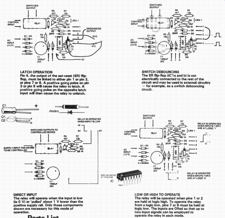
LATCH OPERATION--Pin 4, the output of the set-reset (SR) flip flop, must be linked to either pin 1 or pin 2, or pins 7 or 8. A positive-going pulse on pin 3 or pin 5 will cause the relay to latch. A positive going pulse on the opposite latch input will then cause the relay to unlatch
SWITCH DEBOUNCING--The SR flip-flop (IC1a and b) is not electrically connected to the rest of the circuit and may be used in external circuitry- for example, as a switch debouncing circuit
DIRECT INPUT--The relay will operate when the input is low (ie 0V) or 'pulled' about 1 V lower than the positive supply rail. Only those components shown are necessary for this mode of operation.
LOW OR HIGH TO OPERATE--The relay will be operated when pins 1 or 2 are held at logic high. To operate the relay from a logic low, pins 7 or 8 must be held at logic low
The inputs are ORed so that up to two input signals can be employed to operate the relay in each mode
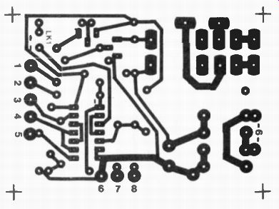
Figure 2. Bottom view of the PCB make it yourself.
------------
How It Works
The best place to start is right in the middle of the circuit--because that's the 'business' end! Transistor Q2 has relay RLA 1 as its collector load. Diode D5 provides protection for Q2 when the coil cur rent is cut off whenever Q2 is turned off. The base of 02 is driven by the collector of Q1 via R8 and R9. Base bias for Q1 is obtained from the resistor network of R6 and R7. The 'free' end of R7 can be linked to on board logic circuitry (IC1 or driven by an external source.
If the free end of R7 is connected to 0V then base current will flow in Q1 which will turn on. This will turn on Q2 and the relay will operate. In fact, all that is required to turn Q1 on is to 'pull' the free end of R7 about 1V below the positive supply rail to overcome the 0V6 base-emitter turn on voltage of Q1.
Effectively, a low' level on the free end of R7 will operate the relay.
Two groups of logic circuitry built around IC1 are included to provide a variety of operating 'modes'. IC1 is a quad NOR gate package. One gate, IC1d, is arranged to provide a 'logic high to operate' mode. Two diodes connected as simple OR gate have their cathodes connected to pin 1 of IC1 d. The output of another gate, IC1 c, drives the other input, pin 2, of IC1d. IC1 c has one input (pin 6) connected to 0 V, which is thus held at logic low. Pin 5 IC1 c is held at logic high by R3 and thus its output, pin 4, will be low. As this drives pin 2 IC1d, its output (pin 3) will be high. With Link 1 fitted, Q1 will normally be off and the relay not operated.
When a high logic level is applied to either input pin 1 or 2, or both, the diode(s) will conduct driving pin 1 IC1d high. The output, pin 3, will go low and the relay will operate. The relay will remain operated only while the input remains high.
Two diodes (D6, D7) are connected as a simple OR gate with their anodes connected to pin 5 IC1 c. A logic low on either input pin 7 or 8 ('logic low to operate') or both will pull pin 5 IC1 c low and its output, pin 4, will go high. Pin 2 IC1 d will go high and thus pin 3 IC1 d will go low and the relay will operate. The relay will remain operated only while the input remains high.
The remaining two gates from (C1 are connected as a set-reset (SR) flip flop. Pin 4 on the printed circuit board provides an output which may be coupled to the other inputs. Assume the SR flip output is initially low. A pulse applied to input pin 5 will cause pin 4 (pins 9, 11 or IC1 a, b) to 'latch' high. A pulse then applied to the opposite input pin will cause the output to go low again and remain low.
This part of the circuit can be used as a 'switch debouncer' as illustrated.
Power is derived from an off-board 9 VAC or 12 VAC source. This drives a bridge rectifier, diodes D1 to D4, smoothing being provided by C1.
A zener diode, ZD1 , is used to provide a regulated supply to the logic circuitry (IC 1).
Buylines
There should be no problems with any of the components used in this project--they are all easy-to-obtain types. The PCB-mounting relay is type RL111 from Watford Electronics, whose address can be found elsewhere in this issue.
-------------
Parts List
RESISTORS (all 1/2 W, 5% unless noted)
R1, 2, 9 1k0 R3,4 10k R5 220R, 1W (see text)
R6 4k7 R7 12k R8 2k2
CAPACITORS
C1 1000 u, 25 V electrolytic (PCB mounting)
SEMICONDUCTORS
IC1 4001 B
Q1 BC557
Q2 BC547
D1-D5 1N4001, 1N4002 etc
D6-D9 1N914, 1N41 48 etc ZD1 400 m W or 1 W zener, see text
MISCELLANEOUS
PCB; RLA1--relay (type RL 11)
(adapted from: Hobby Electronics magazine, Feb. 1982)
Also see:
DIY Project--Digital Capacitance Meter