In 1957, a revolutionary incident occurred in the world of electronics: the invention of the integrated circuit (abbreviated JC) by Jack S. Kilby at Texas Instruments, Inc. (In 1969, Mr. Kilby received the National Medal of Science.) The IC ushered in the present age of microelectronics by offering on a single, tiny, semiconductor wafer an entire circuit including diodes, transistors, resistors, capacitors, and internal "wiring." In the decade that followed its relatively quiet introduction, the IC found application in all kinds of electronic equipment, from space vehicles to TV receivers.
An entire circuit can now be plugged in and out of a system in the same way that a single transistor formerly was. Some times, an external component or two will be needed, but often only a DC supply is required to make an IC work.
This section describes the IC and explains in simple language the highlights of IC fabrication and operation.
1. WHAT IS THE IC?
In many respects, the IC is a refined and sub-miniaturized version of the early electronic module. The reader will recall that the module was a complete circuit (such as an amplifier, flip-flop, oscillator, or detector stage) made as small as possible and provided with a plug-in base so that it might quickly be inserted into or removed from a larger circuit or system (receiver, transmitter, test instrument, computer, etc.). Modules enable an experimenter or designer to bread board a large setup with a minimum of effort, since they provide ready-made stages; they also speed up maintenance, by allowing an entire defective stage to be replaced quickly and repaired at leisure.
The first modules used tubes and were monstrous by present-day standards of size. Then came transistorized modules, which were much smaller. Next, printed-circuit techniques resulted in further size reduction and improved uniformity. Finally, the IC took the stage as a microminiature module. An IC no larger than a small-signal transistor, and even resembling the latter in size and shape, can contain a number of diodes, transistors, capacitors, and resistors, plus all of the interconnections between these components needed to provide a complete circuit. Various input, output, dc power, and auxiliary connections are made to appropriate points in the tiny circuit and are run to pigtails or lugs for external connection. In the design of the early tube- or transistor-type modules, the goal was to make components as small as possible, wiring as compact and simple as practicable ( even fastening the terminals of some components together to avoid interconnecting leads), and packing the components together as tightly as practicable. In the IC, however, all of the components and interconnections are fabricated by processing appropriate areas of a single-crystal semiconductor chip or wafer, the whole being kept to microminiature size.
It is beyond the scope of this introductory guide to explain in extensive detail how a commercial integrated circuit is manufactured; however, a reasonably clear idea of the general process and of the final structure can be gained from the following section.
2. INSIDE THE IC
For a picture of the general nature and fabrication of the IC, refer to Figs. 1 to 4. In each instance, the wafer is doped silicon, which provides the substrate into which the various components are produced by diffusion, and the bold black areas represent metallic contacts that are deposited on the surface.
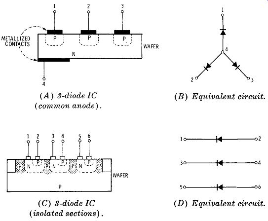
Fig. 1. Basic integration: diodes.
Integrated Diodes
In Fig. 1A, the wafer contains three diodes. Each of these consists of a small diffused p-type region forming a junction with the n material of the wafer. Each of the p regions thus makes a diode with the common n region sup plied by the substrate. Thus, the n-type wafer not only supplies the substrate which supports the diodes, but also acts as a common cathode for all three diodes (see the equivalent circuit in Fig. 1B). Although, for easy illustration here, the metallized contacts are shown as having simply been deposited on the surface of the wafer over the proper areas, the arrangement usually is not this simple. Instead, as shown in Figs. 3 and 4, a thin oxide layer or film is formed over the diffused areas to protect them; then this film is properly etched to allow contact with the specific areas, and finally the metal is deposited on top of the oxide.
(Note in Fig. 4A, for example, how the metal has penetrated through etched slits in the oxide at points 6 and 7 to make contact with the n and p regions, respectively, of the diode underneath.) In a structure such as that shown in Fig. 1A, some leak age of current will occur through the substrate between the components (diodes here). However, the resistivity of the substrate is high, and the leakage currents are consequently low. Nevertheless, techniques for isolation of integrated components have been worked out. One such arrangement is shown in Fig. lC, in which a high-resistance p region has been diffused into the wafer between diodes.
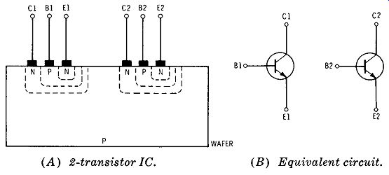
Fig. 2. Basic integration: transistors.
Unlike the common-anode arrangement of Fig. 1A, the three diodes in Fig. lC have individual, separated anodes.
For each diode, an n region (for the cathode) first is diffused into the wafer, and then a p region (for the anode) is dif fused into the n region. The three diodes (see equivalent circuit in Fig. 1D) then may be connected in any way the user desires.
Integrated Transistors
Fig. 2A shows how the technique just described is extended to produce transistors in the substrate. Here, an n region first is diffused (for the collector electrode of the transistor) into the substrate. Next, a p region (for the base) is diffused into this n region. And finally, an n region (for the emitter) is diffused into this base p region. The result is an npn transistor. When the collector is situated adjacent to the substrate, as it is in Fig. 2A, the substrate bulk can aid in the removal of heat from the collector.
While, for easy illustration, the metallized contacts are shown as having simply been deposited on the surface of the wafer over the collector, base, and emitter areas, the arrangement usually is not this simple. Instead, as shown in Figs. 3 and 4, a thin oxide layer or film is formed over the surface of the wafer for protection; then this layer is properly etched to allow contact with the specific areas, and finally the metal is deposited on top of the oxide. (Notice in Fig. 4A, for example, how the metal has penetrated through etched slits in the oxide--at points 8, 9, and 10--to make contact with the n-, p-, and n-type regions that constitute the transistor underneath.) A number of transistors might be processed into the wafer, consistent with the size of the wafer, but for simplicity only two isolated ones are shown in Fig. 2A. The equivalent circuit is given in Fig. 2B. Although simple bipolar transistors are shown here, FETs and MOSFETs also are found in integrated circuits, and power transistors are found as well as small-signal ones.
Integrated Passive Components
Resistors and capacitors also may be processed into the IC wafer. Fig. 3A shows the formation of a resistor. Here, the metallic electrodes (a, b) make contact with the diffused p region that constitutes the resistor "material." (Suitable control of the chemical composition of this p region deter mines the amount of resistance.) The surrounding diffused n region forms a diode with the resistive p region to isolate the integrated resistor from other components integrated into the same substrate. Fig. 3B shows the equivalent circuit.
Fig. 3C shows the formation of a capacitor. Here, one metallic electrode (a) makes contact with the diffused n region, which acts as one plate of the capacitor. The other metallic electrode (b) is deposited on top of the oxide layer, directly over and facing most of the n-region area, but not extending through to that area, and forms the second plate of the capacitor. The oxide layer between electrode band the n region serves as the dielectric separator of the capacitor.
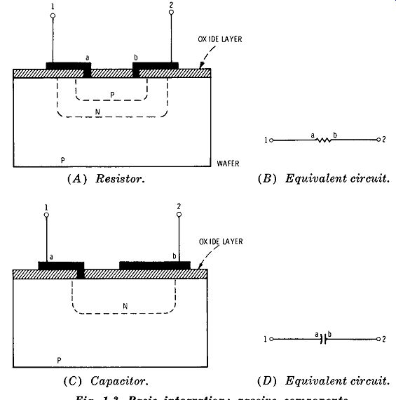
Fig. 3. Basic integration: passive components.
As in other capacitors, the capacitance depends upon plate area, dielectric thickness, and dielectric constant. Fig. 3D shows the equivalent circuit.
At this writing, techniques for the microminiaturization and integration of inductors have not been completely successful. Therefore, external coils, transformers, and chokes are now being used with ICs. Some promise is offered, however, by the gyrator, an active device which under certain circumstances can make a capacitor (which, of course, can be integrated) look like an inductor. The gyrator is essentially a special, multi-transistor, direct-coupled, negative feedback amplifier (itself easily capable of integration).
Integrated Complete Circuit
Fig. 4 shows a full circuit containing both active and passive components integrated into a single p-type wafer.
While this circuit is not necessarily functional, consisting as it does of three components connected in series, it is illustrative of the method and configuration of the integrated circuit.
The individual components (from left to right in Fig. 4A: 1 capacitor, 1 resistor, 1 diode, and 1 transistor) were separately described in the preceding discussion. The components are "wired" in series by having the deposited metallic electrodes run between, and make contact with, the individual components. Fig. 4B shows the equivalent circuit, with the identifying numbers matching those in Fig. 4A. From this rudimentary illustration, it should be easy to visualize a multistage amplifier circuit consisting of several properly connected transistors, bias resistors, coupling capacitors, load resistors, and voltage-stabilizing diodes, all integrated into a single wafer.
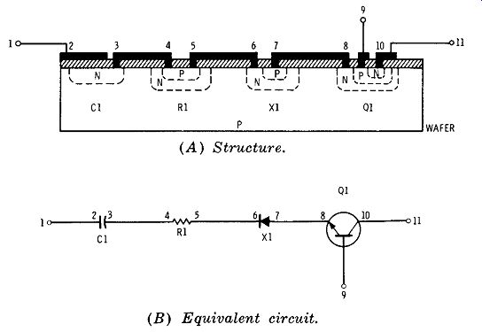
Fig. 4. Basic integration: complete circuit.
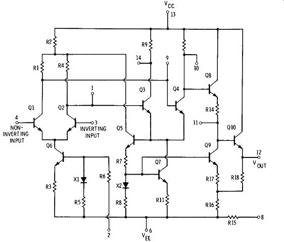
Fig. 5. Typical integrated circuit: RCA Type CA3030.
Typical ICs
For some idea as to the component content of a typical integrated circuit, see Fig. 5. This is the internal circuit of the RCA Type CA3030 operational amplifier IC. In this unit, there are 10 transistors, 2 diodes, and 18 resistors (30 components and all the internal "wiring" on a chip a few mils square). This IC has two inputs (terminals 3 and 4) and one output (terminal 12). Its frequency range is DC to 50 MHz, and its voltage gain is 70 dB. As is seen from Fig. 5, a number of terminals are provided. This enables the user to use a part of the internal circuit, as well as the entire IC. For some idea of the appearance of an IC chip, see Fig. 6.
In this photograph, the monolithic chip has been magnified approximately 30 times. This IC is a Fairchild Type LPDTµL 9040 clocked flip-flop containing 16 transistors, 16 diodes, and 22 resistors, and is used in counters, shift registers, and other computer and calculator devices. Notice the wire leads running out from various circuit points. When this IC is packaged, its plastic housing is only approximately ¼ inch square and less than ½ inch thick.
From the foregoing descriptions in this section, the reader will find the Electronic Industries Association's definition of the integrated circuit a relevant one: "The physical realization of a number of electrical elements inseparably associated on or within a continuous body of semiconductor material to perform the functions of a circuit."
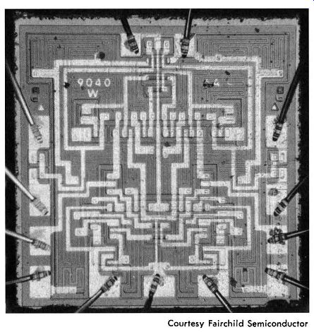
Fig. 6. A monolith IC chip magnified approximately 30 times. The IC is a
clocked flip-flop circuit containing 16 transistors, 16 diodes, and 22 resistors.
3. CLASSIFICATION OF ICs
Integrated circuits may be classified in a number of ways. The most useful classifications are (1) according to construction, (2) according to operating mode, and (3) according to packaging. These are discussed separately in the following paragraphs.
According to Construction
Depending upon construction, ICs are described as monolithic, thin film, or hybrid. The monolithic IC is the most common type and is DC scribed in the foregoing discussions. All of its components and interconnections are formed in a single chip or wafer of semiconductor material. Throughout its body, however, the chip is one material, various small areas of it having been processed to afford diode, transistor, capacitor, or resistor action. It is this feature that suggests the term monolithic (from the Greek monolithos, "made from one stone"). Be cause of this one-material/ one-block construction, high uniformity and reliability are obtainable ( e. g., the user is easily guaranteed matched diodes and transistors). In the thin-film type of IC, suitable materials (such as semiconductors and metals) are deposited in thin-film form on the semiconductor chip as substrate. Then the resulting special areas are processed to achieve complete integration and desired electrical characteristics. It is somewhat as if the circuit, components, and wiring were printed on the semi conductor substrate and then blended into the latter. Transistors, however, are not usually formed in ICs by this process. It should be mentioned here that thick films also are used sometimes.
The hybrid type of IC combines features of both the monolithic and film types. Sometimes, the term hybrid is applied also to units that contain two or more interconnected IC chips. Other terms occasionally used to refer to one or an other of the hybrid configurations include mono-brid (from MONOlithic and hyBRID) and multiple chip. Whereas the reliability of the hybrid type is low, compared with that of the monolithic IC, transistors, diodes, and passive components may be optimized in hybrid ICs.
According to Operating Mode
Depending upon mode of operation, ICs are described as either linear or digital ( or nonlinear) . Linear operation is the mode in which the output of the circuit is proportional to the input and usually varies linearly with the input. This type of operation is also usually sinusoidal. Linear I Cs include the following types: AF amplifier, analog multiplier, balanced modulator, buffer, Darlington amplifier, DC amplifier, differential amplifier, diode array, follower, i-f amplifier, modulator, operational amplifier, power amplifier, RF amplifier, sense amplifier, transistor array, video amplifier, voltage comparator, and voltage regulator.
Digital, or nonlinear, operation is the mode that is common to computer circuitry and components. It involves bi stable action and/or nonsinusoidal waveforms. Digital ICs include the following types: adder, buffer, counter, data distributor, data selector, decoder, driver, expander, flip-flop, frequency divider, gate, gate expander, half-adder, inverter, latch, line receiver, logic element (all types), memory cell, multiplexer, parity tree, register, Schmitt trigger, shift register, subtractor, and translator.
Linear and digital ICs are made for specific applications, but improvisers often use an IC for some purpose other than that for which it was designed. For example, a hi-fi experimenter might employ a 3-input gate (a digital IC) as a microphone mixer amplifier (a linear application). Similarly, an operational amplifier (linear IC) might be operated as a multi vibrator (nonlinear application).
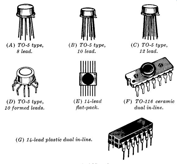
Fig. 7. Typical IC packages.
According to Packaging
Integrated circuits are sometimes described in terms of package type. In a few years, the number of IC types has grown tremendously, and these units are mounted in many different kinds of housings (more than 100 styles of case or envelope, at this writing). There are several common pack ages, however, and these are shown in Figs. 7 and 8.
The small TO-5 type cans (seen in Figs. 7 A, B, C, and D, and lower right in Fig. 8) resemble small-signal transistors and are of the same size. The somewhat larger TO-8 can also is used, as is also the TO-3 "power-transistor-type" package. The flat-pack type (Fig. 7E, and lower left in Fig. 8) resembles somewhat the old plastic-molded resistor capacitor networks. But the dual in-line packages (ceramic: Fig. 7F and upper right Fig. 8-plastic: Fig. 7G and upper left Fig. 8) are "new looks" in electronic components. All of these are tiny units.
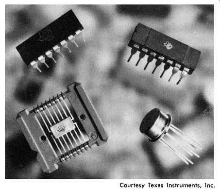
Fig. 8. Typical JC packages.
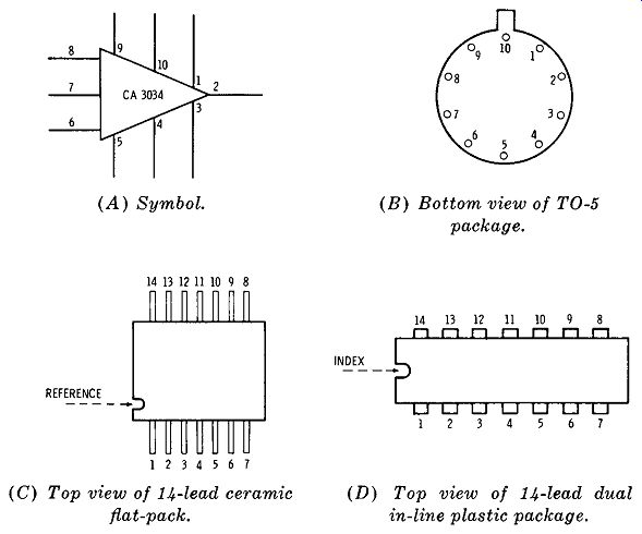
Fig. 9. Linear IC symbol and terminal layouts.
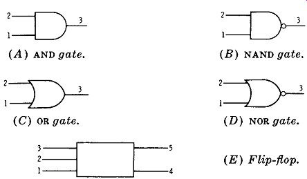
Fig. 10. Typical digital-IC symbols.
4. IC SYMBOLS
It would be tedious to draw most complete IC circuits (see, for example, Fig. 5), especially if several ICs are to appear in a schematic. The symbols shown in Fig. 9 and 10 represent complete ICs and greatly simplify draftsmanship.
The symbol for the linear IC is shown in Fig. 9; symbols for digital ICs are shown in Fig. 10. In each instance, the lines representing leads running to the IC terminals are numbered to agree with the actual terminal numbering of the IC. See, for example, the correspondence between the symbol (Fig. 9A) for the Type CA3034 IC and the pigtail numbering of this IC (Fig. 9B). It is not in every schematic that the numbering along the symbol follows the same sequence as the numbering of terminals on the actual IC; the sequence on the symbol is often a matter of drafting convenience. However, the terminals along the left vertical edge of the symbol (e.g., 6, 7, and 8 in Fig. 9A; 1 and 2 in Fig. 10A, B, C, and D; and 1, 2, and 3 in Fig. 10E) are usually input terminals, and the terminal (s) at the point of the symbol (e.g., 2 in Fig. 9A; 3 in Figs. 10A, B, C, and D; and 4 and 5 in Fig. 10E) are usually reserved for the output. (Sometimes, some other terminal near the right end of the symbol, along the top or bottom edge, may be the output.
For example, two such terminals, such as 1 and 3 in Fig. 19A may indicate the outputs of an IC having balanced or push-pull output. In Figs. 9A and B, correspondence is shown between the conventional triangular symbol and the numbering on the corresponding 10-lead TO-5 package. The numbering is not the same, however, on other packages.
Figs. 9C and D, for example, show the actual terminal numbering on ceramic flat-pack and in-line plastic packages, respectively. In the latter instance, where these 14 numbers are placed on the triangular symbol depends upon how the schematic is arranged (with the exception, of course, of the special places for input and output terminals, as explained above). Fig. 10 shows some common digital-IC symbols. Some reference was made to these in the preceding paragraph. In the gates (Figs. l0A to D), two inputs (terminals 1 and 2) and one output (terminal 3) are shown, but some gates have more than two inputs. In the flip-flop (Fig. l0E), three inputs (terminals 1, 2, and 3) and two outputs (terminals 4 and 5) are shown. Besides these input and output terminals, the digital IC, like the linear IC, has other terminals, but these have been omitted for simplicity in Fig. 10.
Some draftsmen use the triangular symbol (Fig. 9A) for all ICs, whether digital or linear. This simplifies matters, often considerably, and so long as the terminal numbering on the symbol corresponds to that on the IC package, no harm is done. In hobbyist-type schematics, the actual base diagram (Figs. 9B, C, D) often is used instead of the conventional symbol.
5. IC CHARACTERISTICS
Since most ICs are circuits, not single components, IC electrical characteristics are those of a circuit. In most instances, therefore, performance of the IC is specified not by some single parameter (such as f3 of a transistor or Gm of a vacuum tube), but by a series of parameters and ratings that describe operation of the particular integrated circuit.
An exception, of course, is the IC that consists only of two or more separate transistors or diodes; here, the usual transistor or diode characteristics are given.
The following list defines characteristics for which numerical data are found in the IC manufacturer's literature.
Amplification. See Gain.
Bandwidth. See Frequency Range.
Bias Current. Also called input bias current. The current into the IC input terminals in response to application of a signal voltage. Expressed in µA.
Common-Mode Gain. The voltage gain for common-mode input (see Fig. 12G).
Common-Mode Impedance. The input impedance (see Input Impedance) between either input of a differential amplifier IC (Fig. 12B to G) and ground. Expressed in ohms.
Common-Mode Rejection Ratio. The ratio of open-loop gain (Fig. 12F) to common-mode gain (Fig. 12G). Expressed in dB.
Differential-Input Impedance. The input impedance measured between the differential input terminals (INPUT 1 and INPUT 2 in Fig. 12F). Expressed in ohms.
Differential-Input Voltage Range. The range set by the maximum signal voltage that may be applied between differential input terminals (Fig. 12F) without over driving the IC amplifier.
Drift, Input-Voltage. The (usually slow) variation in output-signal voltage divided by the open-loop voltage gain of the IC. This drift is a function of time, temperature, and other factors. Expressed in m V /°C.
Frequency Range. The band of frequencies within which the IC will give specified performance. Expressed as DC to a specified high-frequency limit (e.g., DC to 50 MHz) or as the band width (e.g., 30 MHz).
Gain. The overall voltage gain of an amplifier-type IC. Fig. 12 shows the various modes of operation, with the corresponding voltage-gain formula given in each instance.
Note that in Fig. 12F, the input signal is applied between the INPUT 1 and INPUT 2 terminals, and the output is taken between the OUTPUT 1 and OUTPUT 2 terminals.
Note also that in Fig. 12G, the input signal is applied to the INPUT 1 and INPUT 2 terminals in parallel, and the output is taken between the OUTPUT 1 and OUTPUT 2 terminals. Expressed in dB. See also Common-Mode Gain and Open-Loop Voltage Gain.
Harmonic Distortion. In the output signal of an IC handling a sinusoidal signal, the ratio of total harmonic voltage to the fundamental-frequency voltage. Expressed in percent (along a 100% scale) at the test frequency.
Input Bias Current. See Bias Current.
Input Impedance. The impedance presented by the IC to the input signal. For ICs operated by a DC signal, this impedance is the input resistance. Expressed in ohms ( DC or at the specified test frequency) .
Input-Voltage Drift. See Drift, Input-Voltage.
Input-Voltage Offset. See Offset, Input-Voltage.
Noise Figure. The maximum intensity, or amplitude, of noise present in the output signal delivered by the IC. Expressed in dB.
Offset. The unbalance between the two halves of a symmetrical unit, such as the IC shown in Figs. 12B to G.
Offset, Input-Voltage. The value of DC input-signal voltage at the differential input (e.g., INPUT 1, INPUT 2, Fig. 12F) required to produce an output-signal voltage of zero. Expressed in mV.
Open-Loop Bandwidth. When an IC amplifier is operated without feedback, this is the band of frequencies within which the gain (see formulas in Fig. 12) is within 3 dB of a specified low-frequency value.
Open-Loop Voltage Gain. The gain of an IC amplifier operated without feedback. See also Gain and Fig. 12.
Output Impedance. The impedance "seen" at the output terminals of the IC. For ICs delivering a DC output signal, this is the output resistance. Expressed in ohms ( DC or at a specified test frequency) .
Output Swing. The maximum output-signal amplitude (with a given DC supply) which may be attained without IC over- load. Expressed in dcV or peak acV for a stated load resistance.
Power Dissipation. The maximum power which may be handled safely by the IC. Usually expressed in mW, but may be expressed in W for ICs containing a power output stage.
Power Output. The output-signal power delivered by an IC having a power output stage. Expressed in mW or W, at a specified load resistance.
Slew Rate. The maximum rate of change of the output signal of the IC, with respect to time. Usually expressed in volts per microsecond.
Supply Current. The DC operating current of the IC. For a single-supply IC (Fig. 11A), this is Irr• For a dual supply IC (Fig. 11B), this is Ice from the "collector-end" supply, and I •• from the "emitter-end" supply. Maximum and typical supply-current values are given in the IC manufacturer's literature. Expressed in mA or µA.
Supply Voltage. The DC voltage required to operate the IC. Some ICs may be operated from a single voltage source, V,.,., as in Fig. 11A; others require a dual supply Vrc and V •• , as in Fig. 11B. In the dual circuit, Ver is connected to the "collector end" of the IC, and v •• to the "emitter end." Maximum and typical supply-voltage values are given in the IC manufacturer's literature. Expressed in Vdc.
Temperature. The maximum temperature at which the IC may be operated safely. Expressed in °C.
6. INSTALLATION MECHANICS
ICs may be installed into larger circuits by the same means used for single transistors: (1) sockets, (2) contact clips or springs, (3) contact screws, and (4) direct soldering. In temporary experimental setups, flexible clip leads may be used.
Because of their small size and numerous contacts, ICs often require deft handling. A T0-5 unit (see Fig. 7C), for example, can have 12 flexible pigtails spaced around a circle less than ¼ inch in diameter ( considerably more crowding than that found in the 3-pigtail transistor) , and this arrangement demands patient handling to prevent bends and short circuits. The dual in-line packages (see Figs. 7F and G) have rigid lugs instead of pigtails, but 7 of these lugs are spaced along each edge of the housing in a line less than ¾ inch long.
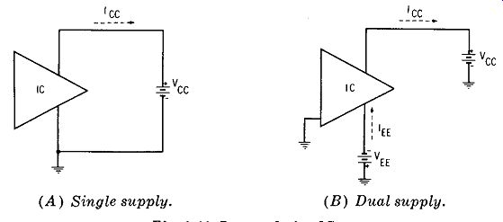
Fig. 11. DC supply for IC.
7. TYPICAL IC SETUPS
Most ICs offer considerable flexibility. Because of the numerous terminals at various parts of the internal circuit, the user may employ either the entire circuit or only those parts he needs, the unused portion of the IC simply idling or floating. This will be clear from an inspection of the operational-amplifier IC shown in Fig. 5. This entire IC may be used by applying an input signal to either INPUT terminal 3 or INPUT terminal 4, and taking the output signal from the single OUTPUT terminal 12. (A signal applied to 3 will appear amplified, but inverted in polarity, at 12, whereas the same signal applied instead to 4 will appear amplified and un-inverted at 12. That is, 3 positive = 12 minus, and 4 positive = 12 positive. The inverting input terminal (here, 3) sometimes is labeled negative, and the noninverting one (here, 4) positive. The entire IC thus offers two separate, identical-gain amplifiers, with a common, low-impedance (emitter-follower) output. And either amplifier can be placed into operation simply by applying DC voltages V cc and v •• and the input signal; no external components are needed.
Diodes X1 and X2; transistors Q5, Q6, and Q7; and resistors R3, R5, R6, R7, RS, and R1l form current sinks for stabilization of operation.
Sometimes, the entire circuit is not needed. For example, the input signal may be applied to 11, and only the output transistor ( Ql0) is used-as an emitter follower. Similarly, the input signal may be applied to 9, whereupon Q4 acts as a common-emitter amplifier direct coupled through Q8 to the emitter-follower output transistor, Q10. Also, a single input stage may be employed as a common-emitter amplifier by applying the input signal to 3 and taking the output signal from 1, or by applying the input to 4 and taking the output from 9. Other ways of going into this IC and coming out of it will suggest themselves to the reader.
The differential operational amplifier (abbreviated op amp) thus is one of the most useful linear ICs. The type of full-IC operation discussed above is illustrated by Fig. 13A. There being no overall feedback in this instance, the open loop voltage gain of the IC is realized. Open-loop operation is depicted also by all of the arrangements in Fig. 12.
But overall feedback may be used. This is illustrated by Figs. 13B to D. In Fig. 13B, external resistor R1 provides a feedback path from the output terminal to the inverting input terminal. The feedback therefore is negative. In Fig. 13C, external voltage divider R1-R2 divides the output signal voltage and applies the resulting voltage as feedback to the noninverting input terminal. This feedback therefore is positive. (When the positive-feedback amplitude is high enough, the opamp becomes an oscillator.) In Fig. 13D, both negative and positive feedback are obtained with external resistors R1 (negative), and R2 and R3 (positive). Opamps usually provide high gain. When the overall gain of a single IC is insufficient, however, two or more ICs may be cascaded, as shown in Fig. 13E. If required, feedback may be provided around each IC individually or around the entire cascade. In cascades, individual and combined phase shifts must be considered when feedback paths are planned.
In the two-IC cascade in Fig. 13E with IC1 and IC2 connected output-to-negative as shown, for example, a signal applied to the negative INPUT terminal, as shown, is un-inverted at the cascade OUTPUT terminal, whereas a signal applied to the positive INPUT is inverted at the cascade OUTPUT (both of these effects are the opposite of those obtained with a single IC). In a three-IC cascade, the phase relations of the single IC apply to the cascade. Thus, when identical ICs are employed and are connected together as shown in Fig. 13E, negative (inverting) and positive (non inverting) input labels must be interchanged in even numbered cascades, but may remain unaltered in odd-numbered cascades.
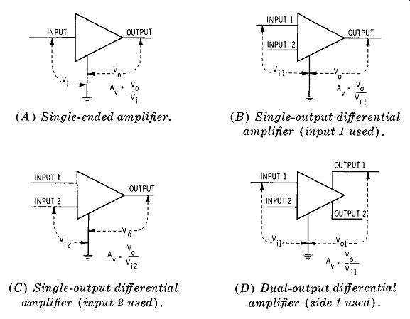

Fig. 12. IC amplifier input/output relationships. (A) Single-ended amplifier.
(B) Single-output differential amplifier ( input 1 used). ( C) Single-output
differential amplifier ( input 2 used). (D) Dual-output differential amplifier
(side 1 used). (E) Dual-output differential amplifier (side 2 used). (F) Differential
amplifier ( both sides used). ( G) Differential amplifier (common-mode input).
For simplicity, only resistors are shown in the feedback paths in Figs. 13B to D, and this sometimes is the case. Often, however, capacitors also are included-for isolation, RC tuning, etc. Similarly, coils, transformers, transistors, and other active and passive devices serve, where needed, as external ("outboard") components.
8. LARGE-SCALE INTEGRATION (LSI)
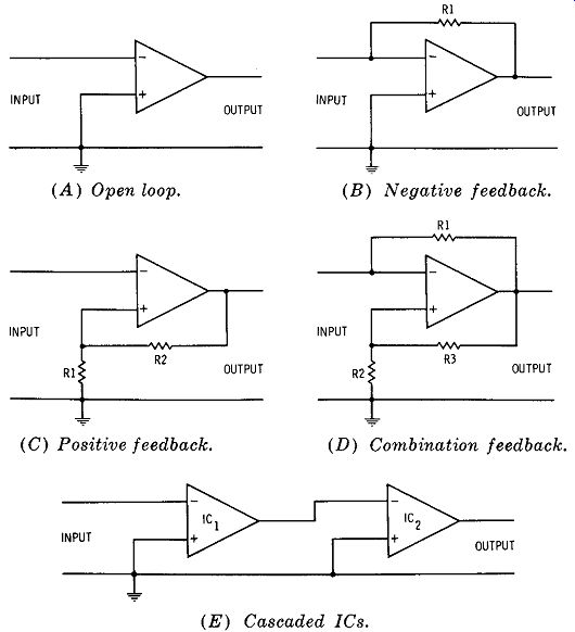
Fig. 13. Opamp operation. (A) Open loop. (B) Negative feedback. ( C) Positive
feedback. (D) Combination feedback. (E) Cascaded ICs.
Fig. 13E suggests that complicated systems may be built up comparatively easily by putting together the proper linear and/or digital ICs and adding any required external components. And this method is indeed employed in the DC sign and fabrication of a number of modern electronic systems.
The practice goes further, however, than simple implementations-the assembly of ICs and external discrete components into a larger circuit. A number of separate ICs and external components, together with all "wiring" may now be processed into a single wafer. This practice is referred to as large-scale integration (abbreviated LSI), and it will be increasingly responsible for dramatic size and weight reductions in all kinds of electronic equipment, especially computers, calculators, radar, and television.
A striking instance of size reduction through LSI is seen in the new mini-calculators that seem destined eventually to replace the engineer's slide rule. One model is smaller than a cigar box, weighs only 2.2 pounds, and performs the following operations: addition, subtraction, multiplication, division, chain multiplication and division, raising to a power, calculations by a constant, and mixed calculations.
Another example is a recently announced solid-state wrist watch. This regular-size timepiece contains more than 40 ICs--equivalent to about 3500 transistors.
9. TYPICAL IC APPLICATIONS
The following sections show typical applications of integrated circuits, in most instances single ICs. This presentation includes amplifiers (AF, dc, RF, video), oscillators, controls, receiver applications, transmitter applications, power-supply applications, test instruments, and analog computer applications.
The wide range of IC service is illustrated by this list, but the applications given here do not nearly exhaust the range of possibilities. The newcomer to ICs doubtless will be intrigued with the versatility and extended service of what appears to be a single component, the IC. In some instances, power-supply connections have been omitted for simplicity and clarity. If the reader wishes to duplicate these setups, he need only connect the DC supply to the IC terminals shown in the manufacturer's data. While specific IC's are shown in many instances and the values are given for outboard components, other schematics show only a class of operation and have no values. In the latter case, the user may adapt an IC he has to the indicated service.