Countless newcomers will have their first experience with the IC as a microminiature multistage amplifier. Indeed, many experimenters will already be accustomed to the "unit" amplifier in the form of a module, and they will regard the IC as nothing more than a tiny module. Some designers who must include an entire amplifier into other equipment will be intrigued with the convenience of the IC for this purpose.
In whichever category the user falls, he will appreciate the utility of the ready-made, miniature, IC amplifier. This section presents 15 representative applications of ICs in amplifiers of the following types: AF, dc, RF, i-f, and video.
Unless shown otherwise in the text or schematic, resistances are in ohms and capacitances are in microfarads, and electrolytic capacitors are rated at 50 Vdcw.
1. AMPLIFICATION POTENTIALITIES
As an amplifier, the IC offers a considerable range of possibilities. Depending upon model and configuration, the IC may provide operation from DC signals up to those at frequencies of several hundred MHz, voltage gain of more than 100 dB, single-ended or balanced output, voltage or power output, inverted and/or un-inverted output, and low DC power drain. In many instances, either the entire internal circuit or a portion of it may be used at will. In systems planning, the IC may be handled as a versatile black box having specified input and output characteristics.
While simultaneously providing voltage gain, with or without phase inversion, the IC may also function as a high to-low impedance converter. Additionally, the accessibility of various circuit points, via external terminals, enables the amplifier operation to be modified, as desired, through connection of external components and feedback networks.
In all amplifier applications, the IC thus saves the user a great deal of design effort and, at the same time, reduces the labor and time required for the assembly of amplifier systems.
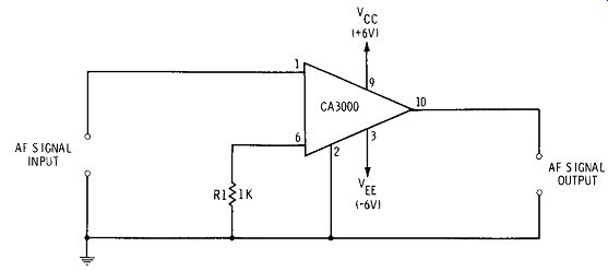
Fig. 1. Simplest AF amplifier.
2. SIMPLEST AF AMPLIFIER
The simplest possible IC audio-frequency amplifier is the IC itself with the minimum of external components. Fig. 1 shows such an arrangement. Here, a Type CA3000 unit is used with only one external 1k resistor (R1). The CA3000 contains two direct-coupled amplifier stages, each consisting of an input emitter follower plus an output common emitter. In the connection shown in Fig. 1, only one of these amplifiers is used; the other floats. The voltage gain of this connection is 30 dB. Without any external compensating components, the frequency response is DC to 1 MHz. Input impedance is 0.1 megohm, and output impedance is 8k. Both amplifiers may be used in cascade, with corresponding increase in gain, by connecting an interstage coupling capacitor externally between IC terminals 10 and 6 and taking the output from terminal 8, instead of terminal 10.
Gain control (by means of a potentiometer) and DC isolation of input and output circuits (by means of blocking capacitors) may readily be achieved, if required, through the connection of external components.
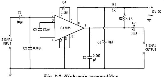
Fig. 2. High-gain preamplifier.
3. HIGH-GAIN PREAMPLIFIER
Fig. 2 shows the connections for a high-gain AF pre-amplifier employing a Type CA3035 IC. This circuit, DC signed by R. M. Marston, uses a single 12-volt DC supply.
The CA3035 contains three separate amplifiers, and all of them are used in cascade in the connection shown here. External capacitor C3 provides coupling between amplifier stages 1 and 2, and C4 provides coupling between stages 2 and 3. The voltage gain is 80 dB. The -3 dB bandwidth of the entire CA3035 is approximately 500 kHz.
If a gain-control potentiometer is employed, it must be connected at the output terminals or between amplifier stages ( e.g., at terminal 4 or 6), since the high gain of this IC (10,000) would cause potentiometer noise to be amplified if the gain control were installed at the input.
4. AUDIO DRIVER
The symmetrical output of the Type CA3007 IC is employed in Fig. 3 to drive the bases of a push-pull transistor, Class-B, AF, power-output stage (Q1-Q2). This circuit, due to RCA, requires two 6-volt DC supplies and as shown here is direct coupled to the Q1-Q2 stage, which can deliver 300 milliwatts output.
The CA3007 provides a typical power gain of 22 dB and has an input impedance of 4k ohms. A squelch voltage of +5 V presented to terminal 2 will cut off the amplifier.
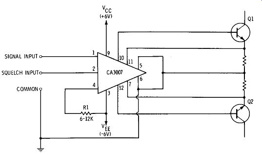
Fig. 3. Audio driver.
A driver of this type offers considerable simplification and size reduction, since the 12-lead TO-5 package of the CA3007 IC is smaller than the miniature coupling transformer alone required in most transistorized driver stages.
5. COMPLETE AF AMPLIFIER
Fig. 4 shows the connections for a complete AF amplifier delivering ½ watt to a loudspeaker. The Type CA3020 IC employed here contains input amplifier, phase inverter, and push-pull C1ass-B power-output stages, as well as a 3-diode type voltage regulator. Internally, direct coupling is employed between all stages. The IC is housed in a 12-lead TO 5 package.
Operated from a single 6- to 9-volt DC supply, this IC draws a zero-signal current of 7 mA and a maximum-signal current of 47 mA. The required input-signal amplitude is 35 mV. A heat sink is required.
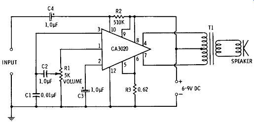
Fig. 4. Complete AF amplifier.
The required external components are four capacitors (C1 to C4), two 2-watt fixed resistors (R2, R3), one 5k volume control potentiometer (R1), and one miniature output trans former (T1: 125 ohms center tapped to 3.2 ohms). Two of these amplifiers, each no larger than a small-signal transistor and requiring only 9 external components including a loudspeaker, will supply the complete channels for a stereo phonograph.
Like other small-sized amplifiers having the same gain and power output, this amplifier is useful for purposes other than audio reproduction. It finds application, for example, in test equipment, alarm and signaling devices, modulators for low powered transmitters, etc.
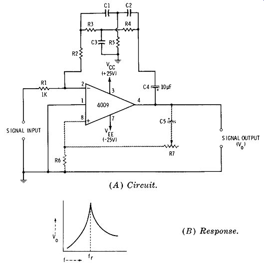
Fig. 5. Bandpass AF amplifier (RC type).
6. BANDPASS AF AMPLIFIER (RC TYPE)
External resistance-capacitance tuning is used in Fig. 2 5A to peak the frequency response of a high-gain AF amplifier. This is the familiar arrangement in which a twin-T null network (C1-C2-C3-R3-R4-R5) is connected in the negative feedback path of the amplifier. Fig. 5B shows the frequency response. A Type 4009 IC is used. Capacitor C4 provides DC blocking, and resistor R2 minimizes IC loading of the RC network, but neither of these components is a part of the tuned RC network.
In this arrangement, the negative feedback (back to inverting input terminal 2) ideally cancels the gain of the amplifier at all frequencies but the one that is nulled out by the twin-T network. The amplifier accordingly transmits this frequency (actually a narrow band of frequencies, as shown in Fig. 5B). The peak frequency fr is found from the formula:
where,
fr is in hertz, C1 is in farads, R3 is in ohms.
fr= 1/ (2 pi R3C1)
Also, C1= C2 = ½ C3, and R3 = R4 = 2R5.
The response may be sharpened by providing positive feedback (back to non inverting input terminal 8) through the adjustable signal divider, R6-R7. Sharpest peaking occurs when the positive feedback is set just below the point at which the amplifier oscillates. The amplifier tuning may be made continuously variable (say, from 20 Hz to 20 kHz) by using a 3-gang tuning potentiometer for R3-R4-R5, and switching C1, C2, and C3 in trios to change bands.
The obvious advantage of this type of tuned amplifier is its ability to operate without bulky iron-core inductors, and to provide tuning at low audio frequencies. However, two difficulties have always accompanied actualization of the circuit. One is the need that the amplifier have sufficient gain to overcome the losses of the feedback network. The other is that the gain of the basic amplifier be constant over a wide frequency range if the tuned amplifier is to be used throughout the audio spectrum. The IC overcomes both of these difficulties, providing high gain ( through cascaded internal stages) and wideband operation (through direct interstage coupling) .
7. BANDPASS AF AMPLIFIER (LC TYPE)
Although the bandpass amplifier described in preceding Section 2.6 is divorced from all inductors, there are instances in which sharper response is needed than that afforded by RC tuning. The higher Q available with inductor-capacitor tuning provides the narrower passband that is required.
Fig. 6A shows essentially the same circuit with an inductor-capacitor null circuit (L1-C1) in the negative feedback path. The corresponding frequency response is illustrated by Fig. 6B. The mode of operation of this tuned amplifier (employing a Type 4009 IC) is the same as that explained in the preceding section, except that L1 and C1 (instead of a twin-T RC network), acting as a wavetrap, remove the feedback frequency to which this combination is resonant; accordingly, this frequency is the one that the amplifier transmits. The resonant frequency fr is found by the formula: where, fr is in hertz, L1 is in henrys, C1 is in farads.
fr= 1/ (2 pi L1C1)
Also, from the preceding formula, C1 = 1/ ( 4 pi 2 f2 L1), and L1 = 1/ (4 pi 2 f^2 C1). As in the preceding amplifier, the response may be sharpened still further by means of positive feedback obtained through the R3-R4 signal divider and adjusted just short of the point of oscillation.
The LC-type bandpass amplifier has the obvious disadvantage that it cannot easily be continuously tuned, since L1 and C1 ordinarily are too large to be made continuously variable. However, a small amount of tuning is possible by employing one of the adjustable-core (screwdriver-tuned), high-Q inductors that are commercially available.
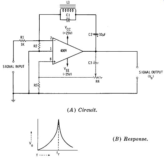
Fig. 6. Bandpass AF amplifier (LC type).
8. BANDSTOP AF AMPLIFIER (RC TYPE)
Fig. 7 A shows the connections for a band-stop amplifier employing a Type CA3035 IC. Ideally, this amplifier removes one frequency (actually a narrow band of frequencies, as shown in Fig. 7B), transmitting all other frequencies with little attenuation.
The frequency that is nulled out is determined by the resistance and capacitance values in a twin-T RC network
(R1-R2-R3-C3-C4-C5) connected between amplifier stages 1 and 2 of the IC. The null frequency fr is found by the formula: where, fr is in hertz, R1 is in ohms, C3 is in farads.
fr= 1/ (2 pi R1 C3)
Also, C3 = C4 = ½ C5, and R1 = R2 = 2R3.
As in the bandpass amplifier described in Section 2.6, the tuning may be made continuously variable ( e.g., from 20 Hz to 20 kHz) by using a 3-gang tuning potentiometer for R1 R2-R3, and switching C3, C4, and C5 in trios to change bands.
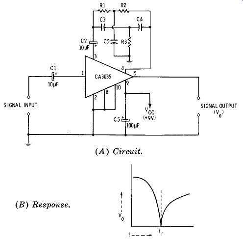
Fig. 7. Bandstop AF amplifier (RC type).
9. BANDSTOP AF AMPLIFIER (LC TYPE)
Although the bandstop amplifier described in preceding Section 2.8 offers the advantage of operation without inductors, there are instances in which sharper tuning and a deeper null are needed than are obtainable with RC tuning.
The higher Q obtainable with inductor-capacitor tuning provides the narrower passband required under such circum stances.
Fig. 8A shows essentially the same circuit with an inductor-capacitor null circuit (L1-C1) connected between amplifier stages 1 and 2 of the Type CA3035 IC. The corresponding frequency response is illustrated by Fig. 8B. The mode of operation of this amplifier is the same as that explained in Section 2.8, except that here L1 and C1 (instead of a twin-T RC network), acting as a wavetrap, remove the frequency to which this combination is resonant. The null frequency fr is found by the formula: where, fr is in hertz, L1 is in henrys, C1 is in farads.
fr= 1/ (2 pi __/L1C1)
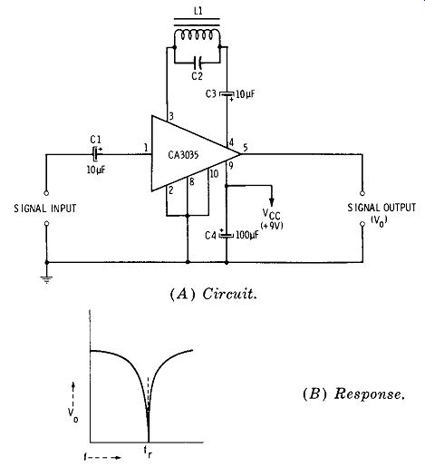
Fig. 8. Bandstop AF amplifier (LC type).
Also, C1= 1/(4 pi^2 f^2 L1 ), and L1 = 1/(4 pi^2^f^2 C1 ). The 10-µF capacitor, C3, serves only for DC blocking and does not enter into the frequency determination.
The LC-type bandstop amplifier has the obvious disadvantage that it cannot easily be continuously tuned, since L1 and C1 ordinarily are too large to be made continuously variable. However, a small amount of tuning is possible by employing one of the adjustable-core (screwdriver-tuned), high-Q inductors that are commercially available.
10. CASCADED-IC AF AMPLIFIERS
Although ultrahigh-gain ICs are available, there are AF applications demanding higher gain than that afforded by a single IC. For higher gain, ICs may be cascaded (see Fig. 13E and Section 1.7, Section 1). In general, recommended practices for cascading ICs are the same as those for cascading other types of npn transistor amplifiers. Important considerations, for example, are (1) noise amplification, (2) cumulative drift effects, (3) overdriving, (4) decoupling requirements, and (4) overall phase shift.
Cascading of high-gain ICs is common practice where extremely high sensitivity is desired. In most instances, how ever, available lower-gain ICs will be cascaded in order to approximate the capabilities of an ultrahigh-gain IC that is not immediately available.
11. STEREO PREAMPLIFIER
Fig. 9 shows the connections for a 2-channel preamplifier for stereo phonographs. This circuit is RIAA equalized and is a design by Fairchild Semiconductors. For the two channels, the two halves of a µ,A 739C IC are used (two separate IC symbols are shown, as this reduces crowding in the schematic, but all of the terminals could have been shown on one triangle). Each channel provides a voltage gain of 40 dB at 1 kHz.
The RIAA-equalized input overload point is 80 m V rms.
The signal-to-noise ratio is 74 dB below 10 mV, and the channel separation is 80 dB at 1 kHz.
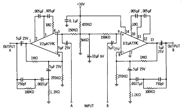
Fig. 9. Stereo preamplifier.
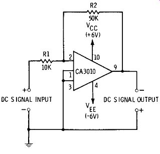
Fig. 10. De voltage amplifier.
12. DC VOLTAGE AMPLIFIER
Because of its direct coupling and stability, the operational-amplifier IC works well with DC signals. Fig. 10 shows the connections for a DC voltage amplifier employing a Type CA3010 IC. This arrangement has an input resistance in excess of 15k and an output resistance of 200 ohms.
Operated from a dual DC supply (Vee= +6 V; V •• = -6 V), this arrangement has a voltage gain of 4, for a maximum DC input signal of 1 volt. Negative feedback is provided by the 50k resistor, R2, connected from output terminal 9 to inverting input terminal 2.
DC amplifier ICs may be cascaded, provided the precautions necessary in the cascading of any direct-coupled transistor amplifiers are heeded. It is necessary also in the case of cascaded IC DC amplifiers to take into account the effects of individual offset and slew in the entire setup, and to compensate for these when they are significant.
13. RF AMPLIFIER
Fig. 11 shows the connections for a tuned radio-frequency amplifier based upon a Type CA3005 IC. This circuit is adapted from the original RCA version. If the amplifier is used for standard broadcast-band service, T1 may be a ferrite loopstick antenna of the two-coil variety, and T2 will be a matching tRF "coil." The CA3005 contains two amplifiers (a differential arrangement) and a stabilizing circuit. This unit has a useful frequency range of DC to 120 MHz and is housed in a 12-lead TO-5 package. It can provide a power gain of 16 dB in the differential arrangement shown in Fig. 11.
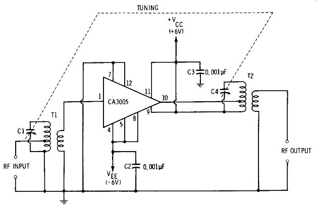
Fig. 11. RF amplifier.
14. IC AS UNTUNED RF AMPLIFIER
In applications in which selectivity is not demanded, a wideband IC amplifier may be used as an untuned RF amplifier. For applications of this type, many ICs have suitable frequency specifications. The following are a few examples: CA3000 (dc-30 MHz), CA3001 (dc-20 MHz), CA3004 (de-120 MHz), CA3005 (dc-120 MHz), CA3013 (100 kHz-20 MHz), CA3020 (dc-8 MHz), CA3021 (dc-6 MHz), CA3023 (dc-40 MHz), CA3028 (dc-120 MHz), CA3034 (dc-100 MHz), and 4009 (dc-30 MHz). A common use of an untuned RF amplifier is the aperiodic preamplifier or booster found in some test instruments and radio receivers. The numerous well-known precautions that ordinarily are important in the construction and use of such amplifiers must be observed also when ICs are used.
15. IF AMPLIFIER
Fig. 12 shows the connections for a single intermediate frequency amplifier stage based upon an RCA design for the CA3012 IC. The frequency response of this IC extends from 0.1 MHz to more than 20 MHz, and the single-battery arrangement shown in Fig. 12 is effective at the 10.7-MHz fm intermediate frequency.
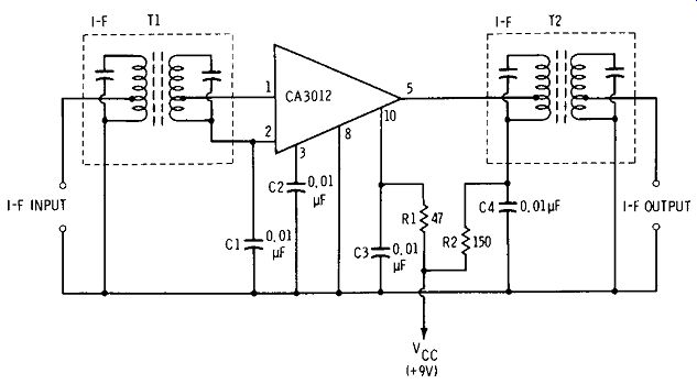
Fig. 12. IF amplifier.
The tapped transformers allow improved impedance matching at the input and the output of the IC. The IC manufacturer shows a voltage gain of 65 dB between terminals 1 and 5 of the IC in this i-f amplifier circuit (based upon a 3.5-µ, v signal at terminal 1) . Two such stages usually are employed in a superhet receiver. Transformer-coupled stages of this type usually can be cascaded without difficulty.
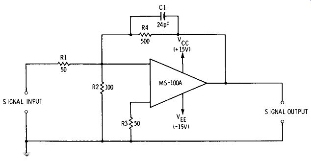
Fig. 13. Video amplifier (1).
16. VIDEO AMPLIFIERS
The extended bandwidth of many linear ICs suits these units for video amplifier service. Fig. 13 shows the connections for a video power amplifier, due to Sylvania. Employing an MS-l00A IC, this amplifier works between a 50-ohm source and a 50-ohm load. (The output impedance of the MS-l00A itself is less than 2 ohms.) The voltage gain is 10 dB, and the 3-dB bandpass is DC to 18 MHz.
A second video amplifier, shown in Fig. 14, is based upon the CA3001 video-amplifier IC and follows the original RCA design. Driven by a 50-ohm source, this amplifier provides voltage gain in excess of 15 dB from DC to 5 MHz. At approximately 18 MHz, the gain is 3 dB down from that figure.
Typical input resistance of the CA3001 is 50 ohms, and out put resistance is 70 ohms.
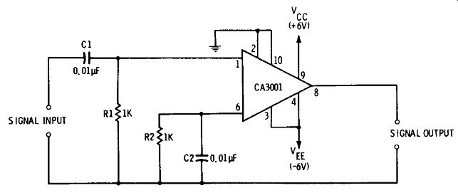
Fig. 14. Video amplifier (2).