| PREV: SOLID-STATE DEVICES USED FOR LOGIC | NEXT: SOLID-STATE LOGIC BLOCKS |
Solid-state devices such as transistors can be arranged in circuits to provide AND and OR functions like the relay circuits. (See in ill. 1 below.) From this example, notice that inputs of the AND and the OR transistor circuits are identified as input 1, input 2, and input 3. The output of the AND circuit is identified as output 1, and the output of the OR circuit is identified as output 2.
AMAZON multi-meters discounts AMAZON oscilloscope discounts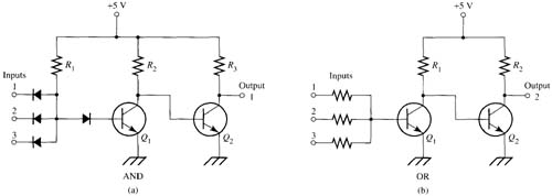
Above: ill. 1: Transistor circuits for
the AND logic function and the OR logic function.
Each part of the transistor logic circuit has an equivalent function in the relay logic. In the transistor logic circuits, applying +5 volts is the equivalent of the closed switch in the relay logic circuit. The +5 volts signal is also called a high, HI, or true signal. If the input to the circuit is grounded or pulled to 0 volts, it's equivalent to having open contacts in the relay circuit. The grounded input or 0 volts is called a low, LO, or false signal. When the coil in the relay logic circuit is energized, it becomes magnetic and pulls in its contacts. The transistor logic circuit provides a logic HI signal (+5 volts) at the output line of the circuit when the circuit becomes true.
Notice in the transistor AND logic circuit in ill. 1 that three inputs are available just as in the AND relay logic circuit. To fully understand the circuit operation when a HI signal is present at each input, you must first understand when a LO signal is present.
Notice that a diode is connected in the input part of each circuit. If the input is grounded, the diode will be forward biased and current will flow from the circuit supply through the limiting resistor through the diode to ground. You should remember that when a diode is forward biased, its anode voltage will be approximately 0.6 volts. This will be considered a LO signal. When this occurs at any one of the three inputs, only 0.6 volts will be available at the anode of the diode D2 in the base of transistor Q which won't be sufficient to bias it. That is, VCE will be maximum and the transistor is effectively an open circuit. Since transistor Q is open, sufficient voltage will be supplied to the base of Q2 through resistor R The base voltage at Q2 will be sufficient to cause it to saturate so its collector will be effectively the same potential as ground, which means output 1 terminal will be LO. If any one of the inputs to Q are supplied with a LO signal, the output of the circuit at Q2 will also be LO.
When all of the inputs to Q1 are supplied a HI signal, sufficient base current will be supplied to Q1 and it will saturate. This will cause the base of Q2 to become grounded, which will cause its collector-emitter circuit to go to cutoff. That is, voltage from the +5 volts supply will be present at the output, which indicates the circuit has a HI signal. That is, input 1, AND input 2, AND input 3 must all be HI to have a HI output for the logic circuit.
The transistor circuit for the OR logic is similar to the AND logic circuit in that three inputs are provided and two transistors are used. When any one of the input circuits go HI, transistor Q1 will become saturated, which causes the collector to become grounded. When the collector of Q becomes grounded, the base of Q2 is also grounded. This causes Q2 to go to cutoff, which means that the +5 volts supply voltage will be available at the output terminal. The only time the output of the OR circuit is low is when none of the inputs are HI.
| Top of Page | PREV: SOLID-STATE DEVICES USED FOR LOGIC | NEXT: SOLID-STATE LOGIC BLOCKS |