AMAZON multi-meters discounts AMAZON oscilloscope discounts
Contents:
INTRODUCTION
RF POWER AMPLIFIER FUNDAMENTALS
Current and Voltage Relationships
Tank Circuits
Coupling Methods
VACUUM TUBE RF POWER AMPLIFIERS
Bias Methods
Amplifier Stability
Multielement Tube Stages
Multitube Stages
Frequency Multipliers
TRANSISTOR POWER AMPLIFIERS
Biasing Methods
Multi-transistor Amplifiers
Frequency Multipliers
Amplifier Stability
ADJUSTING CLASS C AMPLIFIERS
The Vacuum Tube Stage
The Transistor Stage
LESSON QUESTIONS
++++++++++++++
Introduction
A radio transmitter is a device for converting some form of intelligence into electrical impulses suitable for transmission through space. In its simplest form, a transmitter consists of a source of rf energy, called the master oscillator, and one or more stages of rf power amplification.
In practical transmitters, such as the one shown in block diagram form in Fig.1, there are a number of stages between the master oscillator and the antenna. Since each stage is a form of rf power amplifier, let's briefly discuss the particular role each one plays in the overall operation of the transmitter.
Immediately following the master oscillator is a stage called the buffer amplifier. Its purpose is to present a light, constant load to the oscillator, which helps maintain a stable oscillator frequency.
The FCC requires that very close control of output frequency be maintained on all radio transmitters under its jurisdiction.
The next stage, called a frequency multiplier, produces an output whose frequency is some multiple of the input frequency. The presence of this stage permits the master oscillator to be operated at a frequency lower than the transmitted frequency. It is much easier to design highly stable oscillator circuits at the lower radio frequencies; therefore, one or more frequency multiplier stages are an essential part of most radio transmitters.
The driver and power output stages provide the remaining amplification necessary to supply power to the antenna. This output power may range from less than 100 watts to 1 million watts, depending on the transmitter type and the purpose for which it is to be used. In recent years low power circuits, which formerly used vacuum tubes, have been redesigned to use economical, efficient transistors.
In many low to medium power mobile transmitters, transistors are used in all stages delivering as much as 75 watts of rf output power at 175 MHz. In other transmitters, all but the driver and final amplifier (power output) stages have been replaced by transistors. There is every reason to suppose that this trend will continue as the high-frequency power handling capability of transistors is improved.
The vacuum tube, however, is still used in high power stages of transmitters which are employed in the AM, TV, and FM broadcast fields. It will no doubt remain so for quite some time to come.
Very large vacuum tubes are required to handle the enormous power outputs of these transmitters.
There are three characteristics of all rf power amplifiers, transistors, or vacuum tubes which are of concern to us. They are linearity, power gain, and efficiency.
The linearity of an amplifier is a measure of how closely the amplified output follows the input; in other words, a measure of how much distortion is introduced into the output signal by the amplifier. Linear amplifiers, which introduce very little distortion into the signals they amplify, are a subject in themselves and will be considered in a later lesson.
Figure 1. Block diagram of a basic transmitter. All the stages are operated
class C.
The power gain of an amplifier, usually expressed in db, tells us how much the power level of the input signal is increased by the amplifier. Power gain depends on circuit design and the tube or transistor type used in the circuit. Beam power tetrodes have the highest power gain of any other conventional vacuum tube type. For this, as well as other reasons, the beam power tetrode is the most commonly used tube in modern transmitters. The power gain of transistors does not compare favor ably with that of vacuum tubes at higher radio frequencies. This limitation may be partially over come by adding more stages or using more than one transistor in each stage.
The efficiency of an amplifier, expressed as a percentage, is the amount of dc input power to the stage actually converted to rf energy at the output.
In a vacuum tube stage, the power input is the product of the plate supply voltage times the average current. For example, suppose the plate supply voltage is 3000 volts, the plate current 450 milliamps, and the power output of the stage 1000 watts. The dc input power to the stage is:
P=E X I = 3000 X 0.45 = 1350 watts
The efficiency of the stage can then be found by using the following formula:
Power Out % Efficiency - X 100
Power In 1000 X 100 = 74% 1350
In a previous lesson, you learned that class C amplifiers give the highest practical efficiency, ranging up to 75%. This is compared to efficiencies of 35% to 50% for class B and as little as 30% to 35% for class A. However, the high efficiency of class C amplifiers is obtained at the expense of linearity. As you'll remember, output current flows for less than half the input cycle in a class C amplifier. This output current pulse bears little resemblance to the input signal which produced it and is therefore highly distorted.
If the output circuit of the class C amplifier is a resonant tank, this current pulse shock-excites the tank so that a complete sine wave is produced.
Thus the nonlinearity of the class C amplifier is effectively eliminated when a single rf frequency (a sine wave) is to be amplified. This, along with the class C amplifier's high efficiency, makes it suitable for many rf power amplifier applications.
In the next section we'll discuss class C rf amplifier fundamentals. The information presented in this section applies to both vacuum tubes and transistors. Later, we'll discuss specific applications of vacuum tube and transistor amplifiers. In the final section, we'll talk about the various adjustments which may be made to both types of amplifier circuits.
RF Power Amplifier Fundamentals
In any amplifier, heat is generated by the current flow through the internal resistance of the stage. The power used to generate this heat represents wasted energy and subtracts from the power that could go to the output. The high efficiency of a class C amplifier is due largely to the fact that current flows for a relatively short portion of the input cycle. It is only during this short conducting period that power-wasting heat is generated within the amplifier. To begin our discussion of class C amplifiers, we'll consider the relationships between the current conducting time and the signal voltage waveforms in an operating class C amplifier.
Figure 2. Output current pulse produced by input signals at various amplitudes
and bias levels.
CURRENT AND VOLTAGE RELATIONSHIPS
The graph in Fig.2 shows the output current pulse produced by an input signal at various dc bias levels. Look first at the signal at bias level 1. This signal is below the cutoff value of the amplifier for all of the negative half-cycle and nearly all of the positive half-cycle. Output current flows only for the time the input voltage goes above cutoff. Now look at the signal at bias level 2. It has the same amplitude as the first signal but, because we've increased the bias, this signal exceeds the cutoff level for a shorter period. As a result, the output current pulse produced also flows for a shorter period and is lower in amplitude. Increasing the amplitude of the input voltage has the same effect as decreasing the bias. That is, the output current flows for a longer time.
Another way of looking at these basic relation ships is shown in Fig.3. Figure 3(A) shows two basic class C amplifiers; one uses a vacuum tube, the other a transistor. Figure 3(B) shows the voltage and current waveforms appearing at the inputs and outputs of the amplifiers. Again notice that output current flows only during the period when the input signal exceeds the cutoff level of the amplifier. The output voltage waveform E Out is produced by the flywheel action of the resonant output circuit.
Figure 3. Basic relationships between current and signal voltages in a
class C amplifier.
Conduction Angle. There are 360 electrical degrees in one complete cycle of a sine wave. The number of electrical degrees the output current flows in a class C amplifier is called the conduction angle or operating angle of the stage. As you've seen, the operating angle depends on both the dc bias and the amplitude of the driving signal.
Although amplifier efficiency is higher at the smaller operating angles, the power output is less because the output current pulse is reduced in amplitude and flows for a shorter period. There fore, the operating angle must be a compromise between maximum efficiency and the highest power output. In making this compromise, the driving signal is maintained at a level sufficient to drive the stage into saturation while the bias is adjusted for the correct operating angle.
Driving Power. To drive a vacuum tube amplifier into saturation requires that the grid be driven positive. The positive grid draws current, causing power to be consumed in the grid circuit. Likewise, in a transistor amplifier, base current flows during the time the driving signal forward-biases the emitter-base junction. The result of this base current flow is that power is consumed in the base circuit.
The power consumed in the input circuit of a class C amplifier, called the driving power, must be supplied by the previous stage. Thus the input circuit of one class C amplifier represents the load on the stage which comes before it. Furthermore, this load presented by the input circuit varies over the period of an operating cycle, reaching a maximum when the input signal causes maximum current to be drawn. As we'll see later, we can use this current flow in the input circuit to develop bias for the stage.
TANK CIRCUITS
The resonant circuit in the output of a class C amplifier has several important jobs to do. We've already mentioned the most basic of these, that of changing the output current pulse into a complete sine wave. This resonant circuit is also required to present the proper load impedance to the stage, and to suppress the undesired harmonics generated within the stage. Let's discuss these last two in detail.
Load Impedance. In order to obtain the maximum power gain from a class C amplifier, or any other amplifier for that matter, the impedance of the load must match the internal impedance of the amplifier. However, do not confuse power gain with power output. It is quite possible that an amplifier operating with a matched load, for maximum power gain, is not delivering its maxi mum output power.
This is especially true for transistor rf power amplifiers. These amplifiers are very often designed to operate from automotive type battery supplies, thus limiting collector supply voltages to the 12 to 28 volt range. With the load matched to the internal impedance of the amplifier, there may be insufficient collector current flow to give the required power output. Using a value of load resistance lower than the input impedance of the stage results in a greater collector current flow and higher power output. Therefore, in some cases power gain must be sacrificed for power output.
Factors Affecting Impedance. Since the output tank circuit must offer the correct load impedance for the class C amplifier, let's look at some of the factors which affect this impedance. We know that to be resonant, the L and the C of the tank circuit must offer equal reactances at the operating frequency. If we increase the value of L, the value of XL will increase. To maintain resonance, we must increase Xc by decreasing C. Having in creased the value of XL and Xc by equal amounts, we have increased the total impedance of the circuit without affecting the resonant frequency.
Any resistance present in the tank acts to decrease the total impedance of the circuit. The values of C, L, and R are related to total impedance by the following formula: From the formula, you can see that increasing the ratio of L to C in the tank causes the impedance to increase. Increasing the resistance in the tank causes impedance to decrease. This leads us to a discussion of tank circuit Q. Circuit Q. The Q of a coil, as you know, is the ratio of its reactance to its resistance or: Q = XI
A capacitor also has a Q, but its value is very large due to the capacitor's low internal resistance. The Q of a tank circuit, therefore, is equal to the Q of the coil.
Figure 4. Amplifier with a parallel-tuned output tank showing impedances
at resonance.
Figure 4 shows an amplifier with a parallel tuned tank circuit in its output. At the operating frequency of this amplifier, let's assume the XL of the coil is 6000 ohms and its resistance (Rs) is 20 ohms. The Q of this unloaded tank circuit then is:
XL 6000 Q = - = 300 Rs 20
The Q of unloaded tank circuits in practical transmitters may range from 200 to 800. Figure 5(A) shows the same amplifier of Fig.4 inductively coupled to a load. This load might be a trans mission line, an antenna, or another rf amplifier.
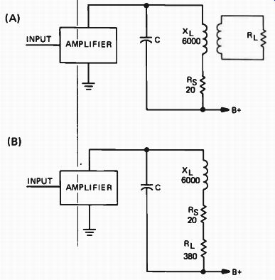
Figure 5. Tank circuit coupled to a load and its equivalent circuit.
The effect of this load is to reflect an additional resistance into the tank circuit. The equivalent circuit, shown in Fig.5(B), contains this reflected resistance ( RL') in series with the resistance of the coil. The exact value of RL' depends on the value of the load resistance as well as the coupling to the load. We'll assume a value of 380 ohms for our discussion. The Q of the tank now becomes:
XL 6000 15 Q = - RL' + Rs 400 -
Thus, the Q of the tank circuit went from an unloaded value of 300 to the loaded value of 15 due to the resistance reflected into the tank circuit by the load. From the previous discussion of tank impedance, you know that this additional resistance in the tank also decreases the impedance of the tank. Tank Q and tank impedance are closely related quantities. Factors which change one will also change the other in the same direction.
Let's see now why this is important. You know that only the resistance in a circuit consumes power. Inductive and capacitive reactances, under conditions of resonance, merely transfer energy back and forth between themselves. Therefore, when the tank is loaded, all of the power in the circuit is consumed by the resistances Rs and RL'. The power consumed in RL' represents power consumed by the load, while that consumed by Rs is dissipated as heat in the tank circuit. From Ohm's law we derive that P = PR, so the power consumed by the load far exceeds that lost as heat in the tank. This is because of a larger value of RL'. We can actually calculate the efficiency of the tank circuit by the formula:
% Efficiency = (1 Q L ) Qu X 100
In our example, the unloaded Q (Qu ) was 300, and the loaded Q ( QL) was 15.
Therefore:
15 ) %
Efficiency = (1 300 X 100 = (1 - 0.05) X 100 = 95%
Suppose we increased the coupling to the load and reflected a larger value of resistance into the tank. This would decrease QL without affecting Qu , resulting in a higher tank circuit efficiency.
But remember, tank impedance is dependent on the resistance in the tank, so changing the coupling to the load changes the tank impedance. Since the stage is designed for best operation at a particular tank impedance, there is only one correct value of loading on the tank.
Reducing Harmonics. The output pulse of a class C amplifier contains, in addition to the fundamental, numerous harmonic frequency components. As you'll learn later in this lesson, this fact enables us to operate a class C stage as a frequency multiplier. The output tank circuit offers maximum impedance at the frequency to which it is tuned. Harmonic frequencies, seeing a relatively lower impedance, are not developed across the tank circuit in any great magnitude. The circuit which couples the tank to its load is usually designed with harmonic suppression in mind.
Sometimes, special traps must be used in output coupling networks which either shunt the harmonics to ground or block their passage to the antenna.
An additional precaution against harmonic radiation is to use an electrostatic shield between two inductively coupled circuits. A shield of this type, called a Faraday screen, is shown in Fig.6.
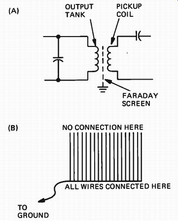
Figure 6. An electrostatic shield or Faraday screen between the output
tank and the antenna pickup coil is used to prevent harmonic currents from
flowing through the capacity between the coils.
The Faraday screen consists of a number of wires fastened together at one end and open at the other. The ends of the wires that are connected together are grounded. Capacitively coupled harmonic currents will flow to the screen wires rather than to the pickup coil. At the same time, because the wires do not form closed circuits, there can be no voltage induced in them by the magnetic field.
Therefore, they do not interfere with the inductive coupling between the output tank and the link coil. This method is very effective in reducing the transmission of harmonics from an output tank circuit to an antenna or transmission line.
COUPLING METHODS
The resonant tank in the output of a class C amplifier forms the basis of the coupling circuit to the amplifier's load. We know that the impedance presented to the stage by the output tank circuit depends, to a large measure, on the equivalent resistance in the tank. We also know that the value of this equivalent resistance is primarily that reflected into the tank by the load. To obtain the correct tank impedance for the amplifier, the coupling must reflect a certain value of resistance into the tank. In most cases, the actual value of the load resistance connected directly across the tank would not reflect the correct resistance into the tank. Therefore, the coupling method must give an impedance transformation. The simplest way to accomplish this impedance transformation is to use a transformer as a method of inductive coupling.
Inductive Coupling. Figure 7 shows two amplifier stages inductively coupled together. In this circuit, the resistance reflected into the output tank for amplifier 1 is adjusted by varying the spacing between the coils. Varying this spacing also adjusts the drive to amplifier 2. The circuit is designed to reflect the correct resistance and provide the proper drive at the same setting.
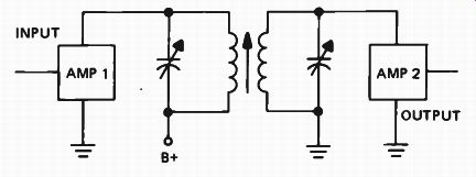
Figure 7. Inductively coupled amplifiers.
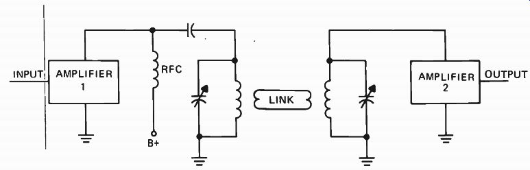
Figure 8. Link coupled amplifiers.
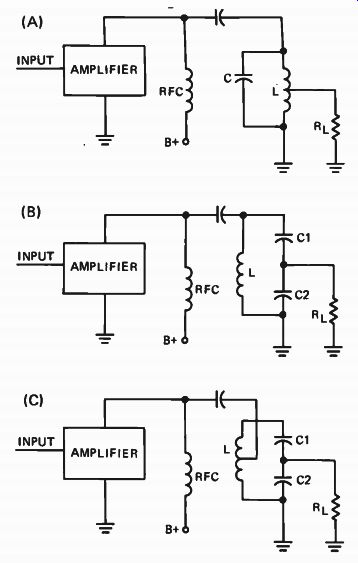
Figure 9. Tapped tank circuits used for impedance transformation.
A variation of inductive coupling is shown in Fig.8. This method is called link coupling. It consists of a coil with only a few turns of wire inductively coupled to an output tank. A similar coil is inductively coupled to the load. The connection between the two coils is usually by means of shielded coaxial cable, so it may run some distance with very little loss. Link coupling may also be used between the final power amplifier in a transmitter and a low impedance transmission line. As in the conventional inductive coupling already discussed, the coupling is adjusted by varying the spacing between one of the link coils and the tank. Sometimes the link itself is tuned by a variable reactance. When this is done, the tuned link provides additional suppression of harmonics generated in the previous stages.
Notice that the method of applying B+ to the stage in Fig.8 differs from that of Fig.7. In Fig.8, this voltage is applied through a radio frequency choke (rfc). The rfc offers a very high impedance at the operating frequency, so it keeps the signal voltage out of the power supply. When the power supply, the tank circuit, and the stage are connected in series, as in Fig.7, the amplifier is said to be series-fed. When the power supply, tank circuit, and stage are in parallel (or shunt), as in Fig.8, the amplifier is said to be shunt-fed.
Tapped Tank Circuits. Another method of obtaining an impedance transformation is to connect the load across only a portion of the tank coil.
Such a method is shown in Fig.9(A). The value of resistance reflected into the tank is dependent on the position of the tap. In Fig.9(B), the tank capacitor is split to provide the impedance trans formation. The values of C1 and C2 determine the value of load resistance seen by the tank (reflected resistance).
The methods shown in Fig. 9(A) and 9(B) may be combined as shown in Fig.9(C). With this circuit arrangement, the internal impedance of the stage, as seen by the tank, is transformed to a higher value by the tapped coil. Using this method the required value of loaded Q in the tank may be maintained in spite of low values of internal impedance (such as found in transistor stages). The values of C1 and C2, as before, determine the value of load resistance seen by the tank.
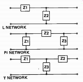
Figure 10. Networks used to couple an amplifier to its load.
Network Coupling. Figure 10 shows three types of networks frequently used to couple class C amplifiers to their loads. The various arms of each are shown as impedances in the figure. In practical networks of this type these impedances will be combinations of L and C components.
Later on in your course you'll learn to calculate the reactance values for the arms of these networks to give a required impedance transformation. For now, it is enough for you to know that they fulfill all the requirements of a tank circuit and can provide impedance transformations over a very wide range of values. In addition, these circuits can be easily designed to attenuate undesired harmonic frequencies.
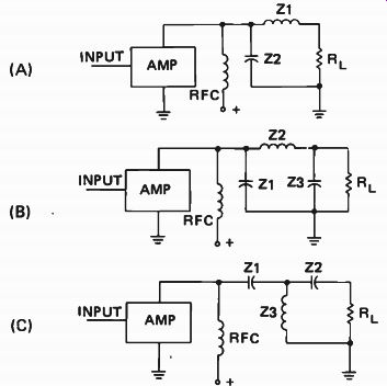
Figure 11. Amplifiers using L, 77, and T network coupling to load.
Figure 11 shows an example of how each of these networks (L, 7r, T) is used to couple an amplifier to its load. The network used in any particular application depends on the magnitude of the impedance levels to be transformed. The networks themselves may be coupled together in a variety of combinations to provide the proper load to the amplifier and greater harmonic attenuation.
It is important to remember in the examples of this section that RL may represent the input of another amplifier, a transmission line, or an antenna. The only difference between these three types of loads, as far as the amplifier is concerned, is the impedance level. An antenna or transmission line usually offers a lower impedance, and therefore a greater load, to an amplifier than the input circuit of another amplifier.
SELF-TEST QUESTIONS
1. What is the primary reason class C amplifiers operate at higher efficiencies than class A or class B amplifiers?
2. What two factors affect the operating angle of a class C amplifier?
3 Is impedance matching between an amplifier and its load always desirable? Why?
4. Suppose we wanted to increase the impedance of a parallel-tuned tank without changing the coupling or the resonant frequency. What components in the tank should be changed and in what direction?
5. If the coupling to a tank is adjusted to increase the load on the tank, what would happen to the loaded Q?
The unloaded Q?
The efficiency of the tank?
6 If the loaded Q of a tank decreases, what would happen to the tank impedance?
7. How does the output tank circuit reduce the harmonics present in the output of a class C amplifier? 8 How would you increase the coupling between two inductively coupled amplifiers?
9. Is amplifier 1 (shown in Fig.6) series-fed or shunt-fed?
10. In a transistor rf power amplifier, the internal resistance of the stage is found to load the output tank so heavily that a high enough loaded Q cannot be obtained. If the amplifier is connected to the tank as shown in Fig.6, what change could be made in the circuit to increase the loaded Q of the tank?
11 Normally, which would cause a heavier load on a class C amplifier: an antenna or another class C amplifier?
-------------------
Vacuum Tube RF Power Amplifiers
Now that you have a basic understanding of rf power amplifiers, let's take a detailed look at some applications which use vacuum tubes. In the first section we'll discuss methods of obtaining the class C bias necessary to get the proper conduction angle from the amplifier. Then we'll look at some of the methods employed to ensure stable amplifier operation. Finally, we'll take a look at some practical rf amplifier circuits, including frequency multipliers.
BIAS METHODS
Some typical class C bias methods are shown in Fig.12. The three most common biasing methods are shown at (A), (B), and (C).
External Bias. In Fig.12(A), the bias is obtained from an external bias supply and is coupled through an isolating rf choke to the grid of the stage. The rf choke acts as a high impedance and prevents the power supply circuit from acting as a shunt for the radio-frequency energy.
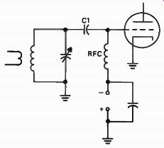
Figure 12(A). External bias.
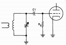
Figure 12(B). Grid-leak bias.
Grid-Leak Bias. In Fig.12(B), grid-leak bias is used. With this method of biasing, the grid current that flows during the crest of the positive half of the cycle of the incoming signal charges capacitor C1 to a high negative value. During the interval between grid current pulses, the capacitor discharges through grid-leak resistor Rg. The discharge current develops a steady negative voltage across Rg. The value of this voltage depends upon the value of Rg and on the current through it. One advantage of this circuit is that the bias adjusts itself when the driving power is changed. Increasing the driving power increases the grid current and therefore increases the voltage drop across Rg.
Thus, with grid-leak bias, changing the driving power does not appreciably change the operating angle.
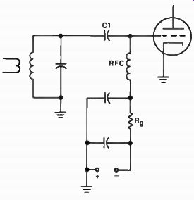
Figure 12(C). Combination external and grid-leak bias.
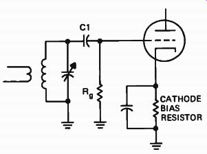
Figure 12(D). Cathode bias.
A disadvantage of using grid-leak bias alone is that if there is a failure in the preceding stage, so that no excitation is supplied to the grid of the amplifier, there will be no bias developed. Excessive plate current will then flow, and if the circuit is not suitably protected, the tube and its associated components will be damaged.
Combination External and Grid-Leak Bias. To protect the tube against loss of bias, a combination of external and grid-leak bias, shown in Fig.12(C), is often used. This circuit has the self-adjusting features of the circuit in Fig.12(B), and at the same time provides enough bias to protect the tube if there is a failure in the preceding stage.
Cathode Bias. The tube can also be protected against the loss of excitation by using the cathode bias combination, shown in Fig.12(D). The amount of protective bias, in either Fig.12(C) or Fig.12(D), is chosen so that the plate current through the tube multiplied by the plate voltage is equal to or less than the maximum safe plate dissipation of the tube. The disadvantage of cathode bias is that part of the power supplied to the plate circuit of the tube is wasted in the cathode resistor. In large high-power stages this might be a substantial amount.
Variations. The circuits in Fig.12(A) through 12(D) show the basic class C bias methods. There are also some minor variations of these circuits.
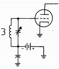
Figure 12(E). Variation of circuit shown in Fig.12(A).
For example, the circuit shown in Fig.1 2(A) may be rearranged as in Fig.12(E), eliminating the rf choke and coupling capacitor. The circuit in Fig.12(C) may be rearranged as in Fig.12(F). Perhaps we should remind you that you will find minor variations in many circuits.
Do not conclude that a circuit is necessarily different from the basic circuit you have studied just because it has been changed slightly. Study the circuit carefully and you will probably find that the method of operation is basically the same.
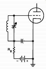
Figure 12(F). Variation of circuit shown in Fig.12(C).
AMPLIFIER STABILITY
Class C amplifiers using triode tubes will go into self-oscillation easily because of feedback between the input and output circuits. As you will learn in a later lesson, a tuned-grid, tuned-plate oscillator is simply an unstable class C amplifier.
The feedback path in a triode is through the grid-to-plate capacity. Since this capacity is quite large in a triode tube, enough energy from the plate circuit can be fed back to the grid to overcome the grid-circuit losses and cause the stage to oscillate at a frequency near the resonant frequency of the tuned circuits.
Oscillation will not take place if the plate tank circuit is tuned precisely to resonance; the tank circuit must be slightly detuned to sustain oscillation. Precise adjustment, however, is very difficult.
Even if you were able to make such an adjustment, the amplifier would be unstable. Slight changes in supply voltages and load would cause it to go into oscillation.
The feedback signal in a triode amplifier must be neutralized to prevent oscillation. The stage is neutralized by feeding a second signal back into the grid circuit. This second signal must be of opposite polarity and of the same amplitude as the signal fed into the grid circuit through the grid plate capacity of the tube in order to cancel the feedback.
The most basic method of neutralization is shown in Fig.13. In this circuit, a coil is inserted between the grid and the plate. In series with the coil is a blocking capacitor, which keeps the dc plate voltage off the grid of the tube. It has no other effect on the neutralizing circuit. The value of the coil is chosen to resonate with the grid-to plate capacity at the frequency to which the amplifier is tuned.
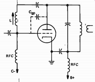
Figure 13. Neutralization for a triode tube stage.
The current through the coil lags the voltage 900; the current through the capacity leads the voltage 90°. Therefore, the currents through the coil and the capacity are 180° out of phase and cancel each other. The disadvantage of this simple and basic method of neutralization is that it must be retuned when the operating frequency is changed. Let's look at other methods of neutralization.
Plate Neutralization. Figure 14 shows plate or "Hazeltine" neutralization. In this circuit arrangement, the coil used in the plate tank circuit is tapped, and the tap on the coil is operated at rf ground potential by grounding it through the capacitor C.
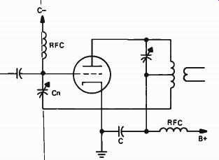
Figure 14. Plate or "Hazeltine" neutralization.
A signal voltage is developed between ground and the bottom end of the coil that is out of phase with the voltage at the plate end of the coil. By connecting the bottom of the tank circuit to the grid of the amplifier through the capacitor Cn, which is called the neutralizing capacitor, we can get a signal at the grid that will cancel the feedback from plate to grid through the tube capacity.
Capacitor Cn is adjustable so that we can apply the exact amount of signal needed to cancel out the signal fed back through the tube.
The plate neutralization system can be considered as a balanced bridge circuit. A bridge circuit is shown in Fig.15(A). The input voltage is applied between terminals A and B and the output voltage is taken off between C and D. If the ratio of impedance Z1 to impedance Z2 is equal to the ratio of Z3 to Z4, the voltage between terminals C and D will be zero, and we say the bridge is balanced.
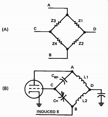
Figure 15. Equivalent bridge arrangement of plate neutralization circuit.
The plate neutralization system in Fig.14 can be redrawn as a bridge circuit as shown in Fig.15(B). The voltage is applied to terminal A from the plate of the tube. The voltage applied to terminal B is the voltage induced in the lower half of the coil in the plate circuit of the tube. We have labeled this half of the coil L2, and the upper half L1. Terminal C of the bridge is connected to the grid of the tube and terminal D is grounded. L1 is made equal to L2 by center-tapping the coil. When Cn is adjusted to equal Cgp, the ratio of LI to L2 will be equal to the ratio of Cgp to Cn. Then the bridge will be balanced, so there will be no voltage fed back to the grid circuit from the output circuit.
With this type of circuit, once the stage is neutralized it will remain neutralized over a reason ably wide frequency range, if the coil is exactly center-tapped, so that L1 is exactly equal to L2. If L1 is not exactly equal to L2, the stage can still be neutralized simply be making the ratio of the impedance of Cgp to the impedance of Cn equal to the ratio of the impedance of L1 to the impedance of L2. If there is an appreciable difference between the values of L1 and L2, the frequency range over which the stage will remain neutralized becomes limited.
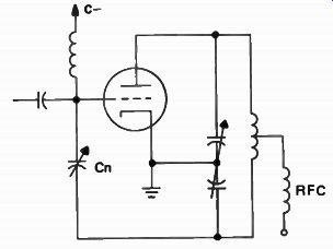
Figure 16. Another plate neutralization circuit.
Another circuit for plate neutralization is shown in Fig.16. In this circuit the center tap on the coil is not operated at rf ground potential; it is connected to B+ through an rf choke. The ground point is taken at the rotors of a split-stator tuning capacitor. A split-stator capacitor is a variable capacitor with one set of rotor plates and two sets of stator plates that are insulated from each other.
The voltages at the two ends of the coil are equal and of opposite phase. The circuit in Fig.16 can be shown as a balanced bridge by substituting the sections of the split-stator tuning capacitor for coils L 1 and L2 in Fig.15(B). The rf ground in both circuits is made through a capacitor (marked Cm Fig.16).
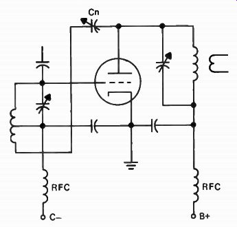
Figure 17. Grid or "Rice" neutralization.
Grid Neutralization. The tapped-grid circuit arrangement shown in Fig.17 can also be used for neutralization. This is referred to as grid neutralization or Rice neutralization. The neutralizing signal is taken from the plate and applied to one end of a tapped coil in the grid-tuned circuit. The rf ground connection is made to the center tap on the grid coil. The polarity of the feedback signal, introduced through the neutralizing capacitor Cn to one end of the grid coil, is in phase with the signal that is fed directly to the other end of the grid coil -- through the plate-grid capacity.
By properly adjusting the neutralizing capacitor Cn, voltage fed through it can be made equal to the voltage fed through the tube capacity. These two voltages will cause equal currents to flow through the grid coil in opposite directions. These currents will induce new voltages in the grid coil which will tend to cancel the voltage fed through Cn and Cg p . A split-stator version of grid neutralization is shown in Fig.18. Its operation is essentially the same as that of Fig.16.
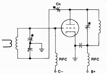
Figure 18. Split-stator grid neutralization.
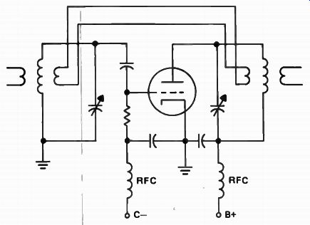
Figure 19. Inductive neutralization.
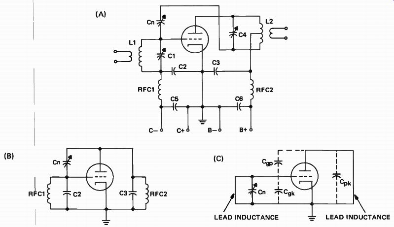
Figure 20. A typical class C stage is shown at (A); the effective circuit
that produces low-frequency parasitics is shown at (B); the effective circuit
that produces high-frequency parasitics is shown at (C).
Inductive Neutralization. Still another method of neutralization is shown in Fig.19. This is referred to as inductive neutralization, because the neutralizing signal is obtained by inductive coup ling between the plate and grid-tuned circuits. The signal induced in the grid circuit by the inductive link is opposite in polarity to the feedback signal, and gives feedback cancellation.
Parasitics. Neutralization of an amplifier is used to prevent oscillation at the frequency to which the grid and plate circuits are tuned, in other words, at the signal frequency. Some amplifiers go into oscillation at frequencies far removed from the desired signal frequency. Oscillations of this type are called "parasitic oscillations" or "parasitics."
The neutralization circuits we have just studied can do nothing to prevent this type of oscillation.
Long leads, tube interelectrode capacities, rf chokes, and bypass capacitors are the major inductive and capacitive elements that cause parasitic oscillations.
Parasitics may exist at low or high frequencies, or at both low and high frequencies at once. They cause low operating efficiency and instability in the stage, erratic meter readings, radiation of improper carriers and sidebands, distortion, over heating of the amplifier tube, and premature breakdowns in the circuit parts. If grid-leak bias is used in the stage, parasitics will also cause changes in the grid bias.
Figure 20(A) shows a typical class C amplifier stage. At the operating frequency, the grid and plate circuits are tuned by the coil and capacitor combinations L1 –C1 and L2-C4. The stage is prevented from oscillating at the operating frequency by the signal fed back through neutralizing capacitor Cn.
Figure 20(B) shows what the effective circuit would be if this stage were producing low-frequency parasitic oscillations. The grid circuit is now tuned by the parallel combination of the grid choke, RFC1, and the grid bypass capacitor, C2.
Since these oscillations usually take place at frequencies below 200 kHz, coil LI has very little reactance and serves merely as a connecting lead from the grid to the junction of C2 and RFC1.
This places the rf choke and grid bypass capacitor in parallel between grid and ground.
The tuned circuit in the plate at the low frequencies is the plate bypass C3 and the plate rf choke. Here, too, the regular tank coil L2 has practically no reactance at the oscillation frequency, and serves simply as a connecting lead.
The neutralizing capacitor Cn is now effectively in parallel with the tube grid-plate capacity and increases rather than reduces feedback. Coils L1 and L2 do have a slight reactance at the parasitic frequency, so tuning capacitors C1 and C4 can make slight changes in the parasitic oscillation frequency.
The effective circuit for the stage, if it were producing high-frequency parasitic oscillations, is shown in Fig.20(C). In this case, the grid and plate circuits are tuned by the inductance of the leads between the tube elements and the tank circuits and the grid-to-cathode capacities. At the high frequencies, the capacities of C1 and C4 are so high that they act only as connecting leads in the inductive circuit. Capacitors C2 and C3, which are even larger in size, have practically no reactance at this frequency. The neutralizing capacitor Cn now appears between grid and ground and is effective in determining the frequency of the grid circuit.
Feedback is through the capacity between grid and plate.
Preventing Parasitics. In the effective circuit of either Fig.20(B) or 20(C), parasitic oscillation can be prevented by making the resonant frequency of the grid circuit higher than that of the plate circuit.
This may be done in Fig.20(B) by making capacitor C2 smaller than C3 or by making RFC1 smaller than RFC2.
The most satisfactory method for suppressing very high-frequency parasitic oscillations in a class C amplifier stage is by using parasitic suppressors.
The purpose of these parasitic suppressors is to increase the circuit losses at the parasitic frequency. Examples of these suppressors are shown in Fig.21.
The suppressors are low resistances, usually around 100 ohms, in parallel with small rf chokes.
At the normal operating frequency, these small coils, L1 and L2, have very low inductive reactances, and the signal frequency can pass through them with no loss. At the frequency of the parasitic oscillation, however, these coils have very high reactance and force the parasitic signal to flow through resistors R1 and R2. The loss of parasitic signal in the two resistors is great enough to prevent the tube from going into oscillation at these high frequencies.
Although a commercially manufactured transmitter should be free of parasitic oscillations, occasionally a new transmitter being tuned up for the first time will have them. Parasitics can also occur if parts are replaced by those of a different make. Whenever modifications are made in an amplifier stage, that stage should be checked for both high- and low-frequency parasitics. Low-frequency parasitics will sometimes be evident as sidebands of the carrier frequency. The most common indication of high-frequency parasitics is an unusually high plate current and low output.
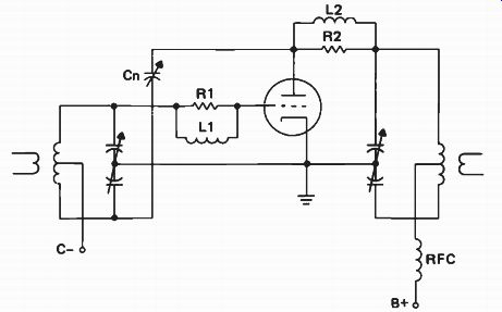
Figure 21. Parasitic suppression methods.
MULTIELEMENT TUBE STAGES
In a previous lesson you learned about the characteristics of screen-grid, pentode, and beam power tubes. Let us review briefly their characteristics with respect to their use as class C amplifiers.
If a tetrode or pentode tube is used in the stage, the screen grid of the tube acts as an electrostatic shield between the grid and plate, which reduces the grid-to-plate capacity. There fore, tetrode and pentode tubes are less susceptible to feedback and self-oscillation, and usually do not require neutralizing.
Multi-element tubes have a higher power gain than triodes. In other words, for the same amount of grid driving power, you can get a higher power output from a stage using a multigrid tube than from one using a triode. This means that fewer stages are needed to get the desired power output.
It also means that better shielding must be used between input and output circuits to prevent external feedback. Even a very small amount of feedback from the output of a stage back to the input can cause oscillation. Also, because of the higher power gain, parasitic oscillations are more common in tetrode and pentode stages than in triode stages.
In screen-grid (tetrode) class C amplifiers, the minimum plate voltage must not be allowed to swing lower than the screen voltage because the screen then offers a greater attraction to the electrons than the plate. The secondary emission effect, due to electrons bouncing off the plate and being pulled to the screen instead of falling back onto the plate, determines the minimum to which the plate voltage can swing. The grid excitation is adjusted so that the grid swings far enough positive so that the tube draws maximum permissible peak plate current without exceeding the dissipation rating of the plate and grid electrodes.
A pentode tube permits a greater plate voltage swing and, therefore, an even higher power gain. It does so by using a suppressor grid at cathode potential between the plate and screen grid to prevent secondary electrons from moving to the screen grid. Thus, the plate current remains independent of plate voltage to a much lower value of plate voltage. The suppressor grid forces the secondary electrons coming off the plate to return to the plate.
A beam-power tube has characteristics similar to those of a pentode. The tube elements are shaped in such a way that they control the electrons flowing between the cathode and the plate of the tube. Proper shaping of the electrodes sets up a potential barrier between screen and plate to suppress secondary emission.
You will find many multielement tubes used in transmitter equipment because of their higher power gain and simplicity of neutralization. Beam power tetrodes are the most common.
In many circuits using multielement tubes, no neutralization is used. However, the power gain of these tubes is so great that only a small amount of feedback will set up instability and oscillations.
Keeping feedback below the level that will cause instability or oscillation is a real problem. Even if a stage does not oscillate when it is first manufactured, there is no guarantee it will not be unstable when the tube in the stage is replaced. To overcome these problems, manufacturers often neutralize stages using multielement tubes.
In a class C stage using a multielement tube, the screen voltage has as much control, or more, on the plate current and power output as the actual value of the plate supply voltage. The plate supply voltage, however, must be high enough to obtain the necessary plate voltage swing across the plate tuned circuit. Because the screen grid has so much control, the power output in some transmitters is controlled by varying the screen-grid voltage.
The correct voltage must be applied to the plate of a multigrid tube at all times. If the plate voltage drops to zero or is lower than normal, the screen grid may be damaged. Under these conditions the screen current may be so high that it exceeds the safe dissipation factor.
Screen voltage and current also vary with the grid excitation, particularly if the screen voltage is obtained through a dropping resistor. An increase in grid excitation will cause the screen current to rise and the screen voltage to fall. A decrease in excitation will have the opposite effect.
When a tetrode or pentode stage is being tuned and loaded, the plate and screen voltages should be reduced. Most transmitters using tetrode or pentode power stages have provisions for reducing these voltages during tuning. A non-resonant or unloaded plate tank causes the minimum plate voltage to drop below the screen voltage. Under these conditions, the screen draws excessive cur rent. This may destroy high-power tetrodes in a matter of a few seconds. After the tuning and loading are roughly adjusted, full voltage can be applied to the tube and the adjustments carefully peaked.
MULTITUBE STAGES
To get a higher output from a class C stage, two tubes can be connected in parallel, or in push-pull. For very high power, tubes are operated in push-pull-parallel; that is, two sets of parallel connected tubes are operated in push-pull.
Parallel Operation. Figure 22 shows a stage with two tubes connected in parallel. In parallel operation, the output power is approximately twice that from a single tube, if the correct driving power is applied and the circuit components and electrode voltages have the correct values.
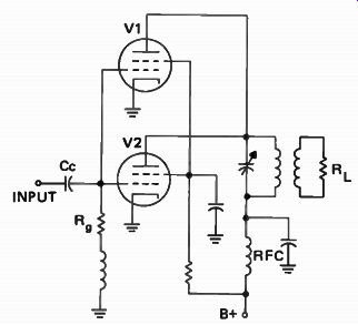
Figure 22. Class C amplifier with two tetrodes connected in parallel.
The grid current is doubled, because with two tubes the grid impedance is approximately halved.
The driving power needed for the parallel amplifier is twice that needed for a single tube.
When grid-leak bias is used with the class C stage, the value of the grid resistor must be cut in half to get the same grid bias at twice the grid current.
The internal or plate resistance is also halved because of the parallel connection and doubling of the peak plate current. Thus, the same tuned circuit voltage is developed with twice the plate current. It is the higher amplitude plate current pulses exciting the tuned circuit that develop the added power delivered to the load in parallel operation.
Push-Pull Operation. A push-pull amplifier is shown in Fig.23. The input excitation is applied with equal amplitude but opposite polarity to the grids of the push-pull stage. The ground point of the circuit is at the center of a split-stator variable capacitor.
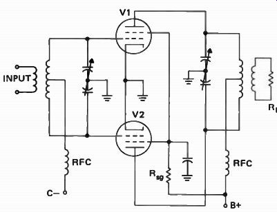
Figure 23. Push-pull class C amplifier using tetrodes.
As in the case of parallel tube operation, the grid and plate currents drawn are twice as great as those drawn by a single tube. To retain balanced operation of the push-pull stage where each tube performs an equal share of the work, the supply voltages are applied at the midpoints of the coils so as not to imbalance the stages.
Balanced operation is necessary to prevent possible overloading of one of the tubes because of any uneven dissipation of power by the grid or plate. Imbalance can be caused by tubes that are not exactly matched or by a mismatch between the grid or plate circuit components. Thus, both the circuits and the tubes must be matched and balanced to get proper operation of the stage.
FREQUENCY MULTIPLIERS
A frequency multiplier stage is a class C amplifier that is used to generate an output signal whose frequency is some multiple of the applied signal frequency. For example, the frequency of the output of a doubler stage is twice the frequency of the input. The frequency of the output of a tripler is three times the frequency of the input. A doubler with an input frequency of 10 MHz would have an output signal of 20 MHz. A tripler with an input frequency of 10 MHz would have an output signal of 30 MHz. Multipliers can be used to generate signals of even higher multiples of their input signal frequency, but the higher the multiplication the lower the output. Thus, you can expect less output from a tripler than from a doubler using the same tube type. A multiplier generating a signal four times the frequency of the input signal would have an even lower output than a tripler using the same tube.
When a tank circuit is shock-excited into oscillation by a single current pulse, the circuit will continue to oscillate for a number of cycles. The number of cycles will depend on the losses in the circuit. Each cycle will be lower in amplitude than the preceding one because of these losses. With a high Q circuit, when the losses are low, there will be many cycles before the oscillation drops to zero.
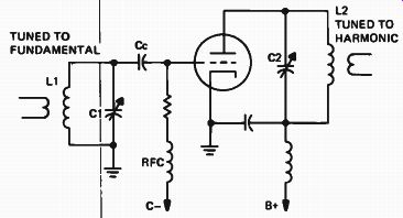
Figure 24. Basic frequency-multiplier stage.
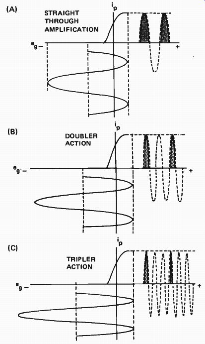
Figure 25. Waveshapes of frequency multipliers compared to- the "straight-through" amplifiers.
In a frequency multiplier we take advantage of the fact that oscillation, once started, will continue for many cycles in a tank circuit. By using a tank circuit in the plate circuit of the tube that is resonant at some multiple of the input frequency, we can start the oscillation by feeding an rf signal to the grid. This will produce a plate current pulse that starts the tank circuit oscillating at its resonant frequency which may be two or three times the frequency of the input signal. This oscillation would soon die out, except on the second cycle in the case of a doubler, or the third cycle in the case of a tripler, where the grid of the tube will be driven positive again by the rf signal. This produces another plate current pulse which adds to the energy in the tank circuit and supplies the power needed to make up the circuit losses, so the oscillation in the plate circuit continues. Now let's look at some typical frequency multiplier circuits.
Single-Tube Multipliers. The circuit of a frequency multiplier is very simple; one is shown in Fig.24. It is even simpler than a regular class C amplifier. No neutralization is needed, even when the tube used is a triode, because self-oscillation occurs only if the input and output circuits are tuned close to the same frequency. In a doubler the output tank circuit is tuned to twice the frequency of the input circuit, in a tripler it is tuned to three times the frequency, etc.
The current waveforms in the tank circuit of a class C amplifier are compared with those in a frequency multiplier in Fig.25. Figure 25(A) shows the waveforms for a fundamental class C amplifier.
The plate current pulse flows during part of each cycle of the incoming signal. The flywheel action of the tank circuit develops the fundamental sine wave output, shown by the dashed curve.
Figure 25(B) shows the waveforms for a single-tube doubler circuit. The tube is operated with a higher bias, so the plate current pulse flows during a smaller part of each cycle of the incoming signal, and the flywheel action of the resonant circuit carries through that cycle and another cycle before the next plate current pulse arrives. Since the plate current flows only on alternate cycles of the output, the power output and efficiency of the stage are lower than for fundamental operation.
The efficiency is usually less than 50%. The higher the harmonic signal to which the tank circuit is tuned, the lower the obtainable power output and efficiency of the class C stage.
Figure 25(C) shows the waveforms for a tripler.
The tube is biased so that the plate current flows for a still smaller part of the cycle of the incoming signal, and the resonant circuit carries through three cycles before the next pulse arrives. Losses in the circuit cause the amplitude of each succeeding cycle to decrease. The efficiency of a tripler stage is even less than that of a doubler. The efficiency of a multiplier is kept as high as possible by using the proper values of L and C in the tank circuit and correctly shaping the plate current pulse.
The best pulse shape is a square top pulse like the ones shown in Fig.26. This pulse shape can be obtained by operating the stage with a high bias and then driving the stage to plate-current saturation. For best doubler operation, the angle of current flow, indicated by the Greek letter O (theta), should be somewhere between 90 and 120 degrees. With this angle of flow, the plate current pulse has a suitable and effective second harmonic content. For tripler operation, the angle of current flow is reduced to less than 90 degrees, and the third harmonic component is emphasized.
The plate tank circuit of frequency multipliers can usually be tuned over a wide enough range to resonate at more than one harmonic of the signal at the grid. Therefore it is important that you check the output frequency to be sure you have the correct harmonic. You can do this with an absorption wavemeter. You'll learn more about this instrument later in the lesson.
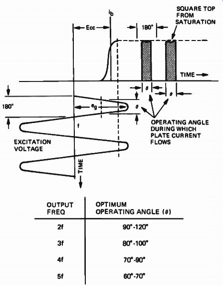
Figure 26. Multiplier operating characteristics.
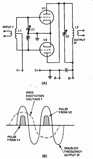
Figure 27. Push-push doubler for even harmonics.
Two-Tube Multipliers. A special higher powered and somewhat more efficient doubler can be obtained by using the push-push arrangement shown in Fig.27(A). In this circuit, the grids are supplied with signals in push-pull and the plates are connected in parallel.
The tubes are connected so that one will conduct on the positive alternation of the incoming signal, shown in dashed lines in Fig.27(B), and the other tube will conduct on the negative alternation. Thus, plate current pulses are fed to the output circuit once during each alternation of the doubled frequency. The efficiency and power output are higher than for a single-tube doubler.
The push-push frequency multiplier stage in Fig.27(A) operates well on even harmonics, but not on the fundamental or odd harmonic frequencies. Frequency doublers are used more often in transmitters, especially low-frequency transmitters, than the higher harmonic generators because of the higher output and efficiency. The grids are connected in push-pull, so they must be fed with balanced signals to get the proper output signal.
Since the doubler is the most frequently used type of frequency multiplier stage, let us list some of its characteristics:
1. The plate tank circuit is tuned to twice the grid circuit frequency.
2. It does not have to be neutralized.
3. The operating angle of the plate current pulse is approximately 90°.
4. The dc bias is about 10 times the plate current cutoff value.
5. The plate current pulse has a greater harmonic content.
6. It requires a very large grid-driving signal.
7. It has a low plate efficiency compared to a fundamental class C amplifier.
As you can see, some of these characteristics vary widely from those of a class C amplifier operating as a fundamental frequency amplifier.
SELF-TEST QUESTIONS
12 What is the disadvantage of using only grid leak bias in a class C amplifier?
13 What is the feedback path for oscillations near the operating frequency in a triode class C amplifier?
14 What is the main advantage of plate neutralization over the method of connecting a coil and blocking capacitor from plate to grid?
15 In Fig.16, what is the phase relationship between the signal fed through Cn and the signal fed back through grid-plate capacitance?
16 What inductive components in the grid circuit form part of the low-frequency parasitic resonant circuit?
17 What might be the cause of unusually high plate current and low if output from a transmitter?
18 What two characteristics of tetrodes make them more useful as class C amplifiers than triodes?
19 What characteristic of tetrodes makes them more susceptible to parasitic oscillation than triodes?
20 How would the values of L and C in a tank used in a parallel-connected stage compare with those used in a similar single tube circuit operating at the same frequency?
21 How is balanced operation obtained in a push-pull stage?
22 In general, which multiplier would have a higher output, a doubler or a tripler?
23 Why are neutralization circuits unnecessary in a triode operated as a frequency multiplier?
---------------
Transistor Power Amplifiers
In their present state of development, transistors cannot amplify high-frequency signals to high power levels as well as vacuum tubes. However, power outputs greater than 100 watts or frequencies much above 900 MHz are seldom required in many communications applications. Chief among these is commercial mobile radio. In this application, the transistor's small size, low operating voltage, extreme ruggedness, and high overall efficiency make it ideally suited for use in mobile radio equipment.
The common emitter circuit is almost universally used for transistor rf power amplifiers because of its greater stability at radio frequencies. This circuit arrangement is often compared with the grounded cathode triode. As you might expect, it has much in common with the triode circuits you previously studied. With transistor amplifiers we are concerned with the biasing, efficiency, and stability, just as we were with the triode. In this section, we'll look at some typical circuits which illustrate the important features of transistor rf power amplifiers.
BIASING METHODS
You have learned that class C operation of a power amplifier results in the highest percentage of input power being converted to useful rf energy at the output. In the case of a transistor, where high-frequency power handling is a limitation, we are especially interested in getting the highest efficiency obtainable from the stage. It is not surprising then that most transistor rf amplifiers are operated class C. Two practical methods of obtaining bias for class C operation are shown in Fig.28. The 'circuits illustrated employ npn transistors; pnp devices could just as well have been used (with all polarities reversed, of course).
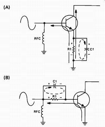
Figure 28. Methods of obtaining emitter-base reverse bias.
In Fig.28(A), reverse bias across the emitter base junction is developed by the R1-C1 network in the emitter circuit. When the input signal to the stage goes sufficiently positive, base and collector currents flow over the paths indicated by the solid lines. Both these currents flow through the emitter resistor, dropping a voltage of the polarity indicated. Capacitor C1 charges to the peak value of this voltage drop. During the time between positive going portions of the input signal, C1 slowly discharges through R1 as indicated by the dashed line. The values of R1 and C1 are such that C1 does not discharge appreciably before the input signal again swings positive, thereby recharging C1.
The emitter is thus maintained slightly positive with respect to the base by the charge across C1.
Collector current does not flow until the input signal drives the base more positive than the emitter.
Reverse bias for the circuit of Fig.28(B) is developed in the base circuit, again by a parallel combination of R1 and C1. The base current drawn during the positive-going portion of the input signal (indicated by the solid line) drops a voltage across R1 as shown. C1 charges to the peak value of this voltage drop and essentially maintains its full charge during the time between positive going portions of the input signal. This is possible because the discharge path for C1 (shown by the dashed line) is through R1, the value of which is chosen to permit only a very small discharge current to flow. Notice that the polarity of the charge on C1 is such that it subtracts from the positive-going portion of the input signal. This means that the input signal voltage must exceed the voltage across C1 before the emitter-base junction becomes forward-biased, allowing collector current to flow.
The two circuits shown in Fig.28 depend on the presence of an input signal to develop bias.
With no input signal present, zero bias is develop ed. Unlike vacuum tubes, however, transistors do not conduct under zero bias conditions and are therefore self-protecting.
Not only are transistors nonconducting under zero bias conditions, but also a small forward biasing voltage must exist across the emitter-base junction before collector current begins to flow.
Figure 29 shows collector current plotted against emitter-to-base voltage for a typical rf power transistor.
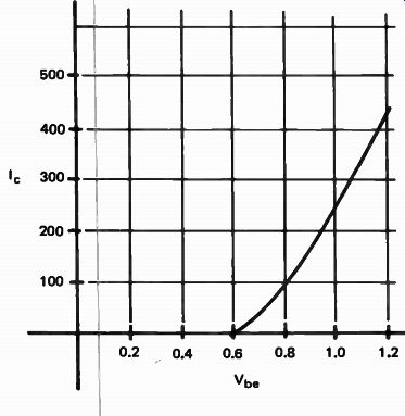
Figure 29. Collector current plotted against emitter-to-base voltage of
a typical rf power transistor.
As you can see from the graph, collector current does not begin to flow until the emitter base voltage reaches approximately 0.6 volt. When we operate a power transistor with zero bias, then, we are actually biased about 0.6 volt below collector current cutoff.
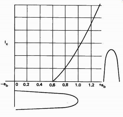
Figure 30. Curve of Fig.29 with signal applied showing collector current
pulse.
Figure 30 shows the graph of Fig.29 with an input signal of 1 volt peak amplitude applied.
Collector current flows only during the time the input signal is above 0.6 volt. The conduction angle here would be about 120° of the input cycle, well within the class C operating range. Input signal levels of such low amplitude are not unusual in power transistors because of the transistor's low input impedance. Input impedances actually range from several ohms to less than 1 ohm. With such a low input impedance, a relatively large input current is permitted to flow when the base-emitter junction of the transistor is driven positive.
Recalling that P = EI, you can readily see that the driving power to the stage is accounted for primarily by the high current flow which develops only a small voltage across the low input impedance. It follows, then, that a reverse-biased emitter-base junction is not always necessary for class C operation.
MULTI-TRANSISTOR AMPLIFIERS
As mentioned earlier, the power obtainable from a transistor used as an rf amplifier is rather limited as compared to vacuum tubes used in similar circuits. When more power is required than can be obtained from a single transistor, several transistors can be arranged in push-pull or parallel.
In a push-pull arrangement, an input transformer is required to feed out-of-phase signals to the transistors. This transformer is also required to match the relatively high output impedance of the driver to the very low input impedance of the push-pull stage. Such a transformer capable of operation at high frequencies is very expensive to build. For this reason, multiple transistor stages are nearly always parallel-connected.
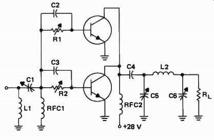
Figure 31. Two-transistor parallel-connected rf amplifier.
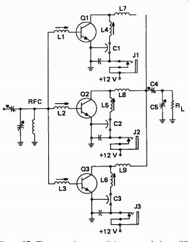
Figure 32. Three-transistor parallel-connected rf amplifier.
Figure 31 shows a two-transistor parallel connected rf amplifier stage. C1 and L 1 form an L network which provides the proper impedance match between the source and the input to the stage. The input signal is developed across RFC1, amplified by the transistors, and applied to the load through the output coupling network. Notice that we can vary the operating bias of the two transistors by adjusting R1 and R2. These adjustments are necessary so that the two transistors will share the load equally. In practice we would insert a milliammeter in the collector or emitter circuit of each transistor and adjust R1 and R2 for equal currents. With the current balanced, each transistor will be handling half of the power delivered to the output coupling network. C4 is a coupling capacitor and may be considered a short circuit at the operating frequency. The output coupling circuit is a pi network consisting of C5, L2, and C6. C5 and C6 are adjusted to provide the proper collector load and circuit Q for the transistors.
Another circuit employing transistors in parallel is shown in Fig.32. Besides containing three transistors instead of two, this circuit differs from the one in Fig.31 in two other important respects.
First of all, load balancing is obtained by adjusting L1, L2, and L3 in the base circuits. These adjustments vary the rf drive to the transistors and equalize the load currents as previously discussed.
Secondly, each of the three transistors in Fig.32 has a separate output tank circuit connected to a common load as in Fig.31.
The tank circuit for Q1 is made up of L4, L7, and stray capacity. L5 and L8 are the tank inductances for Q2; L6 and L9 are the tank inductances for Q3. .These tank circuits are also tuned by stray capacity. The right-hand ends of L7, L8, and L9 connect to C4 which, along with C5, varies the coupling from the three tank circuits to the load RL. There are two reasons why separate tank circuits are used for the three transistors. First, each transistor is series-fed, thus eliminating the losses and other problems of an rf choke. Second, the dc collector currents are entirely separate so each transistor can operate essentially independent of the other transistors. Thus, if some trouble developed in Q!, this stage could be disconnected and the amplifier could continue to operate at a lower power level. Directly paralleled stages would have to be completely retuned if one stage were to be removed.
Many rf power transistors have their emitters internally connected to the transistor case. This is done to eliminate the stray inductance of the emitter lead. When the case is connected to ground, as it would be in a circuit such as that shown in Fig.32, current could not be conveniently measured in the emitter circuit. The use of separate collector loads, however, enables convenient monitoring of collector current. In Fig.32, the jacks labeled J1 through J3 are provided for this purpose.
The symbol used to represent C1 through C3 may be unfamiliar to you. This is a special type of capacitor called a feedthrough and is often used for bypassing in high-frequency circuits. As the symbol suggests, one plate of the capacitor completes a dc path in the circuit; the other plate, usually connected to ground, surrounds the first much like the braided shield in a piece of coaxial cable.
FREQUENCY MULTIPLIERS
Figure 33 shows two transistor frequency multiplier stages coupled together. The output of the tripler, Q 1 , feeds a doubler, Q2, to give a total frequency multiplication of six. The input signal, which we've designated as Fo, is applied to the base of Q1 . With the drive signal present, R1 and C1 develop a relatively high reverse bias across the emitter-base junction. The high reverse bias results in a narrow conduction angle and collector current pulses with a high harmonic content. The collector tank is tuned to the third harmonic, 3Fo, and offers a high impedance only at this frequency.
Signals at the fundamental, as well as those at other harmonics, are bypassed to ground by C2 and C3. The signal at the frequency 3Fo is inductively coupled into the base circuit of Q2.
Reverse bias for Q2 is developed by the driving signal in a manner similar to that described for Q1.
The collector tank for Q2 is tuned to 6Fo and inductively couples the signal at this frequency into the load. Undesired signals are again bypassed to ground, in this stage by C5 and C6.
While individual stages are seldom designed for frequency multiplications greater than three, any desired total multiplication may be obtained by connecting multipliers together. The usual arrangement in a transmitter is a straight-through class C amplifier following each one or two multiplier stages. In this manner, the relatively low output from the multiplier is built up before being applied to the next multiplier. The straight-through amplifier also offers additional suppression to the undesired harmonics generated in the multiplier stage.
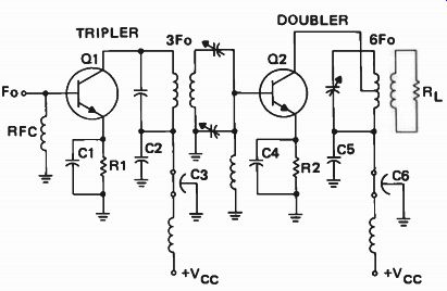
Figure 33. Two frequency multiplier stages coupled together.
AMPLIFIER STABILITY
You learned that, in the triode power amplifier, in-phase feedback through plate-to-grid inter electrode capacitance could cause the amplifier to oscillate. To prevent these oscillations from occur ring, components were added to feed back an out of-phase voltage of equal amplitude and thus "neutralize" the interelectrode capacitance of the tube.
A similar capacitance exists between the collector and base of a transistor. However, the value of this collector-to-base capacitance in power transistors is voltage-dependent. That is, as the reverse bias across the collector-base junction varies (which it normally does over the period of an operating cycle) the collector-to-base capacitance also varies.
To be effective, a neutralizing circuit for a power transistor would have to continuously adjust itself to this variation. Because of this requirement, neutralization of a transistor rf amplifier is normally not practical. Instead, the need for neutralization is usually eliminated by careful circuit design using transistors with low values of inter-element capacitance.
Parasitics. In the radio frequency range, the power gain of a transistor falls off rapidly as frequency increases. This characteristic of transistors works to advantage in preventing parasitic oscillations above the operating frequency. At these higher frequencies, the transistor has insufficient gain to overcome the circuit losses and sustain oscillations.
On the other hand, the power gain of a transistor is higher at the lower frequencies. To illustrate this, let's assume we have an rf power amplifier operating at 175 MHz. A typical transistor operating at this frequency might have a power gain of 5 db. This same transistor could have a gain as high as 30 db at 10 MHz. In other words, the power gain of the device is over 300 times greater at 10 MHz, the parasitic frequency, than at 175 MHz, the operating frequency. Consequently, the most common cause of instability in these power amplifiers is parasitic oscillation below the opera ting frequency.
The amplifier circuit shown in Fig.34 illustrates a number of techniques used to prevent low frequency parasitics. These are discussed in the following paragraphs.
The rfc connected between base and ground (1) will at some frequency form a parallel-resonant circuit with the emitter-base capacitance. To decrease the efficiency of this parasitic tank circuit, the rfc is designed to have a very low Q (high effective series resistance). Often this rfc is nothing more than a wire-wound resistor.
The emitter bypass capacitor (2) used is the smallest value which will provide effective bypassing at the operating frequency. At frequencies below the operating frequency, the reactance of this capacitor increases, resulting in degenerative feedback at these lower frequencies. This degeneration reduces the gain of the amplifier to low frequency parasitics.
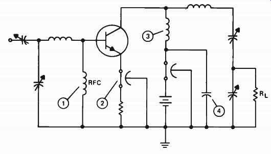
Figure 34. Transistor power amplifier showing components used to prevent
low-frequency parasitics.
The output coupling network is designed to include a portion of the network inductance in the collector dc supply line (3). With this arrangement, no rfc is required in the collector circuit. Elimination of the collector rfc is desirable because this component can form a parallel-resonant circuit with the output capacitance at some relatively low frequency, thus becoming a possible source of low-frequency parasitics.
In addition to the feedthrough capacitor designed to bypass the power supply at the operating frequency, a second capacitor of larger value (4)
provides a short circuit to ground at lower frequencies where parasitics usually occur. You might wonder why a larger capacitor, since it bypasses well at lower frequencies, wouldn't provide an even better bypass at the operating frequency where its Xc would be even less. The reason is that at higher radio frequencies the inductive reactance of the capacitor's leads becomes significantly large. The capacitor, instead of being a short circuit to ground, becomes an impedance to ground at these higher frequencies. The feedthrough capacitor, be cause of its physical construction, has very low lead inductance, and therefore provides an effective short circuit to ground at the high operating frequency. Feedthrough capacitors can only be manufactured with comparatively small values of capacitance, hence the need for the more conventional larger capacitor for the low-frequency bypass.
HIGH-FREQUENCY LOW-FREQUENCY EQUIVALENT
EQUIVALENT
Figure 35. Equivalent circuits for the power supply by passing arrangement shown in Fig.33.
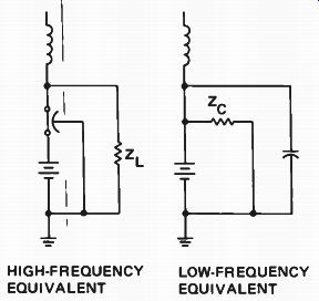
Figure 35 summarizes what we have said about power supply bypassing. Shown
in the figure are the equivalent bypass circuits for both the high operating
frequency and the low parasitic frequency. At the operating frequency, the
larger capacitor appears as an inductive reactance, ZL, and the feedthrough
as an ac short circuit to ground. At a low parasitic frequency, the feed
through appears as a high capacitive reactance, Zc , and the larger capacitor
provides the ac short to ground.
SELF- TEST QUESTIONS
24 Which transistor circuit configuration has the greatest stability at radio frequencies?
25 What happens when loss of drive causes the bias on a transistor rf amplifier to drop to zero?
26 Is reverse bias on the emitter base junction necessary for class C operation in a transistor rf amplifier?
27 What characteristic of transistor rf power amplifiers accounts for the low signal voltage developed in the input circuit?
28 Why is a parallel connection of transistors favored over a push-pull connection?
29 What are two advantages of having separate collector tank circuits for a parallel-connected transistor rf amplifier?
30 Why are feedthrough capacitors used for bypassing in high-frequency circuits?
31 What characteristic of power transistors makes neutralization impractical? 32 What is the most common form of transistor rf amplifier instability?
33 Why is an additional capacitor placed in parallel with the feedthrough capacitor by passing the power supply in Fig.32?
----------------------
Adjusting Class C Amplifiers
Adjustments to class C amplifiers in transmitter stages are performed following repairs or routinely to compensate for normal circuit aging. The adjustment procedures for all class C stages, either frequency multipliers, intermediate amplifiers, or power output stages, are basically the same. There are variations, of course; when you tune a frequency multiplier, for example, you must make certain that the plate circuit is tuned to the desired harmonic frequency.
In this section, we will go through the complete adjustment procedure for both a vacuum tube and a transistor class C amplifier stage. You should realize that adjustments such as those described in this section may be performed only by a person having the necessary authority. To obtain this authority, he must hold the proper class of FCC License or be under the direct supervision of another person who does.
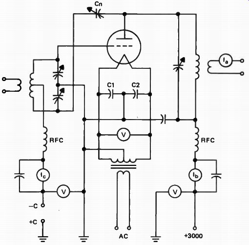
Figure 36. Typical class C amplifier.
THE VACUUM TUBE STAGE
Figure 36 shows a typical class C amplifier circuit. Notice that there are current meters in the grid and plate circuits and that voltmeters are used to measure the bias, filament, and plate supply voltages. A power output stage using a screen-grid tube often has a current meter and voltmeter in the screen circuit. In some rf output stages, particularly in the low power exciter stages, only one voltmeter and one or perhaps two current meters are used. These meters are switched into the various stages to check the performance of the stage during operation or during the adjustment procedure.
Neutralization. The first step in the adjustment procedure is to check that the amplifier is properly neutralized. Always check for neutralization with all interstage shields in place. If the amplifier is enclosed in a separate shield box within the transmitter cabinet, check it with the shield box closed. There will probably be stray magnetic or electrostatic coupling between output and input circuits unless all shields are in place and closed.
Neutralization can correct only for capacitive coupling directly from the grid to the plate of the tube. The simplest indication which can be used to determine correct neutralization is the grid current meter. With B+ removed from the stage, the need for neutralization will be indicated by a dip in the grid current when the plate tank is tuned through resonance. The grid current dips because the power loss in the resistance of the plate tank is greatest at resonance. Since this power is fed into the plate tank through the grid-plate capacitance, it sub tracts from the grid current and causes a dip.
A second, more sensitive method of checking for correct neutralization is by use of a wavemeter.
As shown in Fig.37, this simple device consists of a parallel LC circuit connected to a diode and dc milliammeter. The variable capacitor, which is calibrated in units of frequency, may be adjusted to make the circuit resonant over a wide range of frequencies. Any energy coupled into the tank circuit is rectified by the diode and causes the meter to deflect. In use, the wavemeter is inductively coupled to the plate tank circuit of the stage to be checked.
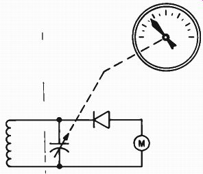
Figure 37. Simplified schematic diagram of a wavemeter.
With plate voltage removed and grid drive applied to the stage, there should be no indication on the meter as the tuning knob is adjusted near the operating frequency. An indication on the meter indicates the presence of rf in the plate tank.
This rf could only have come from the grid circuit, coupled through inter-element capacitance to the plate tank. Hence, the stage must be neutralized.
The procedure to be used in neutralizing an amplifier is as follows:
1. Remove the B+ from the stage. Never attempt to neutralize an amplifier with the plate voltage connected
2. Set the neutralizing capacitor for minimum capacity.
3. Apply filament power and bias to the stage, and apply filament power, bias, and B+ to all stages ahead of the stage being neutralized.
4. Tune the grid circuit to resonance as indicated by maximum grid current.
5. Tune the plate tank circuit to resonance while watching the neutralization indicator. If it is a grid meter, it will dip; if you are using a wavemeter, it will peak.
6. Increase the capacity of the neutralizing capacitor slightly. Check grid and plate resonance; changing the neutralizing capacitor will sometimes detune both grid and plate circuits.
7. Continue to increase the neutralizing capacitance in small steps until there is no dip in the grid meter or no indication of power in the plate tank.
The transmitter is then correctly neutralized.
As you come closer and closer to neutralization, make smaller and smaller changes in the neutralizing capacitor. There is only one correct setting; too much or too little capacitance are equally bad. Remember to retune both grid and plate each time you change the neutralizing capacitor. If the transmitter uses inductive link neutralization, start with maximum coupling to this link.
Then reduce the coupling in small steps until you find the correct coupling.
Neutralization must be made as accurately as possible. Although steady oscillation will take place only when enough power is fed back from the output to overcome the input circuit losses, smaller amounts of feedback, which are not enough to cause steady oscillation, can still affect the operation of the stage. An amplifier operating like this is said to be "regenerative." Several characteristics of an amplifier change when it is regenerative. One of the most pronounced is an increase in input impedance. This increase in impedance causes the Q of the grid and plate tuned circuits to increase also. The increase in Q makes the circuits selective and hard to tune. To make matters worse, changes in the plate tuning change the amount of feedback and, therefore, affect the grid tuning.
A regenerative amplifier is an unstable amplifier. A slight increase in filament current or plate voltage may cause it to go into steady oscillation.
Reducing the load at the output will also cause oscillation.
In a keyed transmitter, a regenerative amplifier will cause damped oscillations every time the key is closed. As a result, undesirable signals are genera ted. In a phone transmitter, an unstable amplifier causes still other effects.
Perfect neutralization of an amplifier is absolutely necessary. It takes time to do it right, but it does not have to be done often.
After you have completed the neutralizing procedure, apply a low plate voltage to the stage.
Tune the plate tank capacitor to resonance as indicated by minimum plate current readings. You will notice that the plate current will dip sharply because the output tank circuit is not delivering power to the load. This is shown by the solid curve in Fig.38.
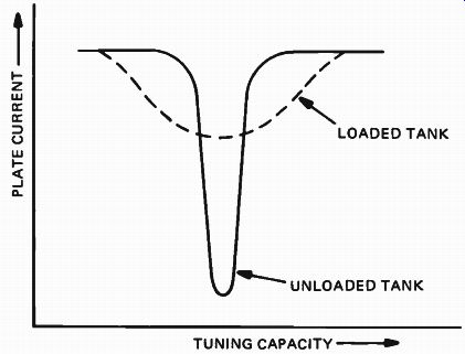
Figure 38. How plate current dips as tank capacitor is tuned through resonance;
the unbroken line shows the sharp dip that occurs if the tank is not loaded;
the dashed line shows the broad dip that occurs if the tank is loaded.
The grid current meter will indicate maximum at resonance. Retune the grid tank capacitor, and increase the excitation until the grid draws the rated current.
Increase the loading in the plate tank circuit until any increase in loading causes the current through the antenna meter to drop. Increase the loading in steps. Check the plate circuit tuning for resonance each time you increase the load. Now apply the plate voltage and adjust it to the rated value.
Retune the plate tank to resonance, and then advance the loading until the tube draws the rated plate current. The minimum plate current point will not be as sharp because the tuned circuit is now loaded and more power is being fed into the load circuit. The loaded plate current tuning curve is shown by dotted lines in Fig.38. Adjust the grid tank and excitation until the rated grid current is drawn.
Make final fine adjustments to the plate tuning and antenna loading. Be certain all meters show the recommended values for proper operation of the stage.
The output is indicated by the current readings on the rf antenna current meter. As the stage is resonated and the loading is increased, the antenna current increases, indicating power is being delivered to the antenna. The antenna meter is just as important as the plate ammeter when tuning. If the output current does not increase when the plate current increases, the plate circuit is not tuned to resonance or is overloaded. Reduce the coupling and retune the plate tank.
Parasitics. It is interesting to note that the wavemeter is also useful in detecting the presence of parasitics in the operating amplifier. As you know, these oscillations take place at a frequency far removed from the operating frequency. The most practical way to locate the oscillations is to reduce the bias of the stage so that the tube is no longer operated beyond plate-current cutoff. Then reduce the plate voltage so that the maximum plate dissipation of the tube is not exceeded. Disconnect the output and remove the drive from the stage.
These changes make the circuit most favorable for the generation of parasitic oscillations.
With the wavemeter inductively coupled to the circuit suspected of oscillating, the wavemeter tuning knob is varied over its range. A meter deflection not only indicates parasitic oscillation, but the frequency may be approximately deter mined by the position of the tuning knob. Knowing the frequency at which parasitics are occurring often provides a clue to their origin.
THE TRANSISTOR STAGE
The transistor power amplifier, although used to some extent in low-level fixed station and broadcast transmitters, finds its widest application in low-powered mobile transmitting equipment.
Since these units are operated largely by non technical people working under less than ideal conditions, the emphasis in their design is on simplicity and reliability. Because of this emphasis, adjustment procedures for transistor class C amplifiers are usually simple and straightforward. The complete transmitter alignment of many of these units consists in its entirety of peaking the indication on a power output measuring device with as few as two transmitter adjustments.
Even in the more elaborate transmitters you'll seldom find more than one meter built into the equipment. This single meter is switched into the various points in the circuit where current or voltage is to be measured. Sometimes, all the monitoring points in the circuit are connected to a multipin jack on the transmitter chassis. When transmitter adjustments are to be made, an external meter equipped with a selector switch is plugged into this jack for monitoring.
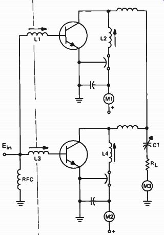
Figure 39. Parallel-connected transistor stage.
Figure 39 shows a parallel-connected output stage such as might be found in one of the higher powered transistor transmitters. We have shown separate meters at the various monitoring points for clarity. Before applying power to the amplifier, L1 and L3 should be adjusted for minimum drive to the transistors (adjusted for maximum inductance). With this accomplished, apply power and adjust the collector circuit of Q1 to resonance.
This is done by adjusting L2 for a dip on M1.
In like manner, adjust the collector circuit of Q2 to resonance using L4 and M2. Next, adjust the coupling to the load using C1 to obtain the rated load current as measured on M3. Finally, adjust the base drive to the transistors using L1 and L3 to obtain equal collector currents at the rated value.
This completes the preliminary adjustment of the stage. Since there is some interaction between the various adjustments, recheck the setting of L2, L4, and C1. At all times maintain the collector currents at or below the rated value by adjusting L1 and L3.
In conclusion, the adjustments we've discussed in this section should not be considered as a procedure to be memorized and followed in any specific case. They are presented here to illustrate the basic approach to power amplifier adjustment.
Before attempting any adjustment to a power amplifier, carefully consult and follow the manufacturer's literature. In making the adjustments, both the procedure and the sequence in which the steps are performed are of the greatest importance.
An expensive tube or transistor may be destroyed as a result of any adjustments performed without complete knowledge of the correct procedure.
SELF-TEST QUESTIONS
34 How may a vacuum tube stage be checked for proper neutralization using the grid current meter as an indicator?
35 Why must B+ first be removed from a stage before checking the plate tank for the presence of rf?
36 What are some indications of a regenerative amplifier?
37 What tuning defect is indicated if the antenna current does not increase with an increase in plate current?
38 Why is the drive to the transistor amplifier in Fig.39 adjusted for minimum before collector power is applied?
ANSWERS TO SELF-TEST QUESTIONS
1 Because output current flows in the amplifier only during the relatively brief conducting period.
2 Both the bias level and the amplitude of the driving signal affect the operating angle.
3 No. Sometimes high power gain in an amplifier, obtained with a matched load, must be sacrificed for greater power output.
4 The values of L and C would both have to be changed. L would be increased and C de creased.
5 The loaded Q would decrease. The unloaded Q would be unaffected. The efficiency of the tank would increase.
6 If the loaded Q decreases, the reflected resistance in the tank must have increased.
The increased resistance in the tank causes tank impedance to decrease.
7 By offering a high impedance only at the resonant frequency.
8 By decreasing the spacing between the coils.
9 Since the power supply, the tank, and the stage are in series, the amplifier is series-fed.
10 The output connection to the tank could be tapped down on the tank coil, as shown in Fig.9(C). This causes the internal resistance of the stage to appear to the tank as a higher value. This higher resistance seen by the tank reflects a higher resistance into the tank which increases the loaded Q.
11 An antenna usually loads a power amplifier more heavily than the input circuit to another class C amplifier.
12 If the drive to the stage is lost, no bias will be developed, allowing the tubes to conduct heavily. This heavy conduction could damage the tube.
13 Through the plate-to-grid capacitance.
14 Plate neutralization is effective over a range of frequencies, whereas the blocking capacitor and coil arrangement is effective only at one frequency.
15 180°. The signal fed back through a neutralizing circuit will always be 180° out of phase with the signal fed back through the grid to plate capacitance.
16 Radio frequency choke and bypass capacitor.
17 Parasitic oscillations in the amplifier.
18 Their higher power gain and reduced grid-to plate capacitance.
19 Their higher power gain. Even a very small amount of feedback may cause the tetrode to oscillate.
20 The value of L would be lower and the value of C higher. This would provide the lower value of tank impedance necessary for the parallel-connected tubes.
21 By connecting the supply voltages to the midpoints of the tank coils.
22 The doubler. In general, the greater the frequency multiplication in a stage, the lower the power output.
23 Since the output frequency is different from the input frequency, any signal fed back would not add to the input signal.
24 The common emitter.
25 The transistor stops conducting.
26 Not always. A zero-biased transistor is already several tenths of a volt below collector cur rent cutoff.
27 The low input impedance of the amplifier.
28 Because of the expense of the transformer required to drive a push-pull stage.
29 RF choke losses are eliminated and the transistors are electrically independent.
30 Because they have a very low lead inductance.
31 The collector-base capacitance varies over the period of an operating cycle. Thus a varying amount of signal is fed back to the input.
32 Low-frequency parasitics. The power gain of a transistor increases rapidly as frequency de creases. For this reason, a transistor amplifier is most susceptible to low-frequency parasitic oscillations.
33 Because of their physical construction, feed through capacitors cannot be manufactured with high values of capacitance. Proper bypass at low parasitic frequencies requires a large capacitance, so another type must be connected in parallel with the feedthrough.
34 With plate voltage removed, a dip in grid current when the plate tank is tuned through resonance indicates the need for neutralization.
35 With the B+ on the stage, rf in the tank circuit is a normal indication.
36 Changes in plate tuning affect grid tuning.
Also, oscillations occur with reduced loading or slight changes in operating voltages.
37 The plate tank is not tuned to resonance or is too heavily loaded.
38 To prevent possible excessive collector cur rent flow due to the low impedance offered by the detuned output circuit.
Lesson Questions
Be sure to mark your lesson card as shown to indicate Lesson CC204. Most students want to know their grades as soon as possible, so they mail their lesson card in immediately. Others, knowing they will finish another lesson within a few days, send in two cards at once. Either practice is acceptable. However, don't hold your answers too long; you may lose them. Don't hold answers to more than two sets of lessons at one time, or you will run out of lessons before new ones can reach you.
1. A buffer amplifier is needed in a transmitter to:
a. Isolate the multiplier and final.
b. Prevent parasitic oscillation.
c. Provide proper drive for the oscillator.
d. Present a light, constant load to the oscillator.
2. Which type of amplifier would most likely require neutralization?
Tetrode.
Pentode.
Beam tetrode.
Triode.
3. If a class C amplifier has a measured power output of 500 watts and operates with 2000 volts plate voltage and 330 ma plate current, how much power do the tube and plate tank circuit together dissipate?
a. 160 watts.
b. 330 watts.
c. 420 watts.
d. Not enough information to determine.
4. What is the approximate efficiency of the amplifier of Question 3?
a. 25%.
b. 50%.
c. 76%.
d. 85%.
5. If a transmitter output frequency of 26.4 MHz is obtained by using a tripler and a doubler, what is the master oscillator frequency?
2.2 MHz.
4.4 MHz.
8.8 MHz.
14.2 MHz.
6. With respect to a straight class C amplifier, the bias of a frequency multiplier is:
a. Much less.
b. Slightly less.
c. Much more.
d. Slightly more.
7. If the plate current of a class C amplifier using grid-leak bias suddenly rises and the power output drops, the probable cause is:
a. Loss of grid drive.
b. A shorted load.
c. An open load.
d. Poor power supply regulation.
8. In what frequency range would you expect to find parasitic oscillations in a transistor rf amplifier?
a. Low frequencies.
b. At the operating frequency.
c. Frequencies higher than the operating frequency.
d. Transistor amplifiers are not subject to parasitics.
9. A Faraday screen:
a. Is the third grid in a pentode.
b. Is needed only at higher frequencies.
c. Reduces transfer of harmonics.
d. Cannot be used with link coupling.
10. The method usually used to obtain higher output from transistor rf amplifiers is to use:
a. Larger transistors.
b. A push-pull connection.
c. A common base circuit.
d. Parallel-connected transistors.
Based on: NRI Schools (courses)-- A Division of The McGraw Hill Companies Washington, DC 20008
| Top of Page | Index | PREV | NEXT |