AMAZON multi-meters discounts AMAZON oscilloscope discounts
Contents:
INTRODUCTION
Damped Waves
Factors Affecting Resonant Circuits
THE BASIC OSCILLATOR
The Electronic Switch
Self-Regulation
Oscillator-Amplifier
Oscillator Frequency
Oscillator Stability
Transistor Oscillators
PRACTICAL OSCILLATOR CIRCUITS
LC Oscillators
Oscillators Using Inductive Feedback
Oscillators Using Capacitive Feedback
RC Oscillators
CRYSTAL OSCILLATORS
The Piezoelectric Effect
Crystal Cuts
Crystal Holders
Crystal Ovens
Crystal Oscillator Circuits
Overtone Operation
Crystal-Oscillator Adjustment
FREQUENCY SYNTHESIZERS
Multiple Crystal Synthesizer
Digital Frequency Synthesizers
LESSON QUESTIONS
---------------------
Introduction
One of the most important circuits in electronics is the oscillator. If it were not for the oscillator, radio and television and many industrial electronics applications would not be possible. An oscillator is an amplifier which generates an ac signal. The frequency of the signal is determined by the value of the components in the oscillator circuit.
In this lesson you will begin with a study of the basic oscillator circuit. You will learn the characteristics of an oscillator and how the basic oscillator works. Then, you will study applications of the oscillator, learning the details of operation of various oscillator circuits. From there you will go into methods of controlling oscillator frequency.
The lesson will conclude with a brief description of nonsinusoidal oscillators.
There are many different types of oscillator circuits. For convenience in studying them, we will divide them into two types: LC oscillators and RC oscillators. LC oscillators are oscillators in which inductance and capacitance are used in the frequency-determining network. RC oscillators are oscillators in which resistance and capacitance are used in the frequency-determining network. Both types of oscillators work on the same general principle, that of feeding some of the signal from the output circuit back into the input circuit. This feedback signal enables the oscillator to go on generating its own signal. The amount of signal that must be fed back into the input depends upon a number of things, but in general it must be enough to overcome the losses in the input circuit of the oscillator.
Perhaps one of the most important considerations in an oscillator circuit is how the energy is fed from the output circuit back into the input circuit. Although it is important to feed enough signal back into the input circuit, it is even more important for the signal fed from the output back into the input to be of the correct phase. If the phase of the feedback signal is not correct, instead of aiding the input signal, it will oppose it, and the oscillator will not oscillate.
Sometimes an oscillator is considered as a converter circuit. In other words, it converts dc into ac. The dc is supplied by the power supply to the tube or transistor used in the oscillator circuit, which changes this dc energy to ac energy.
Oscillators are the only practical means of generating high-frequency radio waves. In the early days of radio, before practical oscillators were developed, rf signals were generated by means of high-frequency generators called alternators. However, there is a limit to how high a frequency a rotating machine such as an alternator can develop, and hence most radio transmission was carried out on very low frequencies.
The most important part of the oscillator is the resonant circuit, so before we begin let's review it.
In a previous lesson, you learned that the resonant tank in a tuned amplifier biased class C could be made to store energy and to deliver that energy during periods when the tube or transistor was cut off. Oscillators function similarly to class C rf amplifiers in that the tank circuit must continue to supply an output once the input signal is removed.
One characteristic of a resonant circuit that we have not discussed is its ability to produce a damped wave when it is shock-excited. We will now see what we mean by a damped wave and see how it is produced by a resonant circuit.
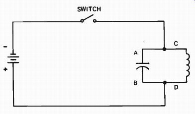
Figure 1. A simple method of producing a damped wave.
DAMPED WAVES
Consider the circuit shown in Fig. 1 . A coil and capacitor are connected in parallel and connected to a battery through a switch. For our discussion we must assume that the switch can be opened and closed instantaneously. Now let's see what happens when we close the switch for an instant.
At the instant the switch is closed, electrons flow from the negative terminal of the battery into side A of the capacitor. At the same instant, electrons will flow out of side B of the capacitor to the positive terminal of the battery. If the resistance in the circuit, which includes the battery resistance, is very low, the capacitor can charge up almost instantly to a voltage equal to the battery voltage. Thus, terminal A of the capacitor will be negative and terminal B will be positive.
At the same time, when the switch is closed, there will be some tendency for current to flow through the coil from terminal C to terminal D. However, you will remember that one of the characteristics of a coil or inductance is that it opposes any rapid change in the current flowing through it. The instant before the switch is closed, the current flowing through the coil is zero. The coil would like to keep it that way. When the switch is closed, the inductance of the coil tries to prevent a current from building up in the coil.
Actually, there will be some small current flowing through the coil from terminal C to terminal D, but if the switch is closed only for an instant, the current will not be able to build up appreciably.
Therefore, at the instant the switch is opened again we have the capacitor charged, as shown in Fig.2(A), and a small current flowing through the coil as indicated.
When the switch is opened and we have the situation shown in Fig.2(A), we have a capacitor that is charged, and immediately starts to discharge. As a result, a current flow will be set up in the circuit as shown in Fig.2(B). Now remember that a coil opposes a change in the current flowing through it. Therefore the capacitor cannot discharge instantly through the coil, but rather must build up a current in the coil which will build up a magnetic field about the coil. Eventually, the capacitor will build up a current flow in the coil and enough electrons will leave plate A to get to plate B to discharge the capacitor.
The discharge of the capacitor removes the voltage that caused current to flow through the coil. The magnetic field around the coil now collapses. The collapsing field generates an emf in the coil, which tends to keep the current flowing in the same direction as before. This continued current causes electrons to flow onto plate B of the capacitor, giving the capacitor a charge opposite to what it had at the start. This condition is shown in Fig.2(C).
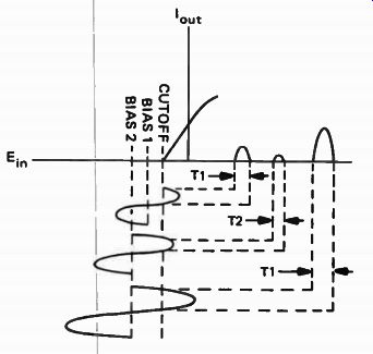
Figure 2. How oscillation takes place in a resonant circuit.
After the field around the coil has collapsed, there is no emf to hold the charge on the capacitor.
The capacitor now begins to discharge back through the coil as shown in Fig.2(D). The flow of current caused by the discharge of the capacitor builds up a magnetic field around the coil until the capacitor is fully discharged; the magnetic field collapses and keeps the current flowing. This current flow charges the capacitor with the same polarity it had at the instant the switch was opened. This is shown in Fig. 2(E). Again, the current will eventually drop to zero, and then the capacitor will once again begin to discharge through the coil in the opposite direction, this time with electrons flowing from plate A to plate B as shown in Fig.2(F). Notice that in Fig.2(F) we have the same situation as we had in Fig.2(B). In other words, we have gone through a complete cycle of events. The capacitor was charged with one polarity. This produced a current flow through the coil, which eventually charged the capacitor with the opposite polarity. The capacitor then began to discharge through the coil in the opposite direction, which built up a charge on it having the same polarity as the original charge placed on the capacitor. Once again this charge on the capacitor began the cycle of events all over again by attempting to discharge through the coil.
You might think that this oscillation, or backward and forward flow of current through the coil to charge and discharge the capacitor, would continue indefinitely. Indeed, if we had a perfect coil and a perfect capacitor, once the oscillation was started, it would continue indefinitely. How ever, there is no such thing as a perfect coil or a perfect capacitor. There will be some losses in both parts, so instead of having an oscillation which continues indefinitely, we will have what is called a damped wave. The damped wave of voltage across the capacitor is shown in Fig.3.
The important thing to notice in this damped wave is that the amplitude of each cycle is just a little bit less than the amplitude of the preceding cycle. In other words, the wave is slowly dying out because of losses in the resonant circuit. The lower the losses in the circuit, the greater the number of cycles that will occur before the wave disappears.
On the other hand, the higher the losses in the circuit, the fewer the number of cycles.
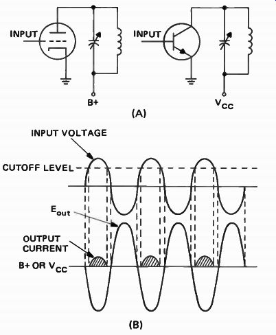
Figure 3. Voltage across the capacitor.
If we could find some way of closing the switch in Fig.1 for just an instant when plate A of the capacitor reaches its maximum negative charge, we could supply a small amount of energy to the resonant circuit to make up for losses in the circuit. If we continue to supply this small amount of energy once each cycle, then the resonant circuit will continue to oscillate indefinitely, and we could use it as a source of ac power. This is what an oscillator does - it supplies a pulse of energy at the correct time to make up for losses in the resonant circuit. We'll see how this is done later, but let's learn more about resonant circuits first.
FACTORS AFFECTING RESONANT CIRCUITS
There are several additional important things we should know about resonant circuits. For example, we should know the frequency at which oscillation takes place in a resonant circuit. We should also know what factors affect the loss of energy from cycle to cycle. In other words, how rapidly the wave train will die out.
Another term that we frequently encounter when dealing with resonant circuits is "period." We will now learn something about these factors.
Frequency. The frequency at which a resonant circuit oscillates will depend upon the inductance and capacitance in the circuit. We already know that resonance occurs when the inductive reactance of the coil is exactly equal to and canceled by the capacitive reactance of the capacitor. In other words, at resonance:
XL = Xc
We know that the inductive reactance of a coil, XL, is given by the formula:
XL =6.28XfXL
and the capacitive reactance of a capacitor is given by the formula:
Xc = 6.28x f x C 1
Now, since resonance occurs when XL = Xc, let's substitute the values for XL and Xc and we will get: XL = Xc 6.28 X f X L -
1 6.28 X fX C and this can be manipulated to give us:
1 f 2 - 6.282 XLXC and now if we take the square root of both sides of the equation we get: f= 1 6.28 X N / L X C
For convenience in expressing formulas of this type, the times sign is usually omitted, and in place of 6.28, the term 27r is often used. You will usually see the formula for the frequency at which a resonant circuit will oscillate expressed as:
1 f - 2 pi Nrr- _,C
You should remember this formula because it is very important; but even more important, remember what the formula tells you. The formula says that the frequency of a resonant circuit varies inversely as the square root of the LC product.
Now remember we mentioned before that when one factor varies directly with another, making one bigger makes the other bigger; and when two factors vary inversely we have the opposite situation: making one bigger makes the other smaller. Here we have a situation where the frequency varies inversely as the square root of the LC product.
This means that increasing the size of either L or C will reduce the frequency at which the resonant circuit oscillates, and reducing the size of either L or C will increase the frequency at which the resonant circuit oscillates. We can express this simply by saying: Larger L or C, lower frequency; smaller L or C, higher frequency.
In using this formula, the frequency of oscillation will be given in cycles per second and the value of L and C used must be in henrys and farads respectively.
Period. The period of a resonant circuit is the time it takes the resonant circuit to go through one complete oscillation. Thus, if we have a circuit that is resonant at a frequency of 1000 cycles per second, its period would be 1/1000 of a second, and if we have a resonant circuit that is resonant at a frequency of 1,000,000 cycles per second, the period would be 1/1,000,000 of a second.
The period of a resonant circuit is given by the formula: where P represents the period of the resonant circuit in seconds and f the frequency in cycles per second.
Since in electronics we are usually dealing with comparatively high frequencies, it follows that the period of most resonant circuits will be only a very small fraction of a second. As a matter of fact, the period of many resonant circuits will be only a small fraction of a millionth of a second. There fore, to simplify things, the microsecond is frequently used in electronics work as a unit of time.
A microsecond is 1/1,000,000 (one-millionth) of a second. Thus, if a resonant circuit has a period of 5/1,000,000 (five-millionths) of a second, we can say that its period is 5 microseconds. Or, if another resonant circuit has a period of 1/10,000,000 (one ten-millionth) of a second, we can say this period is one-tenth of a microsecond.
In order to show the cycle-time relationship, the frequency of a circuit is measured in units called HERTZ. One hertz being equivalent to one complete cycle in one second, 1000 cycles in one second would then be 1000 hertz (Hz) or one kilohertz (kHz). 1,000,000 cycles in one second would be one megahertz (MHz). These terms are replacing the older terms of kilocycles (kc) and megacycles (mc) still used in many publications.
The Q Factor. The number of cycles that will occur when a resonant circuit is shock-excited depends almost directly upon the Q of the coil.
The higher the Q, the more cycles will occur.
The Q of a coil tells us essentially how good a coil we have. A coil that has a high Q has a high inductive reactance compared to the resistance of the coil. A coil with a low Q has high resistance compared with the inductive reactance.
The Q of a coil is expressed by the formula:
XL Q = and we can express XL as equal to:
6.28 X fx L and substituting this in the formula for the Q of a coil we get:
6.28 X fX L Q
If we examine this formula, we see that the Q varies directly as the frequency and inductance and inversely as the resistance. Therefore, you might think that increasing the frequency of the resonant circuit by using a smaller capacitor in conjunction with the coil will result in a higher Q. This will often happen, but the increase in Q is not as great as might be expected, because the resistance of the coil is the ac resistance rather than the dc resistance. The ac resistance of a coil actually represents ac losses in the coil and this varies directly as frequency varies. Therefore, increasing the frequency of the resonant circuit increases the inductive reactance of the coil, but at the same time it increases the losses so that the Q normally does not increase as fast as we might expect.
In a resonant circuit with a high Q coil there will be a large number of cycles in a damped wave train set up by shock-exciting the resonant circuit.
In other words, the amplitude of one cycle will be very little less than the amplitude of the preceding cycle. However, if the Q of the coil is low, then the losses in the coil will be quite high so that the amplitude of each cycle will be substantially less than the amplitude of the preceding cycle. This means that the oscillation will be damped out quite rapidly and the number of cycles that occur when the circuit is shock-excited will be somewhat limited.
In most oscillator circuits a comparatively high Q coil is used. The reason for this is that if the coil has a high Q, then only a small amount of energy must be supplied by the tube or transistor in the oscillator circuit in order to sustain oscillation. On the other hand, if the coil has a low Q, the losses in the resonant circuit will be quite high, with the result that the tube or transistor used in the oscillator circuit must supply a comparatively large amount of energy in order to keep the oscillation going.
SELF-TEST QUESTIONS
1 What type of feedback is used in oscillator circuits?
2 If the inductance of an LC circuit is increased, what happens to the frequency?
3 If the Q of the resonant circuit is increased, what happens to the damped wave train?
4 If the resonant frequency of an LC circuit is 2000 kHz, what is the period of one cycle?
++++++++++++++++++++
The Basic Oscillator
The function of the switch in Fig.1 is to supply energy of the proper phase and at the proper time to sustain oscillations in the resonant circuit. At radio frequencies it would be impossible for a mechanical switch to do this. Therefore, we must use an electronic switch such as a vacuum tube or transistor.
THE ELECTRONIC SWITCH
In order to see how the vacuum tube can be used as an electronic switch, let's go back to the basic circuit we had in Fig. 1. We have repeated this circuit as Fig.4(A). It is exactly the same as Fig.1 except we have simply indicated where the battery voltage is to be connected instead of actually showing the battery in the circuit. In practice, we could use either a battery or the dc output of a suitable power supply. If we can momentarily close the switch, we will charge the capacitor C1 and produce oscillation in the parallel-resonant circuit consisting of C1 and L1. However, this oscillation will die out after a number of cycles because of the losses in a resonant circuit, unless we can find some way of supplying additional energy to the resonant circuit to make up these losses. If we could close the switch at the right instant during each cycle, we could recharge capacitor C1 once each cycle and keep the oscillation going. However, if the resonant frequency of the circuit is several hundred Hz or higher, it would be impossible to close the switch manually at the correct instant to keep the oscillation going. As a matter of fact, it would be difficult to do this mechanically except at a very low frequency.
Figure 4. Using a tube as an electronic switch to supply the losses
in a resonant circuit.
In Fig.4(B), we have replaced the switch with a vacuum tube. The cathode of the vacuum tube is connected to the negative side of the power supply or battery, and the plate of the tube is connected to the resonant circuit. Between the cathode and the grid of the tube, we have connected a battery that will place a negative voltage on the grid of the tube. The battery voltage in the grid circuit is high enough to bias the tube beyond cutoff. Thus, with the circuit exactly as shown in Fig.4(B), the bias on the tube is so high that there will be no current flowing through the tube and hence no way to charge capacitor C1 and start the resonant circuit oscillating. We have in effect the same situation as we have in Fig.4(A) with the switch open.
Now let's look at the circuit shown in Fig.4(C). Here we still have the tube connected in the circuit in exactly the same way except that we have added a coil, L2, between the negative terminal of the grid battery and the grid of the tube. This coil is placed near L1 so that it will be inductively coupled to L1. Thus, if there is any change in the magnetic field about L1, the changing flux will induce a voltage in L2.
Now let's consider what will happen if we momentarily short the plate and cathode of the tube together. If we do this, capacitor C1 will be charged. As soon as we remove the short, C1 will start to discharge through L 1 and in doing so will build up a magnetic field about L1. The changing lines of flux will cut L2 and induce a voltage in it.
This voltage in L2 will be in series with the battery voltage applied between the cathode and grid of the tube. If the end of L2 that connects to the grid of the tube is negative, and the other end positive, then the voltage induced in L2 will add to the grid bias, biasing the grid still further negative so that no current can flow from the cathode to the plate of the tube. However, if the voltage induced in L2 has a polarity such that the end of L2 that is connected to the grid is positive, and the other end is negative, then this voltage will oppose the battery bias voltage and reduce it so that the total grid bias will be reduced below the point where the plate current is cut off, and current can flow through the tube. Therefore, by connecting L2 with the proper polarity, we can arrange the circuit so that when the plate side of capacitor C1 reaches its negative peak, the tube will conduct, and a burst of electrons will flow through the tube, charging C1 still further. Thus, any loss in the charge across C1 due to losses in the resonant circuit will be made up for by the burst of electrons flowing through the tube.
In Fig.5, we have shown a number of sine-wave cycles such as the oscillation that might occur in the L1- C1 resonant circuit. The shaded pulses represent the bursts of current flowing through the tube that will reinforce the oscillation and keep it going. Notice in Fig.5 that the burst of current flowing through the tube occurs at the correct instant to aid the oscillation. Also, notice that the current burst occurs for only a small fraction of a cycle. The current does not flow through the tube during the entire cycle.
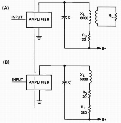
Figure 5. The oscillator pulse is timed to occur at the peak of the
oscillation in the tank circuit to reinforce the oscillation.
For several reasons the oscillator circuit shown in Fig.4(C) is not a practical circuit. For one thing, the battery used to provide the negative bias on the grid is somewhat cumbersome. If we were using a power supply to furnish the voltage to operate this oscillator from a power line, we would not want to be bothered with a separate battery to supply the grid bias. Furthermore, with this type of arrangement, it would be possible to pick up such a high voltage pulse in L2 that the tube would pass an extremely high current when it was driven in a positive direction. As the grid bias battery aged and the voltage from this battery dropped, an even higher current pulse would flow through the tube.
As a matter of fact, the pulse might be so high that the tube could be damaged.
Both of these objections can be overcome by modifying the circuit as shown in Fig.6. Let's look at Fig.6(A) first. In Fig.6(A), you will see that we have replaced the battery in the grid circuit by a resistor, R1, with capacitor C2 connected across it.
In other respects the circuit is identical to the circuit shown in Fig.4(C).
Figure 6. A tuned-plate oscillator.
Let's see exactly how this circuit works. When voltage is first supplied to this circuit, there will be no grid bias on the tube. The tube starts to conduct and charges capacitor C1. Electrons will flow into the side of this capacitor that connects to the plate of the tube and out of the other side. At the same instant, current will start to flow through L1 and there will be a rapid change in the lines of flux about this coil. The changing magnetic lines will cut L2, and induce a rather high voltage in it.
Coil L2 is connected so that the grid of the tube will be driven in a positive direction, which will result in a still further increase in current flowing from the cathode to the plate of the tube, which will charge C I still further.
Since the grid of the tube will be driven in a positive direction, it too will attract electrons, and electrons will flow from the cathode of the tube to the grid, through L2, and then through R1 back to the cathode of the tube. In flowing through R1, they will set up a voltage drop across it and charge capacitor C2 with the polarity indicated on the diagram.
Eventually the rate at which the flux lines are cutting L2 will decrease, so the voltage induced in coil L2 will drop. The voltage across R1 will cut off the flow of plate current in the tube. Capacitor C2 starts to discharge through R1 and keeps the grid of the tube at a high enough negative potential to keep it cut off. When this happens, we have opened the switch as in Fig.1 and an oscillation starts in the tank circuit. The capacitor and coil begin exchanging energy back and forth. At the correct instant, once in each cycle, the grid of the tube will be driven positive by the voltage induced in L2 by the changing flux from L 1 so that the tube will pass a burst of electrons to recharge C1 and make up any energy lost in the tank circuit.
The oscillator we have been discussing is called a tuned-plate oscillator. In actual practice, the circuit is modified and you will usually see it like Fig.6(B). Notice that the position of the grid resistor and grid capacitor, R1 and C2, have been changed with reference to L2. In other words, tracing from the grid of the tube, we come to the grid resistor and grid capacitor first and then through L2 to ground. However, regardless of how the resistor and capacitor are connected in series with L2, the action of the circuit is the same.
This type of oscillator has several disadvantages that can be eliminated by different circuitry.
However, since it is a basic circuit and enables us to see exactly how the tube is acting as a switch, it is a good circuit with which to start our study of oscillators.
SELF-REGULATION
The oscillator circuits shown in Fig.6 are self-regulating. This means that they tend to control the flow of current through the tube themselves. For example, suppose the amplitude of the pulse picked up by L2 should increase for any reason; if this happens, the pulse will drive the grid even more positive than normal. With a higher positive voltage on the grid, a greater number of electrons will be attracted to it. An increase in the number of electrons reaching the grid will mean that more electrons must flow through R1. The voltage developed across R1 depends upon two things: the size of the resistor and the number of electrons flowing through it. Therefore, if the number of electrons flowing through R1 increases, the voltage developed across it will increase.
Notice the polarity of the voltage across R1 . The grid end of this resistor is negative, so this bias voltage tends to reduce the flow of current through the tube. Therefore, the increase in negative voltage across R1 will subtract from the increase of positive voltage across L2 so that the net drive voltage applied to the grid remains almost the same. Thus, even though something might cause the voltage developed in L2 to increase, the tube will compensate for this change by developing an increased bias so that the burst of plate current flowing through the tube will remain essentially constant.
OSCILLATOR-AMPLIFIER
Up to this point, we have been considering the tube as a switch that closed at the proper instant to replenish the losses in the resonant circuit. We can also consider the tube as an amplifier that is amplifying part of its own output. For example, L1 and L2 in Fig.6(B) are inductively coupled together. Part of the output produced across L1 is coupled to L2, where it is fed back into the input circuit. This signal fed into the input circuit is then amplified by the tube and fed to the resonant circuit L1 - C1 in the output. The cycle then continues, with part of the (Kaput being coupled to L2 and once again being fed back to the input.
Thus, the oscillator can indeed be considered as an amplifier that feeds part of its own output signal back to the input, where it is amplified once again.
Of course, the signal fed back to the input must be of the proper phase to sustain oscillation.
The signal must drive the grid in a positive direction when the plate current flowing through the tube should increase. Feedback of this type is called regenerative feedback. In some amplifiers a small amount of regenerative feedback is used to improve the gain of the amplifier. However, in an oscillator, enough regenerative feedback is used to start the stage oscillating, and to keep it oscillating.
OSCILLATOR FREQUENCY
You already know that the resonant frequency, , of a circuit containing L and C is:
f_o = 1 / 2 pi √ (LC)
The resonant frequency is also often expressed in terms of resonant angular frequency, w° :
w° = 1/√ (LC)
where co p = 2 pi X f_o
This expression comes from the fact that there are 2ir radians in 360°. A radian is an angular measurement equal to approximately 57°. Since there are 2 pi radians in 360°, a vector rotating at f. Hz travels through 2 pi X f_o radians per second.
You might at first expect an LC oscillator to operate at exactly co., the resonant frequency of the LC circuit. However, there is always some resistance in the circuit that affects the oscillator frequency. Furthermore, the plate resistance of the tube affects the oscillator frequency so that the actual frequency of the oscillator, co, is:
( co = co o 1 + Rp
where co p is the angular resonant frequency of the LC circuit, R represents the resistance in the resonant circuit, and Rp is the plate resistance of the tube.
In most oscillator stages the value of R will be small, because the Q of the oscillator coil will be high. At the same time, the plate resistance of the tube will be reasonably high so the term R/Rp will be small and co will be almost equal to co.. However, the fact that R and Rp do enter into the frequency means that if either of these values change, the oscillator frequency will change. Thus, oscillator stability depends not only on keeping the values of L and C in the resonant circuit constant, but also the values of R and Rp must be kept constant.
OSCILLATOR STABILITY
One of the most important considerations in oscillator circuits is the stability of the oscillator - in other words, how stable the oscillator frequency is. The output frequency of a radio transmitter is controlled by the oscillator, and if the oscillator frequency does not remain constant, the transmitter output frequency will not be constant.
We have already pointed out that the oscillator frequency depends not only upon the inductance and capacitance in the resonant circuit, but also on other factors such as the resistance of the oscillator coil and the plate resistance of the oscillator tube.
Now, let us consider each of these factors to see exactly what effect each has on the oscillator frequency.
Tank Inductance and Capacitance. The inductance in the oscillator tank circuit is made up of the inductance of the oscillator coil, plus any stray inductance in the circuit. The capacitance in the oscillator tank circuit is made up of the capacity connected across the oscillator coil plus any tube capacity that may be in parallel with the coil and capacitor, and the distributed wiring capacity in the circuit. The inductance in the circuit consists of the oscillator coil, the inductance of the leads connecting the coil to the tube and other parts in the circuit, and any inductance that other parts in the circuit may have. The capacity in the circuit consists of the capacity of the variable capacitor across the oscillator coil, the input capacitance of the tube, the stray wiring capacity in the circuit, plus any stray capacity the coil may have. This total inductance plus this total capacity are the major factors that determine the oscillator frequency.
When an oscillator is first turned on, the values of the inductance and capacitance in the tank circuit will usually change as the tube and other parts in the circuit heat. Therefore, the oscillator stability is usually measured in terms of the oscillator's ability to maintain a constant frequency after enough time has been allowed for the tube and parts to reach normal operating temperature. It is common practice in some transmitters to leave the oscillator on at all times to avoid any frequency drift during the warmup period. In some transmitters, the oscillator coil and capacitor are placed in an oven that is kept at a constant temperature by a thermostatically controlled heater to minimize changes in inductance and capacity due to temperature changes. In some oscillators, special temperature compensating capacitors are connected across the oscillator tank circuit to minimize frequency drift due to tempera ture changes. These capacitors usually have a negative temperature coefficient. This means that their capacity decreases as the temperature in creases. By using a capacitor of this type with the correct temperature coefficient, it is possible to compensate for any increase in inductance or capacitance in other parts in the circuit as the temperature increases.
Changing a tube in the oscillator circuit can result in a change in oscillator frequency. The input capacity of the tube used in the oscillator circuit makes up part of the oscillator tank circuit.
The input capacity of different tubes of the same type may vary appreciably, so putting a new tube in this or any other oscillator circuit may change the tank circuit capacitance, and hence the frequency. Therefore, if you replace the oscillator tube in a transmitter you should check the output frequency.
Tank Losses. Earlier we pointed out that the angular resonant frequency, w., of the oscillator tank circuit is given by: 1 w 0 = and at the same time, the actual frequency at which the oscillator oscillates is given by: R w = w. (1 + - Rp where R is the resistance in the tank circuit and Rp the plate resistance of the tube.
The term R represents the ac resistance of the tank circuit, and as such represents all the losses in the tank circuit. Thus, this term includes such factors as coil resistance and losses from the oscillator circuit due to loading of the circuit.
Therefore, any change in the oscillator coil resistance will result in a change in oscillator frequency.
Similarly, a change in the loading on the oscillator will result in a change in oscillator frequency.
Thus, for maximum stability, the oscillator should be lightly loaded and the load on the oscillator must remain constant.
The Plate Resistance. Since the plate resistance of the tube enters into the frequency of the oscillator, any change in plate resistance will produce a change in the oscillator frequency. The plate resistance of the tube will change if either the plate or grid voltage is changed in the case of a triode, and if the grid or screen voltage (and to some extent the plate voltage) is changed in the case of a pentode. Thus, it is important that the voltages supplying the oscillator be kept constant.
These voltages must also be free of hum, which actually is a changing voltage superimposed on the dc supply voltage, because the hum voltage could produce a constantly changing plate resistance which will result in a frequency-modulated signal being generated by the oscillator.
Changes in loading on the oscillator may affect the bias developed on the grid of the tube. When this happens, the grid voltage will change, causing the plate resistance and hence the frequency to shift.
Looking at the expression for the oscillator angular frequency, we see that the frequency is equal to the angular frequency of the tank circuit times one plus a fraction. Thus, the oscillator frequency will be higher than the resonant frequency of the tank circuit. Also, if the term R/Rp is small, which it usually is, the oscillator frequency will differ from the tank frequency by only a small percentage. However, at high frequencies, this small percentage or fraction can represent a great enough frequency change to cause concern.
For example, if the resonant frequency of a tank circuit is 10 MHz and the value of R/Rp is only 0.01, 0.01 X 10,000 kHz represents 100 kHz so the oscillator frequency would be 10,100 kHz, or 10.1 MHz. If the value of Rp changed because of changing voltages on the tube, the oscillator might drift 50 kHz or more above or below this frequency.
TRANSISTOR OSCILLATORS
Of the three basic transistor configurations, the common emitter is the most frequently used in rf oscillator circuits. There are several reasons for this. The power, current, and voltage gains of the common-emitter configuration are all greater than one, and the highest possible power gain can be had. Also in the common-emitter circuit, moderate input and output impedances make less power necessary for feedback. In the common-base con figuration, low input and high output impedances inherent in the circuit cause a mismatch in the feedback circuit, producing greater losses and requiring more feedback. The current gain in the common-base circuit is less than one, even though voltage and power gains are greater than unity. A somewhat similar condition exists in a common collector circuit where high input and moderate output impedances exist. Voltage gain is less than unity, but current and power gains are greater than one.
Transistor oscillators may be designed to operate class A, B, or C depending on the desired efficiency. Since rf oscillators are also amplifiers, bias supply and temperature stabilization are similar to rf amplifiers discussed in a previous lesson.
A combined voltage divider and feedback type biasing arrangement is often used because it helps produce oscillation and at the same time establishes a stable dc bias point. Emitter biasing with a bypass capacitor is also used, the operation being similar to grid leak biasing. Usually the amplitude is regulated by driving the transistor into saturation or by using special diode limiting circuits. Either shunt or series type collector feed may be used, the shunt type being preferred for greater output efficiency.
Frequency stability of the transistor oscillator is equivalent to, and sometimes greater than, the electron tube oscillator. The use of lower voltages, currents, and power permits construction of better tank circuits. In particular, the low power used with transistors aids in stability due to the decrease in heat. One major disadvantage of transistors is their critical operating point. A slight bias change can cause a large shift in frequency.
The collector-to-emitter capacitance of the transistor also affects frequency stability. This internal capacitance will vary with changes in collector or emitter voltages and with temperature.
In high-frequency oscillators it is sometimes necessary to place a swamping capacitor across the collector to emitter leads. The total capacitance of the two in parallel results in a circuit which is less sensitive to voltage changes. The added capacitor may be a part of the tuned circuit.
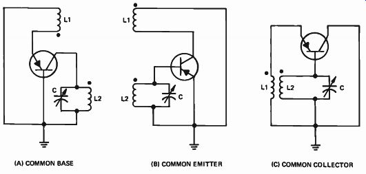
Figure 7. Tickler coil oscillators.
Partial compensation of voltage changes may be obtained by use of a common supply. Since an increase in collector voltage tends to increase oscillator frequency and an increase in emitter voltage decreases oscillator frequency, the use of a common bias source for both the collector and emitter helps stabilize the frequency. By using a common bias source, a change in one is somewhat counteracted by the change in the other.
The three basic transfigurations used for oscillators are shown in Fig.7. Bias and feed arrangements are omitted for simplification. Although any of the basic transistor configurations can be used, generally only two, the common emitter and common-base, are used in actual practice. The common-emitter configuration offers the advantages of easily matched input and output impedances and its close parallel to the electron tube.
The major advantage of the common-base circuit is that at high frequencies collector-emitter capacitance helps feed back an in-phase voltage independently of tickler coil L1, and oscillation is more easily obtained. In the common-emitter circuit, this capacitance feeds back an out-of-phase voltage which requires additional feedback from the tickler coil to overcome it. In both the common-base and common-emitter circuits, oscillation is easily sustained. This is the result of feedback provided by voltage induced through the mutual inductance of L1 and L2. In the common collector circuit, the voltage gain is always less than unity; therefore, feedback tends to be insufficient for stable oscillations at the lower frequencies. At the higher frequencies it is assisted by the base emitter capacitance. Sometimes, an external capacitor is added between the base and emitter to give additional feedback.
Operation of the LC circuit is similar to that of the electron tube circuit. As the oscillator is switched on, current flows through the transistor as determined by the biasing circuit. Initial current produces a feedback voltage between the collector and the emitter which is in-phase with the input circuit. As emitter current increases, collector current increases and additional feedback between L1 and L2 causes the emitter current to increase until saturation is reached. When saturation is reached, emitter current is no longer changing (increasing), and the induced feedback voltage is therefore reduced. At this time the collapsing field around the tank and tickler coils induces a reverse voltage into the emitter circuit which causes a decrease in the emitter current, thus causing a decreasing collector current. The decreasing cur rent then induces a greater reverse voltage in the feedback loop driving the emitter current toward cutoff.
Although the emitter is cut off, a small reverse (leakage) current flows. This current has no effect on the operation of the circuit but it does represent a loss which lowers the efficiency. In this respect the transistor differs from the electron tube, which has zero current at cutoff.
The discharge of the tank capacitor through L2 will cause the voltage applied to the emitter to rise from a reverse bias to a forward bias condition.
Emitter and collector current start to increase and the cycle repeats itself.
The transistor oscillator circuit that most closely resembles the tuned-plate vacuum tube oscillator is the tuned-collector oscillator. This circuit is shown in Fig.8.
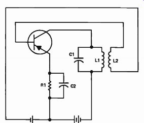
Figure 8. A tuned-collector oscillator.
Notice that in this circuit the resonant circuit consisting of C1 -L1 is in the collector circuit of the transistor. L2 is inductively coupled to LI so energy is fed from L1 to L2. The signal developed in L2 is fed back to the base of the transistor.
In the operation of this oscillator, resistor R1 and capacitor C2 develop a bias voltage sufficient to cut off the transistor. The signal needed to overcome this cutoff bias is induced in L2 and applied between the base and the emitter. Since this is a pnp transistor, the signal in L2 must make the base negative and the emitter positive at the instant that a pulse of current is needed from the collector in order to sustain oscillation in the resonant circuit consisting of L I and C1.
SELF-TEST QUESTIONS
5. Describe the phase relationship between the plate current wave shape and the voltage wave shape developed across L2 in Fig.4(C).
6. What makes the oscillator in Fig.6(B) self regulating in regard to the amplitude of the grid signal?
7. List three means of reducing frequency drift due to changes in temperature in a resonant circuit.
8. In high-frequency transistor oscillators, what is sometimes used to compensate for collector to-emitter capacitance?
9. In the oscillator circuit in Fig.8, where is the bias developed and what component develops the signal that overcomes this bias?
++++++++++++++++++++++++++
Practical Oscillator Circuits
The oscillator circuits we have discussed up to this point weren't very practical. They were used to illustrate some of the basic characteristics of oscillators. Let us now look at some practical circuits actually found in communication equipment. These oscillators are grouped according to the type of resonant circuit used, inductance capacitance (LC) or resistance-capacitance (RC).
LC OSCILLATORS
The LC oscillators can be placed into one of two classifications: those using inductive feedback and those using capacitive feedback. The inductive feedback oscillator uses inductive coupling to return a portion of the output back to the input.
The capacitive feedback circuit uses capacitive coupling to accomplish this. Although there is some difference in the circuitry involved, both types are LC oscillators, and the net result is essentially the same.
OSCILLATORS USING INDUCTIVE FEEDBACK
One of the most important and most widely used oscillators in electronics work is the Hartley oscillator. This oscillator uses inductive feedback.
The resonant circuit is placed in the grid circuit of the tube or the base circuit of the transistor instead of in the output circuit as in the case of the tuned-plate and tuned-collector oscillators. How ever, before we look at the Hartley oscillator let's look at another oscillator which will help you understand how the Hartley oscillator works. Let's first look at the tuned-grid oscillator.
Tuned-Grid Oscillator. Two versions of the tuned-grid oscillator are shown in Fig.9. The circuits are basically the same; the only electrical difference is in the connection of the grid resistor R1. In the circuit shown in Fig.9(A), R1 is connected directly across the grid capacitor C2, whereas in the circuit shown in Fig.9(B), R1 is connected between the grid and the cathode of the tube. The action of R1 is the same in both cases; it provides a path for the electrons striking the grid of the tube to get back to ground or the cathode of the tube. In the circuit of Fig.9(A), when C2 discharges through R1 to develop negative bias for the tube, there is no discharge through the tank circuit. In Fig.9(B), when C2 discharges through R1, the discharge current also flows through the tank circuit.
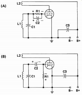
Figure 9. Two versions of the tuned-grid oscillator.
Actually, the biggest difference between this oscillator and the tuned-plate oscillator that you already studied is that the resonant circuit is in the grid circuit instead of the plate circuit. With this circuit, when the power is turned on, changes in plate current will set up a changing magnetic field about L2. L2 is inductively coupled to L1 so the changing magnetic field about L2 will induce a voltage in L1. The induced voltage charges capacitor C1, starting the oscillatory discharge in the tank circuit consisting of L1-C1. The voltage across C1 becomes the grid voltage because the value of C2 is large enough so that its reactance is so small at the frequency of oscillation, that the grid is, in effect, connected directly to C1.
Now since the increasing plate current causes the end of C1 that is connected to the grid through C2 to swing in a positive direction, the grid of the tube is driven in a positive direction. Driving the grid positive produces two effects; it increases the plate current, causing C1, and hence the grid, to be driven still further in a positive direction, and it causes grid current to flow, which charges C2 with the polarity shown on the diagram.
Now if the plate current of the tube could keep on increasing indefinitely, the grid end of C1 would be driven more and more positive. However, there is a limit to how high the plate current can become, because a balance will be reached between the positive voltage across C1 and the negative voltage across C2. When this happens, the plate current flowing through L2 will no longer change.
We will no longer have voltage induced in L1, and C1 will begin to discharge through L1, setting up an oscillation in the LC circuit. As soon as this happens, the positive voltage on the grid end of C1 begins to disappear, and the plate current will be cut off by the negative voltage across C2. The LC circuit is now free to oscillate as though the tube were removed from the circuit. C2 meanwhile starts to discharge through R1, setting up the voltage drop across it as shown on the diagram.
During the next half cycle when the voltage on the grid end of C1 again becomes positive, it will drive the grid in a positive direction enough to let some plate current flow through the tube; this will result in a change in the field about L2 which will induce a voltage in L1 which drives the capacitor and the grid voltage still further in a positive direction.
The important point to remember about this oscillator is that the energy needed to sustain the oscillation in the tank circuit, consisting of L 1 and C1, is inductively coupled to L1 from L2. This energy comes from the plate of the tube in the form of bursts of plate current which produce a changing magnetic field about L2. These bursts of current are the result of the grid of the tube being driven positive by the voltage across C1 swinging positive once each cycle.
The Hartley Oscillator. Two Hartley oscillators are shown in Fig.10. The circuit shown in Fig.10(A) uses a vacuum tube, whereas the one shown in Fig.10(B) uses a transistor. Although the operation of the two circuits is so similar that if you understand one, you will understand the other, we will go through both circuits in consider able detail.
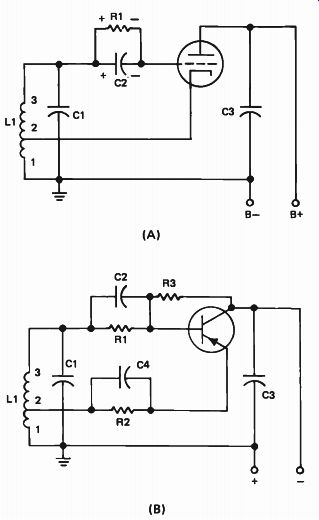
Figure 10. Typical Hartley oscillators; a vacuum tube Hartley oscillator
is shown at (A), and a transistorized one at (B).
Notice the difference between the Hartley oscillators and the tuned-grid oscillators. The tuned-grid oscillator has two coils, whereas the Hartley oscillator uses only a single tapped coil. In the circuit shown in Fig.10(A), the cathode of the tube is connected to the tap, and in the circuit shown in Fig.10(B), the emitter of the transistor is connected to the tap.
In the circuit shown in Fig.10(A), when the plate current starts to flow through the tube, current must flow through the lower half of the coil between terminals 1 and 2. Since the entire coil is wound on a single form, all the various turns of the coil are inductively coupled together.
Therefore the increasing plate current flowing between terminals 1 and 2 will produce a changing magnetic field which will induce a voltage in the portion of the coil between terminals 2 and 3. This voltage will charge capacitor C1 with the polarity such that the end of the capacitor that connects to the junction of C2 and R1 is positive. Again since the value of C2 is chosen so that its reactance is practically zero at the oscillation frequency, the grid of the tube is in effect connected directly to C1. This means that the increase in plate current will drive the grid of the tube in a positive direction, causing a still stronger burst of current through the coil. This in turn causes still higher induced voltage between terminals 2 and 3 which again charges capacitor C1 still further. At the same time when the grid is driven positive, it will attract electrons, and C2 will be charged with the polarity shown.
As in the tuned-grid oscillator, the point is eventually reached where there is a balance between the positive voltage applied to the grid by C1 and the negative voltage applied to the grid across C2 and R1 so that there is no further increase in plate current. This means that the magnetic field produced by the current flowing between terminals 1 and 2 becomes constant and no further voltage will be induced in the coil. C1 starts to discharge through the coil, and the oscillating cycle is started. Furthermore, the positive voltage on the end of C1 that connects to the grid of the tube through C2 disappears, and the tube stops conducting.
Again, the tube will be biased beyond cutoff by the discharge of C2 through R1. These electrons charge C2 during the portion of the cycle when the grid is conducting. When grid current stops flowing, C2 will discharge through R1, setting up a voltage drop across it such that the grid end is negative. This voltage across R1 maintains the bias on the grid of the oscillator tube.
In some cases you will see slight variations of the Hartley oscillator circuit. In some instances, R1 may be connected between the grid and cathode or from the grid of the tube directly to ground. In another variation the cathode connects directly to ground, R1 connects between the grid of the tube and ground, and then the plate of the tube connects directly back to terminal 1 of the oscillator coil. The B+ voltage is then applied to terminal 2 of the coil. This is simply a modification of the Hartley oscillator circuit; it works in exactly the same way as the Hartley oscillator shown in Fig. 10(A). In the circuit shown in Fig.10(B) we have a pnp transistor. When holes begin to travel from the emitter to the collector, electrons will flow from the emitter through R2 to terminal 2 on the coil.
From terminal 2 they will flow through the coil to terminal 1 and back to the positive terminal of the battery. The electrons, in flowing through the coil from terminal 2 to terminal 1, will build up a field about this part of the coil. This field will be a changing field as the current builds up, and this will induce a voltage in the portion of the coil between terminals 2 and 3. The induced voltage will charge C1 with the polarity such that the end connecting to terminal 3 of the coil is negative and the other end is positive. This negative voltage on one end of C1 will be applied to the base of the transistor through capacitor C2 because C2 has a low reactance at the frequency of oscillation. The negative voltage on the base of the transistor will increase the forward bias across the emitter-base junction, causing an increase in the number of holes flowing from the emitter to the collector.
This causes a still further increase in the electron movement from terminal 2 to terminal 1 of the coil, causing the base of the transistor to be driven still further in a negative direction.
In this circuit when the number of holes flowing from the emitter to the collector increases, terminal 3 of the coil will be driven in a negative direction, and when the holes flowing from the emitter to the collector decrease, terminal 3 will be driven in a positive direction. Remember that in a pnp transistor, driving the base in a negative direction causes the holes moving through the transistor to increase, whereas driving it in a positive direction causes the number of holes flowing from the emitter to the collector to decrease. The burst of hole movement through the transistor causes the electron movement from terminal 2 to terminal 1 of coil L1 to flow through the coil in burst, and this burst of energy makes up for any losses in the resonant circuit consisting of L1 and C1.
It is interesting to note the similarity between the circuits shown in Fig.10(A) and Fig.10(B). Although we have a vacuum tube used in one circuit and a transistor in the other, there is a great deal of similarity between the two circuits and the way they work. In each case we have energy lost in the resonant circuit being replaced by bursts of energy; from the tube in one case and from the transistor in the other case. Also notice that the energy is fed across only part of the coil in each case, but the voltage induced in the entire coil is enough to set up a current flow that will replace the capacitor charge that is lost because of resistance or other losses in the resonant circuit.
OSCILLATORS USING CAPACITIVE FEEDBACK
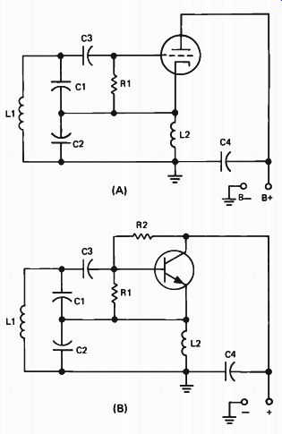
Figure 11. Two Colpitts oscillators.
There are a number of different oscillator circuits in which capacitive feedback rather than inductive feedback (as in the preceding examples)
is used to sustain oscillation. Let's look at some of them now.
Colpitts Oscillator. Perhaps the most important of the oscillators using capacitive feedback is the Colpitts oscillator shown in Fig. 11. The one in Fig.11(A) uses a vacuum tube while the one in Fig.11(B) uses a transistor.
The operation of the two oscillators is quite similar. When the equipment is first turned on, current flows through L2, which is the small rf choke used to complete the cathode circuit in Fig.11(A) and the emitter circuit in Fig.11(B). Current flowing through the coil produces a voltage drop across the coil, and this charges capacitor C2. The charge on capacitor C2 will start an oscillation in the tank circuit, which consists of coil L 1 and two capacitors, C1 and C2. Remember that when we have two capacitors connected in series they will act like one capacitor insofar as the coil is concerned, and the circuit will start to oscillate. The voltage developed across C1 is the feedback voltage. It is applied between the grid and the cathode in the circuit shown in (A) and between the emitter and the base of the circuit shown in (B). When this voltage swings in a direction that makes the end of C1 connected to C3 positive and the other end negative, it will increase the current flowing through the tube or transistor, causing an increase in current flow through L2, which charges C2 still further. When the polarity of the voltage across CI reverses, the voltage will oppose the current flow and in Fig.11(A) simply add to the bias between the grid and the cathode, reducing the plate current to zero; or in Fig.11(B), put a reverse bias across the emitter-base junction, reducing the current flowing through the transistor to practically zero.
The amount of feedback voltage applied to the input of the circuit depends upon the ratio of C1 to C2. If C1 is large compared to C2, the reactance of CI will be low and the reactance of C2 will be high. Most of the voltage developed across the capacitors will be developed across the higher reactance, in this case C2. This means that the feedback voltage applied to the input will be low.
However, if C1 is small compared to C2, the reactance of C1 will be high compared to the reactance of C2 and the feedback voltage supplied to the input of the circuit will be high.
The ratio of C1 and C2 can be altered to provide the required feedback to the input circuit to sustain oscillation. If the value of C1 is increased and the value of C2 decreased by the correct amount, the total capacity in the circuit formed as the result of two capacitors in series remains the same, and hence the resonant frequency of the oscillator does not change.
In some Colpitts oscillators an additional capacitor is connected directly across L1. This is done to provide some means of changing the resonant frequency so we can vary the frequency at which the oscillator oscillates. It is impractical to try to vary both C1 and C2 at the same time, but an additional capacitor placed directly across the coil can be varied, and this will change the resonant frequency of the oscillator. At the same time, since C1 and C2 will still form a voltage divider, part of the total voltage developed across the two capacitors in series is fed back to the input circuit; this part can still be controlled by the proper selection of C1 and C2.
There are a number of variations of the Colpitts oscillator circuit. It is sometimes found in radio transmitting equipment that must be de signed so that its frequency can be varied. The Colpitts oscillator can be designed with excellent frequency stability. By this we mean that once the oscillator is adjusted to operate at a certain frequency, it will not drift from that frequency very much. Some oscillators, on the other hand, do not have good frequency stability and will drift appreciably.
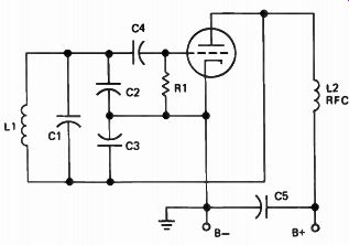
Figure 12. A variation of the Colpitts oscillator.
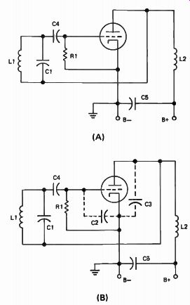
Figure 13. The ultra-audion oscillator.
Another variation of the Colpitts oscillator circuit is shown in Fig.12. Here we have the capacitor C1 connected across L1 in addition to the voltage divider capacitors C2 and C3.
Notice that in this circuit the plate of the tube is fed back directly to L1, C1, and C3 and that the choke coil L2 has been moved from the cathode circuit to the plate circuit of the tube. The cathode in this oscillator circuit is connected directly to ground.
In this oscillator, when the plate current in creases there will be a voltage developed across the rf choke, L2, in the plate circuit of the tube, and this voltage will charge C3. Once this capacitor is charged, oscillation starts in the circuit just as in the Colpitts oscillators shown in Fig.11.
The Ultra-Audion Oscillator. Another oscillator that uses capacitive feedback is the ultra-audion oscillator shown in Fig.13(A). When this type of oscillator was first developed, it was considered as a new type of oscillator. However, with careful analysis, we can see that it is actually a Colpitts oscillator, practically identical to the oscillator shown in Fig.12. We have used the same designations to identify the parts in the circuits shown in Figs.12 and 13. As you can see, the parts are all the same except for C2 and C3, which Fig.13(A) does not seem to have. However, in Fig.13(B) we have shown these two capacitors. C2 is the grid-to cathode capacity of the tube, and C3 is the plate-to-cathode capacity of the tube. When we consider these two capacities, we have a capacitive voltage-divider network just like the one in Fig.11.
C2 in Fig.1 3(B) is between the grid and the cathode of the tube. Notice that C2 in Fig.12 also is in effect connected between the grid and the cathode of the tube. C2 and C3 are in series in both circuits and they are connected across the tank circuit. C3 connects directly to the lead going from the plate of the tube to one side of the resonant circuit, and C2 connects through capacitor C4 to the resonant circuit. Therefore, this oscillator is simply another form of a Colpitts oscillator.
This type of circuit is frequently used in the vhf oscillators in the tuners of television receivers.
Of course, it is usually shown in the schematic in the form shown in Fig.13(A). Manufacturers seldom draw in the distributed capacities; they expect the technician to know enough about oscillator circuits to recognize this as the ultra-audion oscillator and to know that this is simply a modified form of a Colpitts oscillator.
The Electron-Coupled Oscillator. So far all of the vacuum tube oscillators we have discussed have been triode oscillators. These oscillators are widely used in receiving equipment and are sometimes found in transmitters and other rf power generating equipment. However, they have some disadvantages, one of which is the direct coupling between the output and input circuits through the grid-to-plate capacity of the tube. Loading the output circuit of the oscillator has an effect on the input circuit and hence often results in an appreciable shift in the frequency at which the oscillator is oscillating. The net result is that triode oscillators are not stable enough for some purposes.
An oscillator that overcomes this difficulty is the electron-coupled oscillator. In this circuit a tetrode or a pentode tube is used so that the only coupling between the input and output circuits is in the electron stream flowing from the cathode to the plate of the tube. Schematic diagrams of two electron-coupled oscillators are shown in Fig.14.
The circuit shown in Fig.14(A) is for an electron coupled Hartley oscillator and the one shown in Fig.14(B) is for an electron-coupled Colpitts oscillator.
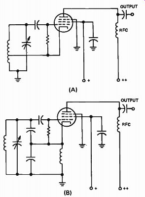
Figure 14. Electron-coupled oscillators; the circuit at (A) is a Hartley
oscillator.
The operation of these oscillators is similar to the operation of the triode oscillators, except that in the electron-coupled oscillator the screen grid of the tube acts like the plate of a triode tube. In other words, insofar as the oscillator action is concerned, we have three elements in the tube to be concerned about, the cathode, the grid, and the screen grid. The screen grid acts like the plate of the oscillator tube. The oscillation is set up in this circuit by these three tube elements. However, the electron stream flows from the cathode of the tube to the plate of the tube, and it is controlled by the grid. Since the grid is biased beyond cutoff during most of the rf cycle, but receives a strong positive pulse during a portion of the cycle, the plate current flowing through the tube flows in the form of pulses, which flow only when the grid of the tube is driven in a positive direction.
In the plate circuit of both oscillators we have shown an rf choke and a capacitor through which the oscillator can be coupled to the following stage. In some electron-coupled oscillators you will find a resonant circuit in the plate circuit of the tube instead of the rf chokes shown in Fig. 14.
In some oscillators, this resonant circuit will be tuned to the same frequency as the resonant circuit in the grid circuit of the oscillator, but in other oscillators you'll find that it is tuned to a frequency equal to twice or three times the frequency to which the resonant circuit in the grid circuit of the tube is tuned. If we tune the resonant circuit in the plate circuit of the tube to twice the frequency of the resonant circuit in the grid circuit of the tube, we will have a frequency doubler.
The resonant circuit in the plate circuit of the tube is set into oscillation by the burst of plate current flowing through the tube. However, since the resonant frequency of this circuit is twice the resonant frequency of the input circuit, the circuit in the plate circuit begins to oscillate at a frequency equal to twice the frequency being generated in the grid circuit. The oscillation in the plate circuit therefore goes through two complete cycles before a second pulse is received from the plate of the tube. This is called a frequency-doubler circuit.
If the resonant circuit in the plate circuit is tuned to three times the frequency of the input circuit, the oscillation set up in the plate circuit will go through three complete cycles before it receives an additional pulse from the plate of the tube. This is called a frequency tripler. You might expect this to result in a damped wave, with the amplitude of the cycles which do not receive a reinforcing pulse from the plate of the tube being considerably less than the amplitude of the particular cycles during which the pulse is received.
Of course, there will be some loss in the resonant circuit and there will be some change in amplitude.
However, by the use of a high Q resonant circuit in the plate circuit, the change in amplitude that occurs each cycle is very small and for all practical purposes all the cycles of the sine wave produced in the resonant circuit will have essentially the same amplitude.
Figure 15. Phase shift oscillators.
RC OSCILLATORS
Resistance-capacitance (RC) oscillators use the charging and discharging action of a capacitor and a resistor in the feedback path to cause oscillation.
The RC oscillator is used in audio and low rf ranges. They offer an inexpensive method of obtaining a fairly stable sine wave within the range of their operation. Although many variations of the RC oscillators exist, there are only two basic types, the phase shift and the bridge.
The phase shift uses a series of RC phase shifting circuits between the output and the input to produce a feedback in-phase with the input. The bridge circuit usually uses an additional tube or transistor to obtain the phase shift and a bridge type circuit to control the feedback at the proper frequency.
Phase Shift. The phase shift oscillators in Fig.15 consist of a conventional amplifier and a phase shift feedback circuit. As in LC oscillators, the feedback must be positive. In the circuits in Fig.15(A) and (B), the output signal will be 180° out-of-phase with the input signal. Therefore the phase shift network must shift the phase of the feedback signal 180°. This phase shift is provided by C1, C2, C3, and R1, R2, R3. One section, C1-R1, of the feedback loop is shown separately in Fig.1 5(C). The impedance of the circuits is capacitive and the feedback voltage, e f, produces a current, i, through CI- R1 which leads e f. The angle of the current lead is determined by the ratio of the reactance of C1 to the resistance R1. As the value of R1 is reduced, the circuit will become more capacitive and more current will lead the voltage up to a maximum of 90°. If resistance is increased the current lead will decrease.
By increasing the number of RC networks, the losses of the total feedback circuit will decrease and a less amount of phase shift will occur in each section of the feedback loop. For this reason some oscillators use five or six RC sections. In Fig.15 each section produces a 60° phase shift. The reactance of the capacitors is inversely proportional to the frequency; therefore, only one frequency will pass through the feedback loop.
Normally the output is fixed in frequency due to the constant value of the capacitors. A variable output may be obtained by using ganged variable capacitors or resistors since an increase in the value of either R or C will decrease the frequency.
Let us examine the operation of the circuit in Fig.15(B). R3 and R4 establish the base bias while R5 and C4 furnish thermal stabilization and furnish an rf ground to the emitter. R6 is the load across which the output is taken and C5 is the coupling capacitor.
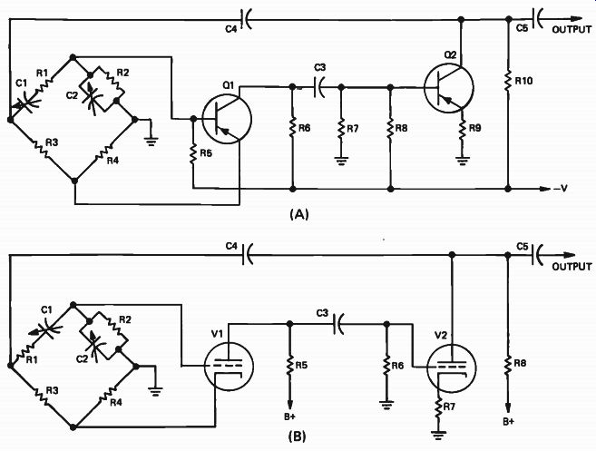
Figure 16. Wien bridge oscillators.
Once power is supplied, operation is started by any random noise in the power source or the transistor. This noise causes a change in base current which causes a large change in collector current. This change in collector current develops an output voltage across R6 which is 180° out-of phase with the original change in base voltage. Part of the signal developed across R6 is returned to the base shifted 180° by the RC network. The shift in phase through the RC network causes the feedback to aid the output, resulting in positive feedback.
With fixed values of R and C, the 180° phase shift occurs at only one frequency; therefore, the output is a sine wave of fixed frequency. At all other frequencies, the reactance either increases or decreases, causing a variation in the phase relationship resulting in degenerative feedback.
The Bridge Oscillator. The Wien bridge oscillators shown in Fig.16 consist of low gain amplifier stages and a resistive-capacitive bridge circuit. The feedback is taken from the second amplifier and returned to the bridge circuit. Since there are two 180° phase shifts between the input of the first amplifier and the output of the second amplifier, the feedback will be positive. The resistive-reactive bridge circuit is designed to be balanced at the operating frequency; therefore, only feedback of the desired frequency reaches the input of the first stage. Let's examine Fig.16(A) and see how this works.
The voltage divider, R2 and R5, supplies base bias for Q1 and R7, and R8 furnishes bias for Q2.
Thermal stabilization is provided by R4 and R9.
R3 and R4 form a resistive leg of the bridge which is in shunt with the output of Q2. A portion of this output coupled by C4 and R3 appears across R4 as negative feedback. Since R4 is not frequency sensitive, the negative feedback is constant regard less of the frequency of the output. At frequencies other than the operating frequency, the negative feedback furnished by R4 will prevent oscillation.
At the frequency of operation, which is controlled by the bridge reactive leg of R1-C1 and R2-C2, the positive feedback to the base of Q1 is maximum.
This in-phase feedback signal is applied to the base of Q1 and is of sufficient amplitude to overcome the negative feedback across R4. The total feed back is therefore positive at the operating frequency.
The amplified output of Q1 is coupled to the base of Q2 by C3 and R7. Q2 further amplifies the signal and the voltage developed across R10 is coupled to the output by CS, and a feedback signal is coupled through C4 to Q1.
We have not covered all of the various LC and RC oscillator circuits you are likely to encounter.
There are many different variations of the circuits we have discussed, and some entirely different circuits. However, most of the circuits you are likely to encounter will be one of the circuits we have discussed in this section of the lesson or a variation of one of these circuits. If you come across a circuit you do not recognize immediately, first determine whether it is RC or LC and, in the latter case, whether capacitive or inductive feed back is used. Once you have decided on the type of feedback that is used, you should be able to figure out how the oscillator circuit works if you keep in mind that its operation is similar to one oscillator we have described in this lesson.
SELF-TEST QUESTIONS
10 When plate current increases in the tuned grid oscillator [Fig.9(B)], what happens to the voltage at the junction of R1 and C2?
11 Where is the feedback voltage developed in the Colpitts oscillator [Fig.11(B)]?
12 The ultra-audion oscillator is modification of what type oscillator?
13 How is the 180° phase shift in feedback voltage accomplished in the phase shift oscillator?
14 What component(s) develops the feedback voltage in the Wien bridge oscillator (Fig.16)?
+++++++++++++++++++++++++
Crystal Oscillators
Although LC oscillator circuits have been developed that have very good frequency stability characteristics, the master oscillators in most transmitters still use crystals. Better frequency stability is the main reason for using crystals instead of LC resonant circuits in master oscillators. The frequency tolerance allowed by the FCC for most transmitting services is very small. The tolerance of a transmitter operating in the broadcast band, for example, is a frequency deviation of only 20 Hz from the assigned frequency. Some services are permitted slightly more frequency tolerance, but in all cases, the tolerance is rather strict. This restriction is necessary to keep the large number of stations operating in the frequency spectrum from interfering with each other.
Several types of materials can be used for crystals. These include quartz, Rochelle salts, and tourmaline. The most often used crystal material for generating radio frequency signals is quartz.
Rochelle salts work better in low-frequency applications, such as in loudspeakers and microphones.
Tourmaline will work as well as quartz, but because it is a semiprecious stone, it is more expensive.
The assembly usually referred to as a crystal is composed of a small piece of crystal material mounted in a holder. The crystal material is in the form of a small slab or wafer cut from a larger crystal. The way in which the wafer is cut from the natural crystal determines many of its electrical characteristics. In this section, we will find out how the crystal works, how the crystal is used in oscillator circuits, and finally we will discuss some of the most-used crystal oscillator circuits.
THE PIEZOELECTRIC EFFECT
A quartz crystal exhibits a property called the piezoelectric (pronounced pi-ee-zo) effect when it is compressed mechanically or when a current is applied to it. To illustrate this effect, suppose we have a small crystal wafer with leads attached to its two surfaces. If we squeeze the wafer or bend it in some way, a voltage will appear between the leads.
If, on the other hand, we apply a small voltage across the leads, the crystal slab will bend, expand, or contract, depending on the polarity of the applied voltage and the crystal type. These two effects are used in many types of electronic equipment.
A crystal wafer has a definite mechanical resonant frequency at which it will vibrate most readily. This resonant frequency is determined by the physical dimensions of the wafer, particularly the thickness. The thinner the wafer, the higher the resonant frequency. Thus, when an ac voltage, whose frequency is near the crystal resonant frequency, is applied, the crystal will vibrate the greatest amount and produce the greatest output.
Because of the large amount of vibration at the resonant frequency, there is a limit to how thin the wafer can be before it becomes too fragile for practical use.
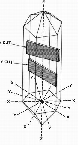
Figure 17. Major axes quartz crystal.
CRYSTAL CUTS
The natural quartz crystal, as shown in Fig.17, is said to have three major axes at right angles to each other. These axes, called the X, Y, and Z axes, are shown in the illustration. The X axis is called the electrical axis, the Y axis is called the mechanical axis, and the Z axis is called the optical axis. The way that the crystal wafers are cut with respect to these axes determines many electrical characteristics, including the frequency range in which the crystal will oscillate and the amount that the resonant frequency will change with changes in the temperature (the temperature coefficient). If the crystal wafer shown by the shaded section in Fig.17 is cut so that its face is perpendicular to a Y axis, it is called a Y-cut crystal. Similarly, if its face is perpendicular to an X axis, it is called an X-cut crystal. Crystal wafers cut perpendicular to the Z axis have no piezo electric properties.
Crystal cuts can be made at different angles to the major axes to produce crystals having slightly different electrical characteristics. The type of cut depends on the purpose for which it is to be used.
One of the most important characteristics of a quartz crystal used in oscillator circuits is the amount the crystal frequency varies with variations in temperature. We call this the temperature coefficient of the crystal. Y-cut crystals have a range of about - 25 to +100 Hz/C/MHz (Hz per degree centigrade per MHz). In other words, a one-degree centigrade increase in temperature may cause the frequency to decrease as much as 25 Hz, or increase by as much as 100 Hz for each MHz of the frequency for which the crystal is ground. To take an extreme case, the frequency of a 4-MHz crystal might increase by 400 Hz for each degree of temperature change. Because of this rather high temperature coefficient and also because Y-cut crystals have a tendency to oscillate at a second frequency near the design frequency, they are seldom used.
X-cut crystals have a range of about - 10 to - 25 Hz/C/MHz. The minus sign means that the crystal frequency decreases with an increase in tempera ture. We call this a negative temperature co efficient. Even though the frequency variation is less, close temperature control is still required to keep the crystal oscillating at the correct frequency.
As an example of how temperature affects the crystal frequency, consider an X-cut crystal that has an operating frequency of 4650 kHz at 50°C. If it has a temperature coefficient of - 20 Hz per degree centigrade per MHz, let's determine what its operating frequency would be if the temperature changes 10°.
4650 kHz = 4.65 MHz
Therefore, the change in frequency per degree centigrade is:
4.65 X 20 = 93.00 Hz
The change in frequency with a temperature change of 10° will be:
and
93 X 10 = 930 Hz
930 Hz = 0.930 kHz
Thus we see that with a temperature change of only 10°, the frequency will change almost 1 kHz.
With a 20° change, the frequency change would be almost 2 kHz. If the temperature increases 10°, the frequency will decrease to about 4649 kHz (4649.07 kHz), and if the temperature drops 10°, the frequency will increase to almost 4651 kHz (4650.93 kHz). Where there are many stations operating on frequencies close together, this shift in frequency could be enough to cause interference.
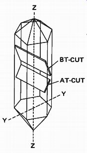
Figure 18. AT-cut and BT-cut crystals are cut on an angle to the Z
axis as shown.
We can reduce the temperature effect on the resonant frequency of the crystal by cutting the crystals at angles to the major axes. Examples of such crystal cuts, called the AT-cut and the BT-cut, are shown in Fig.18. These crystals are really Y-cut crystals with the face of the wafer at an angle of about 39° to the Z axis instead of parallel to it in the case of the AT-cut crystal, and about 45 ° to the Z axis in the case of the BT-cut crystal. Notice that the angle of the AT-cut crystal is opposite to that of the BT-cut crystal with respect to the Z axis. The temperature coefficient of these cuts is about ±2 parts per million at a temperature of 40°C to 50°C. Thus, the angle cut practically cancels the effects of temperature variation on the frequency of oscillation if it is operated within the temperature range.
Other angular cuts can be made to get other electrical characteristics and effects. Some examples are the CT and DT cuts used for lower frequency operation below 500 kHz. A CT-cut crystal is cut perpendicular to the BT-cut crystal, and the DT-cut crystal is cut perpendicular to the AT-cut crystal. Another cut is the GT-cut. This crystal is cut on an angle of about 45° to either the CT- or DT-cut crystals.
Figure 19 illustrates the variation of the resonant frequency with temperature for various crystal cuts. Notice that the frequency of the GT-cut crystal is practically constant from 0° to about 100°. This cut, therefore, is the best to use in equipment that will be subjected to wide temperature variations. The other cuts have zero temperature coefficients at or near specific temperatures.
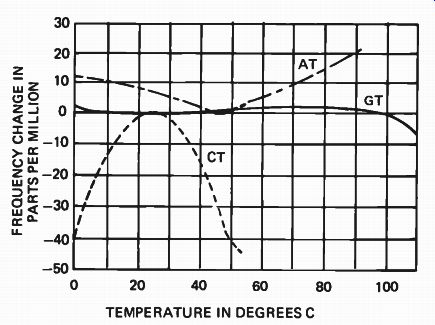
Figure 19. Frequency changes of different crystal cuts with changes
in temperature.
CRYSTAL HOLDERS
After the crystal has been ground, or etched by means of chemicals, until it is of the proper thickness, it is placed in a holder. The holder is then sealed so that no air, dirt, or oil can reach the crystal wafer. These can cause erratic operation of the crystal. A crystal in its hermetically sealed holder is shown in Fig.20.
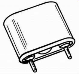
Figure 20. A quartz crystal in its holder.
There are two ways of mounting the crystal in the holder. In one way, a very thin film of metal is formed directly on the surface of the crystal by spraying or firing. The metal can be either silver, gold, or aluminum. The crystal is supported by flexible wires fastened to this metallic film with solder having a low melting point. The leads are attached to a node or non-oscillating portion of the crystal. The node can be either in the center of the crystal face or at an edge where inhibiting the vibrations will do no harm.
Another method of mounting the crystal in a holder is to arrange it so that it is pressed between two metal plates. The metal plates make electrical contact with the crystal surfaces. Another type uses an air gap 0.001 to 0.005 inch thick between the crystal and the upper plate. This air gap produces a damping effect on the amount of crystal vibration. Often, however, the crystal holder is evacuated so that the damping will be reduced.
Regardless of the type of mounting used, the holder itself is designed to keep the crystal free of grit, dirt, and oil film. Even a speck of dirt or a greasy film can change the characteristics of the crystal. Therefore, the crystal holder should never be opened, nor should the crystal be handled. If it is ever necessary to take one apart, the crystal may be cleaned with a good nonflammable commercial cleaner. The crystals should be handled with clean, lint-free cloths, not with bare fingers (bare fingers leave traces of perspiration on any object they touch).
Equivalent Circuit. The symbol in Fig.21(A) is used in schematic diagrams to represent the crystal in its holder. The equivalent electrical circuit of the crystal and holder assembly is shown in Fig.21(B). As you can see, we have here a series-parallel circuit composed of the series components L, R, and C1 shunted by capacity C2. The crystal, therefore, acts electrically as an LC circuit; as an inductance at frequencies above the resonant frequency and as a capacitance at frequencies below resonance. The apparent inductance L is due to the mass of the crystal, resistance R is the result of internal mechanical losses, and capacity C1 is the stiffness (piezoelectric properties) of the crystal.
Capacity C2 is the capacity between the electrode plates, with the quartz crystal acting as the dielectric.
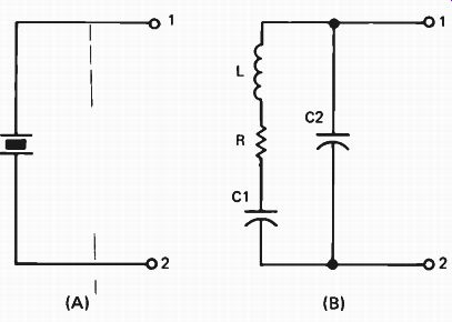
Figure 21. The schematic symbol for a quartz crystal in its holder
is shown at (A). The equivalent electrical circuit of a quartz crystal
is shown at (B).
Since the crystal acts as an electrical resonant circuit, we would expect it to be frequency selective; that is, it will oscillate more vigorously at its natural resonant frequency than at any other frequency. This is true. When an ac voltage is applied to its electrodes, the crystal generates an alternating potential of its own.
Because of its electrical characteristics, the crystal can be used in an oscillator circuit. The electrical properties of the crystal are somewhat different from those of a typical coil and capacitor.
The mechanical properties of the crystal produce a very high apparent inductance, L. Also, since the mechanical losses during vibration are small, the electrical equivalent resistance is also very small.
When we have an LC circuit containing a large inductance and a very low resistance, the Q of the circuit will be very high. This is the case with the crystal used in oscillator circuits.
Practical crystals have effective Q values which are about 100 times as great as that ordinarily obtainable with the usual inductance coil and tuning capacitor. Crystals, therefore, have extremely good frequency selectivity. The higher the Q, the better the frequency stability. Thus, if we substitute a crystal for the ordinary LC tank circuit, we can make an oscillator that has good frequency stability.
CRYSTAL OVENS
The purpose of a crystal oven is to maintain the crystal at a constant temperature to prevent frequency drift. Some time ago, it was common practice to put the crystal, the entire master oscillator of the transmitter, and often even the buffer stage in a heat-controlled chamber. This prevented temperature variations from affecting the physical dimensions of the coil and capacitor in the plate circuit, and thus changing the oscillator frequency. This is seldom done in modern transmitters; generally only the crystal is temperature controlled.
A typical modern crystal oven is shown in Fig.22. The overall unit is about the size of a metal receiving tube - about 4 inches high and 1-1/4 inches wide. Smaller units are also available. The crystal oven unit fits into an octal tube socket. The unit in Fig.22 is guaranteed to hold the transmitter frequency within 10 Hz at any point on the broadcast band.
The crystal is contained in a ceramic holder attached to a copper support. The heater is also wrapped around this support. Thus, the metal support conducts the heat to the crystal and maintains it at a constant temperature.
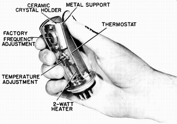
Figure 22. A cutaway view of a crystal oven.
The heat is controlled by a bimetallic thermo stat attached to the metal support. When the temperature of the support drops a very small amount, the thermostat contacts close, and current is applied to the heater. When the support reaches a certain temperature, the thermostat contacts open. The difference between the on and off temperatures of the thermostat is very small; that is, the temperature must drop only a small amount before current is again applied to the heater coil.
The crystal frequency and thermostat tempera ture adjustments shown in Fig.22 are set at the factory when the unit is assembled. It is impossible to change the adjustments because the unit is hermetically sealed. Thus, when ordering such a crystal unit, you must specify the exact crystal frequency you want and the circuit in which the crystal will be used. Crystal manufacturers will not guarantee the operating frequency of a crystal unless the crystal is adjusted in the circuit in which it will be used.
CRYSTAL OSCILLATOR CIRCUITS
To help see how the crystal oscillator works, let's look at another LC oscillator. This oscillator is shown in Fig.23, and is called a tuned-grid, tuned-plate oscillator. It is easy to see where this oscillator gets its name, since there are resonant circuits in both the grid circuit and the plate circuit of the tube.
The tuned-grid, tuned-plate oscillator works because of the capacity between the plate and grid of the triode tube. When the resonant circuit in the plate circuit of the tube is tuned to a frequency slightly lower than the operating frequency, it will act like an inductance. Under these conditions, the phase of the signal voltage fed from the plate of the tube back to the grid of the tube is correct to aid the ac grid voltage, and oscillation occurs.
The crystal oscillator shown in Fig.24 is simply a modification of the tuned-grid, tuned-plate oscillator shown in Fig.23. Here a crystal has been substituted for the resonant circuit in the grid circuit of the oscillator, and a milliammeter is shown in the plate circuit of the stage to measure plate current. Actually, almost all oscillators have some provision made for measuring plate current.
Since the crystal is the equivalent of the circuit that has been removed, the crystal oscillator operates in exactly the same way as the resonant circuit in the grid of the tuned-grid, tuned-plate oscillator. The plate circuit must be tuned so that it presents an inductive load, and energy will be fed from the plate of the tube back to the grid in the correct phase to aid the ac grid voltage so oscillation will occur.
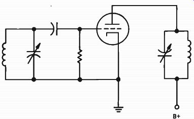
Figure 23. A tuned-grid, tuned-plate oscillator.
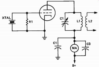
Figure 24. A simple crystal-oscillator circuit.
In the input circuit, the rf current flowing through the crystal itself is limited only by the resistance of R1. This resistance is usually low enough to result in a fairly high crystal current. If the resistance is made too high, the crystal may be somewhat erratic as it starts to oscillate when power is applied to the stage. On the other hand, if the current becomes higher than about 100 ma, the crystal vibrations may be so violent that the crystal may shatter, and thus destroy itself. Of course, the thinner the crystal and the higher its resonant frequency, the lower the safe current limit be comes.
Many transmitters have an rf current meter in series with the crystal to indicate this current. To prevent possible damage to the crystal, the amplitude of oscillation in a crystal oscillator circuit must be kept at a safe level. Usually this is accomplished by keeping the plate voltage on the oscillator tube low. This low plate voltage reduces the maximum output power that can be obtained from such oscillators.
Pierce Oscillator. It is possible to place the crystal between the plate and grid circuits, as shown in Fig.25, instead of between the grid and cathode. In this case the circuit is similar to the ultra-audion circuit. This circuit is called the Pierce oscillator.
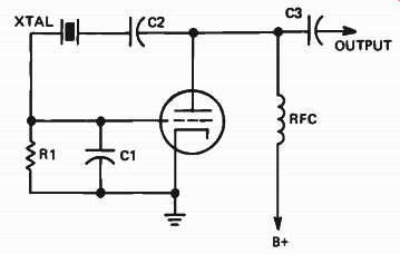
Figure 25. The basic Pierce oscillator.
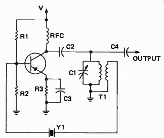
Figure 27. Crystal tickler coil oscillator.
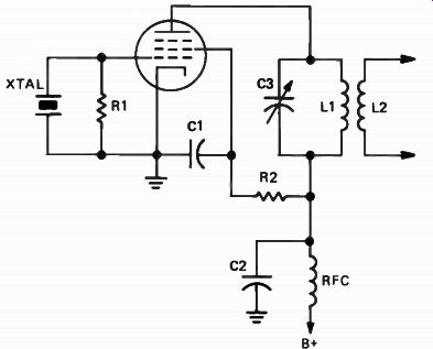
Figure 26. Crystal oscillator using a pentode tube.
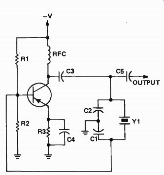
Figure 28. Colpitts crystal oscillator.
Notice that the circuit contains no tank inductance or tuning capacity. The amount of feedback and the grid excitation can be controlled to some extent by adjusting the capacity of C1. The larger this capacity, the less the feedback. The exact capacity of C1 in most cases is not critical. Usually, when the best value is determined, crystals of slightly different frequency can be switched into the circuit without further adjustment. Again the plate voltage must be low to prevent damaging the crystal.
Crystal Oscillators Using Multi-Grid Tubes
Tetrode and pentode tubes also may be used in crystal-oscillator circuits. These tubes have less plate-to-grid capacity than do triodes, and there fore, there is less feedback current to the grid when they are used as crystal oscillators. The lower feedback means that these tubes can be operated at a higher output power than a triode without excessive rf crystal current.
A crystal oscillator using a pentode tube is shown in the diagram of Fig.26. Because of the limited amount of plate-grid feedback, the plate voltage can be considerably higher than for the triode oscillator. This, of course, increases the output power. The circuit may also be used for high-frequency crystals having fundamental resonant frequencies of about 10 MHz. The output in this case can be high, but the small amount of current through the crystal protects it from excessive vibration. Sometimes extra feedback is needed to produce oscillation in the circuit. This is done by connecting a small capacitance between the plate and the control grid.
Crystal Control Transistor Oscillators. A transistor tickler coil oscillator using a crystal to control feedback is shown in Fig.27. Positive feedback from collector to base is provided through the mutual inductance between the windings of T1. This provides the 180° phase shift necessary to sustain oscillation. In this circuit, the crystal acts as a series-resonant circuit. At frequencies other than the resonant frequency the crystal acts as a high impedance, blocking the feedback path. At the resonant frequency the crystal offers minimum impedance to the feedback signal. The operating frequency may be varied by the use of different crystals and tuning the tank to the frequency of the crystal with C1.
The crystal oscillator shown in Fig.28 is a variation of the Colpitts oscillator. In this circuit the crystal acts as a parallel tuned circuit and replaces the LC tank. Operating frequency is determined by the crystal and the capacitance in series with it. At the resonant frequency, the crystal and capacitors in parallel with it form a high impedance tank circuit. Capacitors C1 and C2 form a voltage divider that is center-tapped to ground. The voltage developed across C1 is applied between the base and ground providing a 180° phase shift in the feedback path.
OVERTONE OPERATION
Most crystals will oscillate not only at their fundamental resonant frequencies, but also at odd overtones of the fundamental. A crystal with a fundamental of 4 MHz, for example, will oscillate also at frequencies near 12 MHz, 20 MHz, 28 MHz, etc. The oscillation frequency will not be an exact multiple of the fundamental oscillation frequency.
Exact multiples would mean harmonic operation rather than overtone operation. Thus, if you use a crystal designed for fundamental operation as an overtone crystal, you can use the frequency markings on the crystal holder only to get an approximate idea of the actual frequency at which the oscillator is working. To determine the exact frequency, you will have to measure it with a frequency meter.
Although any crystal can be used in overtone operation, it is best to use one that has been ground specifically for this purpose. The ordinary fundamental type of crystal is somewhat unstable and hard to adjust when operated on an overtone.
Most of the overtone crystals are designed to operate on the third overtone; operation at higher overtones is possible, but the stability and ease of adjustment becomes more critical at the higher overtones.
The chief advantage of overtone operation is that we can generate frequencies in the vhf range without the use of doubler stages. The highest fundamental oscillation frequency of a crystal is about 10 MHz. If one is ground to operate on a higher frequency, it is so thin that it breaks easily.
Thus, by operating it on the third or fifth harmonic, we get a much higher frequency than we could on the fundamental. Another advantage of overtone operation is that no frequencies are generated that can cause interference with other channels. Because the number of frequency multi plier stages is reduced or completely eliminated, overtone crystals are used often in mobile, marine, and aircraft transmitters in which compactness is important.
The oscillator circuit using an overtone crystal is similar to an ordinary crystal oscillator circuit of the type you will study later. The overtone at which the crystal will operate is determined by the plate circuit resonant frequency. The circuit of an overtone oscillator is shown in Fig.29. The oscillator uses a crystal having a fundamental frequency of about 8 MHz to give a 24 MHz output when operated on the third overtone.
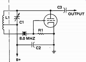
Figure 29. An overtone oscillator circuit.
In Fig.29, the circuit made up of C1 and the upper end of LI is resonant at 24 MHz. The tap on L1 is held at rf ground potential by C2. The lower end of L1 is inductively coupled to the upper end (usually this is a simple one-tapped coil) so energy is fed from the plate circuit back to the grid circuit to sustain oscillations. The rf signal fed back to the grid circuit will cause the crystal to oscillate on its third overtone frequency. Output from the oscillator is taken from the plate circuit through C3.
Modern overtone crystals are capable of oscillating as high as 100 MHz on higher order harmonics, so the output of a crystal oscillator could be up in this region. However, when such high-frequency signals are needed, you will often find a crystal oscillator operating at 50 MHz followed by a doubler to increase the frequency to 100 MHz, or an oscillator operating at about 33.3 MHz followed by a tripler.
An oscillator circuit that can be used to generate both even and odd harmonic frequencies of the fundamental is the tri-tet circuit shown in Fig.30. The output signals are harmonics rather than overtones.
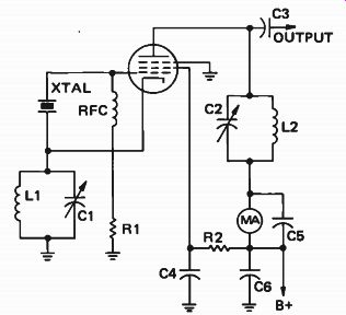
Figure 30. The tri-tet oscillator circuit.
The tri-tet circuit is actually the crystal version of the electron-coupled circuit described earlier in this lesson. The crystal and the resonant tank L1- C1 are connected to the control grid, the cathode, and through C4 to the screen grid (which acts as the oscillator plate), to form a modified tuned-plate, tuned-grid oscillator. The cathode tank circuit L1-C1, therefore, must be tuned to a frequency slightly lower than that of the crystal in order to be inductive.
Since the screen grid is bypassed to ground by capacitor C4, there is very little direct coupling between the actual tube plate and the oscillator portion of the circuit. The electron stream reaching the plate, however, arrives in the form of pulses that contain relatively large amounts of harmonic energy. If we tune the plate tank circuit L2-C2 to a frequency twice that of the crystal, a considerable amount of output power at the second harmonic frequency will be obtained. Even if the plate is tuned to a frequency three times that of the crystal we will get a fair amount of third harmonic output power.
Therefore, the tri-tet circuit not only behaves as a crystal-controlled oscillator, but also performs as a frequency doubler or tripler at the same time.
The additional feature of the electron coupling prevents load variations from reaching the crystal and influencing the oscillator frequency. A disadvantage of this circuit is that both sides of the crystal are above rf ground potential. Another is the fact that a cathode coil is needed.
CRYSTAL-OSCILLATOR ADJUSTMENT
The tuning procedures for crystal oscillator circuits of all types are similar. The curves in Fig.31 show how the plate current of an oscillator tube varies with changes in the tuning capacity.
The solid curve is for an unloaded oscillator circuit, and the dashed curve represents the circuit loaded.
When you adjust a triode or Pierce oscillator like those shown in Figs.24 and 26, begin first with the plate tank capacitor in the minimum capacity position. Then rotate the capacitor toward the maximum capacity position. As soon as oscillation begins, the plate current will begin to decrease. It will decrease more and more, going through points 3 and 2 in Fig.31 as oscillation becomes stronger.
If the plate capacitor is turned too far, however, oscillations will stop abruptly as at point 1 in Fig.31. In practice, it is best not to approach point 1 too closely because minor voltage or current variations may stop the oscillator. Instead, adjust the plate tuning capacitor so that operation will be somewhere in the stable region between points 2 and 3.
When a load is placed on the oscillator circuit, the plate current dip of the oscillator will not be as pronounced. It will follow the dashed curve in the diagram. As before, however, too much capacity will cause the oscillator to stop. The operating point again should be somewhere between points 2 and 3.
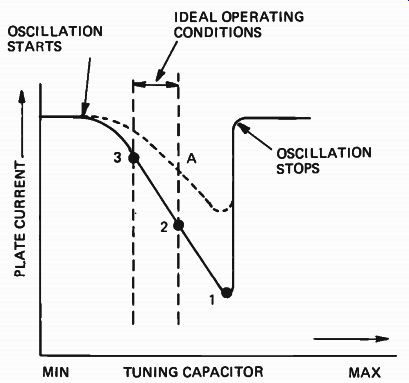
Figure 31. Curves showing how the plate current in a crystal-oscillator
circuit varies with tuning.
The transistor oscillator in Fig.27 would be adjusted in a similar manner, C1 being tuned to a point where the current through the tank is between points 2 and 3 in Fig.31. C1 is first tuned for minimum capacitance. Then the capacitance is increased until current is between the stable points of operation.
When adjusting the tri-tet circuit in Fig.30, first set the cathode tank capacitor C1 to a frequency higher than resonance (minimum capacity) so that oscillations will occur. In this circuit, the usual parts values are such that oscillation will be maintained over a fairly wide range of the C1 adjustment. However, the crystal current increases very rapidly as the capacity is increased. Start tuning C1 for the minimum capacity position and progress only to the point of normal crystal current.
Usually an rf milliammeter is placed in series with the crystal to measure this current. The current should be kept below 100 ma.
With no load connected, the plate tank capacitor C2 should be adjusted for a minimum value of plate current as indicated by a sharp dip in the meter reading. Now, connect the load to the circuit. This is usually the grid of the following buffer amplifier stage. With the load attached, capacitor C2 may need readjustment to bring the plate current back to minimum. This time, how ever, the current value will be somewhat higher because of the loading.
Finally adjust the cathode tank capacitor C1 for maximum harmonic power output which will be indicated by a maximum current flow in the following amplifier grid current. Also watch the crystal current to be sure that it does not rise above the safe limit.
SELF-TEST QUESTIONS
15. Why is plate voltage kept low in the Pierce oscillator?
16. Describe how frequency is controlled in the oscillator in Fig.27.
17. What is the advantage of overtone operation?
18. In the multiple crystal frequency synthesizer in Fig.32, what is the output of the mixer if S1 is in the 80 kHz position and S2 is in the 1300 kHz position?
19. In addition to performing as an oscillator, what other function is accomplished by the tri-tet oscillator?
++++++++++++++++++++++++
Frequency Synthesizers
Several communications services require equipment capable of operation on many different frequencies. Two good examples are the class D citizens band and the aircraft navigation and communication band. If this equipment used the crystal oscillators discussed previously, the crystal would have to be changed each time operation on a different frequency was required. In most cases, the equipment is a transceiver which allows both transmitting and receiving on a channel. This equipment would require two crystals for each channel, one to control the frequency of the transmitter and another to control the frequency of the receiver local oscillator. This method is satisfactory as long as operation on only a few channels within a band is desired. However, in the case of a class D CB transceiver, forty-six crystals would be needed for operation on all the channels! The cost of the crystals alone would make the unit quite expensive. A frequency synthesizer provides a good solution to this problem.
A frequency synthesizer is a circuit which produces a sizable number of frequencies, each having the stability and accuracy that would normally be obtained only by using individual crystal oscillators. There are two major types of frequency synthesizers in use today. They are the multiple crystal type and the digital phase-locked loop frequency synthesizers. The multiple crystal synthesizer currently enjoys the widest use; but, the digital frequency synthesizer is rapidly gaining in popularity due to the greater number of frequencies available from still fewer crystals.
MULTIPLE CRYSTAL SYNTHESIZER
Figure 32 shows a multiple crystal frequency synthesizer used in the Johnson Messenger 123A class D CB transceiver. Circuit details have been omitted for simplicity. This type of synthesizer operates on the same principle that you studied earlier in the basic superheterodyne receiver in which an incoming signal beats with the local oscillator to form two new frequencies. These new frequencies are the sum and the difference of the incoming signal frequency and the local oscillator frequency, the difference frequency being the intermediate frequency.
Figure 32. A multiple crystal frequency synthesizer used in the Johnson
Messenger 123A.
In Fig.32 you see that two oscillator circuits are used with a mixer which will beat the outputs of the oscillators together. A double-tuned circuit is used at the output of the synthesizer mixer to select the difference frequency and reject the sum of the two frequencies. Each of the oscillators is tunable to different frequencies by rotating the channel selector switch, S2A and S2B. The switch has 24 positions; however, only 23 of the positions connect the crystals to their respective oscillators to allow the transceiver to operate on one of the 23 class D CB channels. S2A connects one of the six 32 MHz crystals to the high oscillator. S2B connects either a 5 MHz crystal or a 6 MHz crystal to the low oscillator, depending on whether the transceiver is in the transmit or receive mode.
With S2 in the position shown, a 5.735 MHz crystal is selected for transmit. This signal mixes with the 32.7 MHz signal from the high oscillator to produce an output frequency of 32.7 - 5.735 = 26.965 MHz. This is CB channel 1. In the receive mode, S2B selects the 6.190 MHz crystal while the 32.7 MHz crystal still controls the high oscillator. This time the output of the mixer is 32.7 - 6.190 = 26.510 MHz and is fed to the receiver mixer as the local oscillator frequency. Since the transceiver uses an i-f of 455 kHz, a signal on channel 1 could be received: 26.510 + 0.455 = 26.965 MHz If you wish to see how the transmit and receive local oscillator frequencies for any of the other channels are generated, you could do so by mentally rotating the selector switch to see which crystals are selected. For example, imagine the switch rotors are moved one position clockwise.
S2A still selects the 32.7 MHz crystal. S2B selects the 5.725 MHz and the 6.180 MHz crystals to produce the correct transmitter frequency of 26.975 MHz and the correct receive local oscillator frequency of 26.520 MHz for operation on channel 2.
This synthesizer produces all the necessary 46 specific frequencies to allow the transceiver to cover the full 23 channels which make up the class D citizens band. Instead of requiring 46 separate crystals, only 14 are needed.
DIGITAL FREQUENCY SYNTHESIZERS
Multi-channel communications equipment being designed today seldom includes a synthesizer of the multiple crystal type. While considerably fewer crystals are needed, this system still requires far more crystals than digital phase-locked loop (PLL) frequency synthesizers. A PLL synthesizer can be designed using only one crystal in the system, yet offering an almost unlimited number of output frequencies.
These systems were not designed into earlier equipment due to the lack of integrated circuit "building blocks" containing the various circuit functions necessary for constructing a PLL system.
Without them, the cost of constructing even a simple system using individual transistors and other components would have been too high. This is especially true in the case of a unit requiring only 46 specific frequencies, such as in the unit we previously discussed.
The basic components involved in a digital phase-locked loop frequency synthesizer, in its simplest form, are shown in Fig.33. There are four major circuits in a PLL system. They are the VCO, the programmable dividers, the frequency/phase detector, and the loop filter. Notice how the circuits are connected to each other. The signal path forms a loop from the output of the VCO, through the programmable divider to the phase detector, through the phase detector to the loop filter, and through the filter back to the VCO. Thus, you can see how the system got the "loop" part of its name.
You may have already noticed that the phase detector has a second input which we have labeled reference frequency. It was not included in our discussion of the loop components because it is not "in the loop." In other words, it is not affected or changed in any way by changes in any of the loop components. The loop components affect each other directly. A change in any one of them will cause a change in the other three.
Let's examine each of the loop components a little more closely. The block in Fig.33 labeled VCO is the frequency generating component of the PLL system. VCO stands for voltage-controlled oscillator. The frequency of the oscillator's output changes in proportion to the applied control voltage. Let's see how such a circuit might be implemented.
Figure 33. The basic digital phase-locked loop frequency synthesizer.
Figure 34. A Hartley voltage controlled oscillator.
A Voltage Controlled Oscillator. A dual-gate MOSFET is used as the active device in the Hartley oscillator circuit shown in Fig. 34. Since you have already learned about the operation of a Hartley oscillator, we will not cover it again here. The important component to notice in Fig.34 is the diode D1.
You will recall from a previous lesson that the capacitance of a diode junction will decrease if the reverse bias voltage across the junction increases.
D1 is a special junction diode called a varactor diode whose capacitance versus voltage characteristic is linear and predictable. Since the diode is connected in series with C2, across the tank circuit, the frequency of the oscillator will increase as the applied voltage increases. The lower frequency limit of the tank circuit is adjusted by C3 with zero volts, or the minimum expected voltage, applied to Dl through R1 . Multivibrators. The oscillators you have studied up to this point have all been sine wave oscillators; that is, their output is a sine wave. The output of the oscillator we are about to discuss is not a sine wave and therefore is referred to as a nonsinusoidal oscillator. An oscillator of this type is generally classified as a relaxation oscillator. A relaxation oscillator uses a regenerative circuit in conjunction with an RC circuit to provide a switching action.
The RC time constants control the shape and frequency of the output waveforms.
Let's examine the circuit in Fig.35. This is an astable or free running multivibrator. A multi vibrator is a two-stage oscillator in which one stage conducts while the other is cut off, until a point is reached at which the stages reverse their conditions. The output of each stage is coupled to the input of the opposite stage. The output signal of the stage is a square wave whose frequency is determined by the RC time constants in the feedback loops.
In the circuit in Fig.35, one of the transistors will conduct a little harder than the other when power is applied due to the slight differences that exist between any two transistors, even of the same type. Let's assume that Q1 conducts hardest. The collector current flowing through R1 will cause the voltage at the junction of R1 and C1 to go in a negative direction. This negative pulse is fed through C1 to the base of Q2, cutting off its conduction. This causes the voltage at the junction of R4 and C2 to increase. The positive-going pulse is coupled through C2 to the base of Q1, causing it to go into saturation.
Once QI is saturated, there is no change in the voltage level at the junction of R1 and C1; therefore, the base of Q2 begins to go positive as C1 charges up through R3. Soon, Q2 begins conducting, producing a negative-going pulse at its collector. This pulse is fed through C2 to the base of Q1 and starts reducing the transistor's conduction. The resulting positive-going pulse at the collector of Q1 is coupled through C1 to the base of Q2, driving it into saturation. Q1 is driven to cutoff.
Figure 35. An astable multivibrator.
Figure 36. A voltage-controlled multivibrator (VCM).
This process continues until the power is removed from the circuit. The rate at which the circuit changes state is controlled by the time constant of R3-C1, R2-C2, and the B supply voltage. If the two time constants are exactly equal, the output signal will be a symmetrical square wave.
There are variations of the astable multi vibrator called the monostable and the bistable.
Trigger pulses are required for these two circuits.
When the monostable is triggered, it will change state, remain in the new state for a short time, then return to the state it had before the arrival of the trigger pulse. The bistable has two stable states. It will change state upon the reception of a trigger pulse and remain in the new state until a second pulse is received. This circuit is used in digital flip-flops such as those you studied in an earlier lesson.
Voltage-Controlled Multivibrator. The circuit in Fig.36 is one which can readily be used as a low frequency VCO. The circuit could more accurately be referred to as a voltage-controlled multivibrator, VCM. The only difference between this circuit and the one we just discussed is the addition of the two junction field-effect transistors Q2 and Q3. They allow the frequency of the multivibrator to be controlled by an external voltage. R2 and R3 are current limiting resistors, used to ensure that the FET's are not destroyed by excessive current. The applied control voltage changes the channel resistance of the FET's and causes them to perform as though they were variable resistors. Since they are the timing resistors for the RC circuits, the frequency of the multivibrator changes. Thus we could use this circuit if we wished to construct a low-frequency VCO for a phase-locked loop frequency synthesizer.
Programmable Dividers. Let's examine the next component in the PLL, the programmable divider.
This circuit allows the output frequency of the synthesizer to be changed according to the number on the divider's programmable inputs.
We have shown a diagram of a type D (data) flip-flop in Fig.37 together with its associated truth table. The table tells how the flip-flop will per form, depending upon the condition of its inputs.
It will divide an incoming signal by two, the same as other flip-flops you studied in an earlier lesson.
The thing which makes the type D flip-flop particularly useful in a programmable divider is its preset and clear inputs. These allow the state of the outputs to be changed, or set up, prior to the dividing operation. Let's go over the operation of the type D flip-flop.
Remember, the 0 condition means a low voltage level and the 1 condition means a high voltage level. Further, you will see both X and an arrow pointing up in the INPUTS column of the truth table shown in Fig.37. The X means the input "doesn't care" whether it is high or low. The outputs will be as shown regardless of the condition of this input. The upward pointing arrow at the bottom of the CLOCK column means that the outputs change to the state shown on the positive going or leading edge of the clock pulse.
The preset and clear inputs of the type D flip-flop are "active low." In other words the flip-flop is set when the preset input is pulled low, toward ground. The clear input must remain high.
The state of the clock and D inputs may be either high or low. The Q output will be set to a logic 1 and the to a logic 0. When the preset input remains high and the clear line is pulled low, the outputs will be set to the opposite state; Q will be low and rj will be high. It is only necessary to pull the preset or clear inputs low momentarily to set or clear the flip-flop. The outputs will remain set or cleared when the selected input .returns to its inactive or high state.
An illegal set operation is possible when both inputs are pulled low at the same time. This operation is not normally used since both the Q and outputs will be set high but they will not remain in this state when the inputs return high.
Further, it is not known exactly what state the outputs will assume once the preset and clear inputs return to their inactive condition.
When the preset and clear inputs remain inactive, the logic level appearing at the D or "data" input of the flip-flop will be transferred to the Q output on the positive-going edge of the clock signal.
Four type D flip-flops can be connected together using additional logic to form a programmable decade counter which can be made to divide by any whole number from 1 to 10. Such a divider is called a programmable decade counter and is available as a single integrated circuit. The incoming signal is applied to the clock input of the first flip-flop. The D inputs are connected to cause the flip-flops to divide by 10 through the use of feedback connections. If four stages were merely connected with the Q output of one feeding the clock input of the following flip-flop, the divider would divide by 16 instead of 10. This is the difference between a straight binary counter and a decade or binary coded decimal (BCD) counter.
Four-bit (four stage) binary counters are some times used as programmable dividers, but most PLL systems use decade counters for easier programming.
Figure 37. A type D flip- flop and its truth-table.
Figure 38. A typical loop filter.
The programmability comes about through additional logic which allows the counter to be preset to any number between 0 and 9. This will cause the counter to count down from the preset number, effectively dividing the incoming number by the preset. The programmable inputs are also masked to allow the counter to divide by 10 or by the preset number.
Phase Detectors and Loop Filters. The next component in the phase-locked loop is the phase detector. You will recall from Fig.33 that the phase detector has two inputs and one output. One input receives a signal from the programmable divider. This signal is compared with the frequency and phase of a signal entering the second input of the phase detector called the reference frequency.
If there is a frequency or phase difference between the two signals, a series of pulses appears at the output of the phase detector. The pulses occur at the rate of the reference frequency, but vary in width, or duration. These pulses are fed to the next component in the PLL system, the loop filter.
A schematic diagram of a simple loop filter is shown in Fig.38. The purpose of the filter is to smooth out the pulses from the phase detector until they become essentially a pure dc voltage.
This control voltage is then fed to the VCO to control its frequency.
Now that you have seen each of the major components involved in a basic digital phase-locked loop frequency synthesizer, let us see how they work together.
The VCO is responsible for generating the output signal. The programmable divider divides the VCO frequency so that it is within the range of the control system. If the number (N) programmed into the dividers is changed, the phase detector generates a voltage of the proper polarity and amplitude to steer the VCO frequency in the direction that will bring the frequency coming from the dividers back to the reference frequency.
Programming is usually accomplished with BCD thumbwheel or rotary switches.
• The reference frequency is usually derived from a stable, crystal-controlled oscillator whose frequency is divided down to the desired reference frequency. For example, the reference frequency used in a synthesizer designed for the aircraft band would be 25 kHz, since that is the channel spacing on that band. The channel frequency is displayed, at the control panel of the unit, on the programming switches. The unit would be capable of covering 118-136 MHz in 25 kHz steps for a total of 720 channels. Imagine how many crystals that would require - even for a multiple crystal frequency synthesizer!
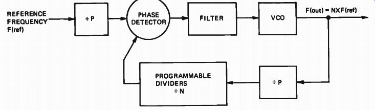
Figure 39. A PLL synthesizer using pre-scaling.
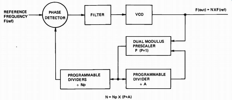
Figure 40. A dual modulus prescaler synthesizer.
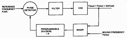
Figure 41. A synthesizer using down mixing.
Direct Frequency Synthesizer. There are two major types of digital PLL frequency synthesizers.
They are generally classified as direct or indirect.
The classification refers to the manner in which the output of the synthesizer VCO is used. If the VCO output is fed to a multiplier or mixer before it is actually used, the synthesizer is considered to be indirect. If the output of the VCO is used directly, it is of the direct type. The synthesizer we have been discussing is one of these. The output frequency is equal to the number programmed (N) times the reference frequency [ F (ref)]. There are several ways to implement both direct and indirect synthesizers. They may be classified more specifically. We will briefly discuss three more direct synthesizers.
The frequency synthesizer shown in Fig.39 uses a fixed divisor (+ P) prescaler between the VCO and the programmable dividers. This technique is used to increase the upper frequency limit of the synthesizer. The programmable dividers are not capable of working up into the vhf range. Fixed dividers are readily available up to 1 GHz (1000 MHz). Unfortunately, the reference frequency must also be divided the same amount to maintain the same frequency steps of the basic direct synthesizer discussed earlier. Since a lower frequency is used as the reference, it is more difficult to filter and slows down the response of the loop to frequency changes.
Another type of direct synthesizer is shown in Fig.40. It is called a dual modulus prescaler PLL. Modulus is just another way of saying divisor. In other words, the prescaler used in this synthesizer is capable of dividing by two different divisors. The divisor is selected by another programmable divider called the A counter.
Divisors of 10 and 11 are frequently used in a dual modulus prescaler. The number programmed into the A counter tells the prescaler how many times it has to divide by 11. This technique allows the synthesizer output to be changed in steps equal to the reference frequency. Its advantage over the prescaler synthesizer previously discussed is that the reference frequency is not divided down to a lower frequency. The loop response is fast and performs just like the basic PLL synthesizer discussed first.
There is an alternate method of getting the output of a vhf synthesizer down to a frequency the programmable dividers can handle. This involves using a mixer to heterodyne the output of the VCO down to a lower frequency, as shown in Fig.41. The difference frequency is selected by tuned circuits at the output of the mixer.
This method has two disadvantages, both caused by the presence of tuned circuits in the system. If a synthesizer such as this were used commercially, the manufacturer's costs would be increased by the necessity of having to align the tuned circuits. Also, the tuned circuits limit the range over which satisfactory mixing can take place. This method would be unsuitable for a synthesizer covering more than a few megahertz.
Notice that the mixer is in the loop. Therefore, any tendency toward frequency drift or instability in the mixer oscillator would be compensated for by loop action. Nevertheless, the mixer oscillator is usually crystal controlled. This is a third disadvantage over the previous synthesizers, which required only one crystal.
Indirect Synthesizers. Finally, let's take a look at a couple of indirect frequency synthesizers.
They represent two more ways in which the requirements of a vhf output from a synthesizer can be achieved while still keeping the signal fed to the programmable dividers within their range of operation.
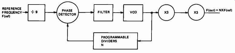
Figure 42. A multiplier PLL synthesizer.
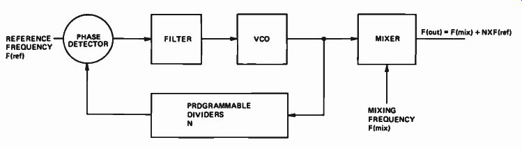
Figure 43. A synthesizer using UP mixing.
The block diagram of a multiplier PLL synthesizer is shown in Fig.42. In this circuit, the relatively low frequency output of the VCO is multiplied nine times, up to the desired frequency.
The output of the VCO is fed directly to the programmable dividers as it is well within their range of operation. The reference frequency must be divided the same number of times the VCO output is multiplied, if steps in the amount of the reference frequency are to be maintained.
In this respect, this system is like the fixed prescaler PLL. Again, the lower effective reference frequency will slow down the response time of the loop. This system has a couple of additional disadvantages caused by the multipliers. The multi pliers include tuned circuits which must be aligned.
Further, the Q of the tuned circuits must be high enough for good multiplying action, yet low enough to achieve a reasonable bandwidth.
Another disadvantage of the multiplier type synthesizer is that any subaudible disturbances of the VCO frequency may be multiplied up to the audible range. This means that a cleaner VCO and improved loop filter would be required.
Another type of indirect synthesizer is shown in Fig.43. This synthesizer uses a mixer at its output to beat the VCO frequency up to the band of interest. The unfortunate disadvantage of this technique is that the mixer is not in the loop.
Therefore, a highly stable heterodyne oscillator must be used in addition to the stable reference frequency oscillator. Even then, the stability and accuracy of the output signal will depend upon the worst case conditions of both oscillators.
There are probably many more ways in which a digital phase-locked loop frequency synthesizer could be implemented. We have shown several proven methods for accomplishing this task and discussed the advantages and disadvantages of each.
While we have not been able to give you an in-depth technical discussion, because it would be beyond the scope of this lesson, we have presented sufficient information to allow you to feel comfortable in working with communications equipment containing a digital PLL synthesizer.
SELF-TEST QUESTIONS
20. What effect would doubling the value of C1 and C2 in Fig.36 have on the output frequency?
21. What is D1 in Fig.34 called?
ANSWERS TO SELF-TEST QUESTIONS
1. Regenerative or positive feedback. If positive feedback is not present, oscillations will be damped.
2. Decrease. Frequency is equal to: 1 / 2 pi Radic LC
Therefore, if inductance increases, the frequency will decrease.
3. There will be more cycles in the wave train.
Losses in the coil of a high Q circuit are low so more cycles occur before the wave train is damped.
4. 0.0000005 second or 0.5 microsecond.
The formula is:
P = 1/f=1/2,000,000 = 0.0000005 second
5. They are in-phase. The voltage developed across L2 is the feedback voltage and must aid plate current.
6. The bias voltage developed across R1 . If the oscillator output increased, C2 would be charged to a higher potential on positive peaks and would produce a larger bias voltage across R1 . The larger bias would reduce the amplitude of the oscillator output.
7.
1. Oscillator remains energized at all times.
2. Oscillator coil and capacitor are placed in an oven.
3. Temperature compensating capacitors are placed across the tank.
8. A swamping capacitor is placed across collector-to-emitter junction.
9. R1 and C2 develop the negative bias. L2 develops the signal.
10. It goes positive. The reactance of C2 is small at the resonant frequency of the tank; there fore, the positive voltage induced in the tank by L2 (voltage across C1) is coupled to the grid.
11. C1 develops the feedback voltage. It is applied to the base through C3 and across R1.
12. The ultra-audion oscillator is a modification of the Colpitts circuit.
13. Through the RC phase shift network in the grid. Each pair of RC components shifts the phase a definite number of degrees. Total shift through all stages must equal 180°.
14. R2 and C2 develop the feedback voltage.
15. To prevent damage to the crystal.
16. Frequency is controlled by the crystal, Y1. At the resonant frequency, Y1 offers minimum impedance to the feedback voltage. At other frequencies, impedance increases.
17. A higher frequency can be obtained without the use of frequency multipliers.
18. 1380 kHz.
19. The tri-tet oscillator functions as an oscillator and a frequency multiplier.
20. The output frequency would be halved.
21. A varactor diode.
Lesson Questions
Be sure to mark your lesson card as shown to indicate Lesson CC205. Most students want to know their grades as soon as possible, so they mail their lesson card in immediately. Others, knowing they will finish another lesson within a few days, send in two cards at once. Either practice is acceptable. However, don't hold your answers too long; you may lose them. Don't hold answers to more than two sets of lessons at one time, or you will run out of lessons before new ones can reach you.
1. The time it takes a resonant through one complete cycle is:
a. Its period.
b. Its frequency.
c. Its Q.
d. 0.001 µs. circuit to go
6. The temperature coefficient of an X-cut crystal is - 20 Hz/ C/MHz. What will its
2. The tube or transistor used in an rf oscillator acts effectively as:
An electronic switch.
A damper.
A constant voltage source.
A modulator.
3. If the operating voltage of an oscillator tube is changed so that the plate resistance of the tube increases, what will happen to the operating frequency?
a. Remains the same.
b. Cannot tell.
c. Increases.
d. Decreases.
4. The quartz crystal cut which shows the greatest stability with temperature variations is:
a. AT.
b. BT.
c. CT.
d. GT.
5. When adjusting the capacitance of the tank circuit in a crystal oscillator, what happens to the plate current as oscillations start?
It rises rapidly.
It starts to decrease.
Nothing.
It drops sharply.
oscillating frequency be at 65°C if its frequency is 5250 kHz at 50°C?
a. 5251.575 kHz.
b. 5248.323 kHz.
c. 5248.425 kHz.
d. 5250.157 kHz.
7. In Fig.11(B), the ratio of what two parts determines the amount of feedback applied to the base?
a. R1 to R3.
b. C3 to LI.
c. C1 to C2.
d. C3 to R1.
8. For what part of the cycle does plate or collector current flow in an LC oscillator circuit?
Less than one-half cycle.
One-half cycle.
Three-quarters of a cycle.
One full cycle.
9. An LC oscillator whose frequency can be: varied by changing a control voltage is a:
a. VCM.
b. Hartley oscillator.
c. VCO.
d. Colpitts oscillator.
10. The four major circuits in a basic phase-locked loop (PLL) are the programmable divider, loop filter, and:
a. Frequency modulator, VCO.
b. Phase detector, VCO.
c. Lock detector, VCO.
d. Phase detector, multiplier.
Based on: NRI Schools (courses)-- A Division of The McGraw Hill Companies Washington, DC 20008, USA.
| Top of Page | Index | PREV | NEXT |