AMAZON multi-meters discounts AMAZON oscilloscope discounts
Contents:
INTRODUCTION
THE AMPLITUDE-MODULATED SIGNAL
Modulation Percentage
How Sidebands are Formed
Sideband Power
Antenna Current
Modulation Distortion
Amplitude-Modulation Systems
PLATE MODULATION
A Plate-Modulated Triode
Plate-Modulated Push-Pull Stage
Tetrode or Pentode Plate Modulation
Heising Modulator
Adjusting a Plate-Modulated Amplifier
Collector Modulation
G RID MODULATION SYSTEMS
Control-Grid Modulation
Screen and Suppressor-Grid Systems
Suppressed-Carrier Systems
Keying a Transmitter
AMPLITUDE DEMODULATION
Diode Detectors
CW Detection
LESSON QUESTIONS
------------
Introduction
The rf signal that is amplified by the class C power amplifier stages in a transmitter can be fed to an antenna and transmitted through space to the receiving location. This signal by itself, however, is of little value. It has a single, constant frequency and a constant amplitude. Since the signal does not change in any way it cannot transmit intelligence from one point to another; but by adding an intelligence signal that changes the rf signal in some way the signal can be used to carry intelligence such as code, sound, or TV. Any process that changes or varies the rf signal so that it carries intelligence is called modulation. The intelligence signal is called the modulating signal, and the rf signal is called the carrier.
At the receiver, the modulated rf signal is amplified, and then the intelligence signal is re moved from the carrier. This process is called demodulation.
There are several ways of adding intelligence to or "modulating" a radio frequency carrier. Perhaps the simplest form of modulation is code modulation, shown in Fig. 1. With code modulation, messages are sent by switching the carrier on and off at prescribed rates and durations. The most common method of code transmission uses the International Morse Code, in which dots and dashes represent letters and numerals.
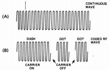
Figure 1. A code-modulated wave.
In more complex forms of modulation, sound or picture information is used to vary the amplitude, the frequency, or the phase of the carrier signal. These three forms of modulation are com pared in Fig.2. The rf carrier signal is shown in Fig.2(A) and the intelligence to be modulated on it is shown in Fig.2(B). We have used a sine wave merely for convenience; the intelligence signal actually transmitted by a radio or TV station has a very complex waveform.
In amplitude modulation (abbreviated AM) the modulating signal causes the carrier amplitude to vary in accordance with the strength of the audio signal as shown in Fig.2(C). Notice that a steady carrier is transmitted when the modulating signal is zero. When the modulating signal is applied, it causes the amplitude of the carrier to vary in step with the strength or amplitude of the modulating signal. In other words, the radio frequency output exactly follows the variations of the modulating signal.
The frequency of the carrier can also be made to vary in accordance with the strength of the modulating signal to produce frequency modulation (abbreviated FM) as shown in Fig.2(D). The amount of carrier frequency variation increases as the amplitude of the modulating signal increases, and decreases as the amplitude of the modulating signal decreases. For phase modulation (abbreviated PM), shown in Fig.2(E), the modulating signal causes the phase of the carrier, or the time interval between peaks of the carrier cycles, to vary according to the amplitude sine wave signal. The unmodulated rf carrier leads the modulated carrier at the peak of the sine wave signal, but lags the modulated carrier during the troughs. In both frequency modulation and phase modulation, the amplitude of the carrier remains constant; the intelligence to be conveyed causes only the frequency or phase of the carrier to vary.
Frequency modulation and phase modulation will be taken up later in the course. In this lesson, you will learn how the intelligence signal amplitude modulates the carrier, and study the circuits in which amplitude modulation takes place. After you have studied AM systems, you will learn how the modulated signal is demodulated at the receiver.
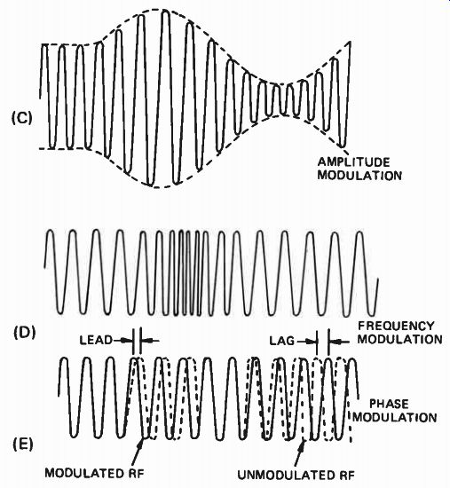
Figure 2. An rf signal can be modulated by varying its amplitude,
frequency, or phase.
--------
The Amplitude-Modulated Signal
You have learned that an amplitude-modulated signal is made up of two parts: one is a constant amplitude, constant-frequency rf signal called the "carrier," and the other is the intelligence signal - either audio or TV picture information. When the two signals are combined the strength of the carrier is made to vary according to the amplitude of the modulating signal.
Before we study the modulated wave itself, let us find out how the two signals are combined.
In a radio transmitter, the modulating or combining of the two signals is done in a power amplifier stage similar to those you have already studied. You will remember that signal amplification in a class C stage is nonlinear. Only a part of the positive alternation of the input signal causes plate current to flow. Thus, a change in the signal on the grid does not cause a corresponding change in the plate current. When you feed the audio and rf carrier signals into a class C stage, the two will beat together or "heterodyne." The two signal components add and subtract from each other to produce the waveform shape shown in Fig.2(C) and the output.
The overall outline, shown by the dashed line in Fig.2(C), is called the "envelope." Notice that each half of the modulation envelope has the same shape as the modulating audio signal. When the amplitude of the modulating audio signal increases, the amplitude of the carrier signal increases.
Likewise, when the amplitude of the audio decreases, the amplitude of the carrier decreases. The shape of the audio modulating signal, however, is not changed; it is actually superimposed on the carrier and causes the amplitude of the carrier to vary.
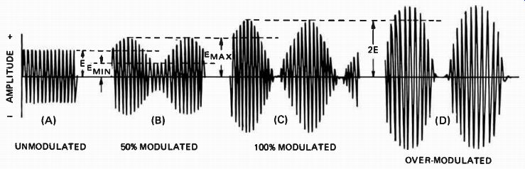
Figure 3. An unmodulated (B), (C), and (D).
OVER-MODULATED carrier is shown at (A), and the same carrier with different degrees of modulation is shown at MODULATION PERCENTAGE
The strength of the audio modulating signal applied to the class C stage determines the amount that the carrier signal will vary. Figure 3 shows an unmodulated carrier signal and several examples of various degrees of modulation. In Fig.3(B), the audio signal increases the carrier 50% above its unmodulated value (E) during the positive modulating alternation, and decreases the carrier 50% below its unmodulated value on the negative modulating alternation. The maximum and mini mum values are labeled Em Ax and Em IN in the illustration.
Now suppose the audio signal is strong enough to modulate the carrier completely; that is, it is able to drive the carrier to zero on the negative modulation alternation. The carrier is then said to be modulated 100%, as shown in Fig.3(C). At the peak of the modulating signal cycle the carrier amplitude is twice its unmodulated value, as shown in Fig.2(E). This condition represents the maximum amount the carrier can be modulated without seriously distorting the desired audio information and generating strong harmonics of the carrier signal.
The result of over-modulating the carrier by applying an excess amount of audio signal is shown in Fig.3(D). Here the audio has driven the carrier to zero for a large part of the negative modulating alternation. Thus, the envelope shape is no longer exactly the same as the audio modulating signal.
The largest amount that the carrier can be modulated without introducing distortion, therefore, is 100%. The modulation percentage is important be cause it determines the amount of power contained in the modulated signal, and thus the amount of audio signal present at the output of the audio detector in a receiver. The higher the percentage, up to 100%, the higher the output. Let us see how we can compute the percentage of modulation on the carrier.
If we know the value of the unmodulated carrier [E in Fig.3(A)] and the maximum value, Em A x , at the modulation peak, we can use the following formula: percentage modulation equals EM AX - E x 100 E For example, suppose the value of Em A X is 400 volts and the value of E is 200 volts: percentage modulation equals 400 - 200 X 100 = 100% 200 A factor that is often used to indicate how much the carrier is modulated is the degree of modulation (m). This is expressed as a decimal instead of a percentage.
(Degree of Modulation) m EM A X E E
Notice that the formula is similar to the one given for percentage modulation. Thus for 100% modulation, the value of m is 1; for 50% modulation, the value of m is 0.5, etc.
This method of computing modulation percentage is true only if the modulating signal is a sine wave. Complex sound and picture (TV) waveforms will not have the same modulation percentage over a complete cycle. The modulation of speech, music, or image signals will reach 100% only on the high-amplitude peaks. However, even the most complex sound is made up of sine wave signals. Since it is easier to visualize the modulation process with sine wave signals, we will continue to use them in our discussion.
HOW SIDEBANDS ARE FORMED
At the beginning of this section we said that the carrier and the audio-modulating signals beat together or heterodyne in a class C amplifier stage to produce the modulated waveform. Whenever two signals beat together in a nonlinear device, such as a class C amplifier, two new signal frequencies are produced. One of these signal frequencies is equal to the sum of the two frequencies beating together and the other is equal to the difference of the two frequencies beating together. Thus the heterodyning process that occurs in a class C amplifier will produce signal components that are the sum of the audio and carrier frequencies and the difference between the audio and carrier frequencies. The sum and difference frequencies are located above and below the carrier frequency and are called the "sidebands."
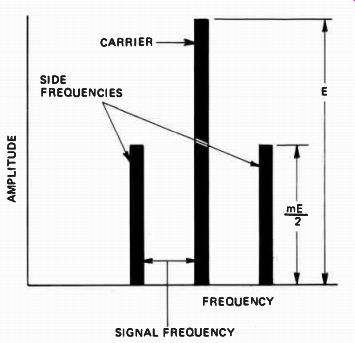
Figure 4. Relationship between carrier and side frequencies at 100%
modulation with a pure sine wave signal.
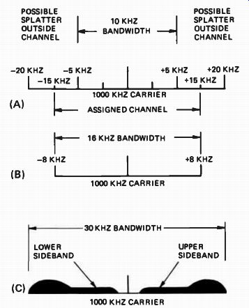
Figure 5. (A) A 1000 Hz carrier modulated with a 5 kHz wave requires
a 10 kHz bandwidth; (13) an 8 kHz modulating signal requires a 16 kHz
bandwidth. (C) The sidebands for a complex modulating signal.
To illustrate what these sidebands are, let us again use a pure sine wave as the modulating signal.
Suppose the carrier frequency is 1000 kHz and the modulating signal is 5000 Hz (5 kHz). When these signals are heterodyned in a properly-designed and adjusted class C amplifier, two new signals will be produced, one equal to the sum of the two signal frequencies which is 1000 + 5 = 1005 kHz, and the other equal to the difference between the two signal frequencies which will be 1000 - 5 = 995 kHz. The signal at the output of the modulated class C amplifier then contains three frequencies: the original carrier frequency of 1000 kHz, an upper sideband frequency of 1005 kHz, and a lower sideband of 995 kHz. These upper and lower sideband frequencies are very important because they contain all the intelligence that is in the modulated wave. The carrier signal contains none of the intelligence and can actually be eliminated as is done in some special transmitting systems.
However, in standard AM transmission it is transmitted along with the sidebands and used in the detector to extract the original modulating information. You will see how this is done later.
The strength of the upper and lower sidebands depends on the strength of the modulating sine wave signal. The higher the percentage of modulation, the greater the amplitude of the two side bands. With 100% modulation, the amplitude of each sideband is equal to one-half the amplitude of the unmodulated carrier, a ratio of 2 to 1, as shown in Fig.4. Again E is the amplitude of the unmodulated carrier. The amplitude of each side band can be computed by multiplying the values of m and E, and then dividing the product by 2. Of course, as the percentage modulation decreases, the amplitude of the sidebands also decreases.
Bandwidth. The frequencies of the upper and lower sidebands determine the bandwidth, or the space the transmitted signal occupies in the broad cast, i.e., whether the signal falls in the vhf or uhf band. As shown in Fig.5, the higher the highest frequency audio components to be transmitted, the greater the required bandwidth. To transmit a 5000 Hz (5 kHz) sine wave tone, the bandwidth must be 10 kHz; an 8000 Hz tone requires a 16 kHz bandwidth.
The waveform of a complex signal is made up of one or more fundamental frequencies and many harmonics and overtones. Therefore, when this kind of signal is used to modulate the carrier, bands of frequencies will be produced above and below the carrier, as shown in Fig.5(C). Most of the standard AM broadcast stations are assigned a bandwidth or channel 30 kHz wide, 15 kHz above and 15 kHz below the carrier. TV stations require a much wider band.
Broadcast stations are compelled by law to confine their radiation within the assigned channels. An AM broadcast station, for example, must not broadcast sideband frequencies or spurious radiations outside its channel. For example, a 5000 Hz modulated sine wave can produce spurious sidebands as much as 10 kHz, 15 kHz, or 20 kHz above and below the carrier frequency. Some of the spurious or "splatter" signals shown in Fig.5(A) will be outside the assigned channel.
There is usually a close space between broadcast stations in the frequency band. Thus, the un desirable radiation could interfere with stations transmitting on adjacent channels. However, no undesired radiation will be transmitted if the transmitter is properly designed and adjusted.
SIDEBAND POWER
When the carrier is modulated in a class C stage, the total power contained in the modulated wave at the output is the sum of the carrier power and the sideband power. The sidebands, as you have learned, contain all the intelligence. It is important for the power in the sidebands to be as high as possible to get a high signal-to-noise ratio.
Let us see how the voltage, current, and power output of the class C stage varies during modulation.
With 100% modulation, at the positive peak of the modulating cycle, the modulation envelope of the carrier is twice the amplitude of the unmodulated carrier; at the negative peak of the modulating cycle, the modulation envelope is at zero.
The average amplitude over the entire cycle, however, is equal to the amplitude of the unmodulated carrier.
Similarly, when the modulating signal is sup plied to a class C stage, although the effective value of the power input to the stage increases and decreases with the modulation, the average dc plate power input, as indicated by the panel meters, does not change. Each increase in plate voltage and plate current is followed by an equal and opposite decrease on the next half-cycle of the modulating signal. Thus, in a properly adjusted and operated transmitter, the dc plate current is always constant, with or without modulation.
Now let's see what happens to the power output of a class C stage when a modulating signal is applied to produce 100% modulation.
As you learned, power varies in accordance with the square of the current, P = I^2 R. Therefore, since the plate current on the positive peak of the modulated carrier is twice what it is for the unmodulated carrier, the power will be four times as great on the positive peak, and the average power will increase when modulation is applied.
With 100% sine wave modulation, the amplitude of each sideband is half the amplitude of the carrier. Therefore, the power in the carrier is four times the power in each sideband, or in other words, power in both sidebands is one-half the power in the carrier.
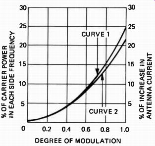
Figure 6. The effects of various degrees of modulation on the antenna
current (curve 2) and on the power in each side frequency (curve 1).
For example, if the plate input power for a stage that is unmodulated is 100 watts, then 50 watts of sine wave audio power must be added for 100% modulation. The total average input power to the transmitter, therefore, will be 150 watts.
One-third of the total average power is in the sidebands, and two-thirds is in the carrier. Thus, when 100% modulation is applied to the stage, the total power output will increase 50%. As the degree of modulation decreases, the sideband power also decreases. This is shown by curve 1 in Fig.6. At 100% modulation (m = 1), each sideband contains 25% of the carrier power; at 50% modulation (m = 0.5), each sideband contains 6% of the carrier power; and at 20% modulation (m = 0.2), each sideband contains only 1% of the carrier power.
Suppose the carrier power is 100 watts. As you learned earlier, 50 watts of modulating power must be added to modulate the carrier 100%. This can be computed in the following way, where P sb is the sideband power, P c is the carrier power, and m is the degree of modulation:
rn2 P S b = -2 X Pc 1 2 = - X 100 = 50 watts 2
For 50% modulation, the sideband power would be only 12.5 watts.
0.52 Psb = - 2 X 100 = 12.5 watts
Thus, the power in the sidebands has decreased 75% because 12.5 watts is one-quarter of the sideband power at 100% modulation (50 watts). It is the power in the sidebands alone that determines the amount of useful signal at the receiver, because only the sidebands contain the intelligence. Thus, you can see that it is very important for the carrier to be modulated as near 100% as possible to get the greatest amount of power in the sidebands.
When a complex waveform is transmitted, such as speech or music, the relationship between the power in the carrier and the power in the sidebands is not the same. The waveforms do not usually contain as much average power as is contained in the sidebands for a sine wave signal. In fact, the average power for speech is about one-half that of a sine wave. Although the average power in the sideband for speech modulation is less than with sine wave modulation, the peak of the modulating audio signal must be the same for 100% modulation.
ANTENNA CURRENT
When the carrier is modulated by a sine wave, the additional power in the sidebands causes the total power output of the transmitter to increase.
The current meters in the antenna circuits will indicate an increase in the antenna current.
Curve 2 of Fig.6 shows the percentage of increase in antenna current for different degrees of modulation. For 100% sine wave modulation, the antenna current will increase 22.5% over the unmodulated carrier value. Again this is for sine wave modulation; the percentage of increase in antenna current is less for speech or music modulation, usually from one-quarter to one-half the sine wave value.
We can also figure the increase in antenna current by rearranging the formula for power, P = I^2 R, as follows:
I = \ F P R
where I is the antenna current with an unmodulated carrier.
For example, suppose a transmitter with no modulation is supplying 100 watts to a 100-ohm antenna system. We will have: 100 = 1 amp 100 Now, if 100% modulation is added, P becomes 150 watts, and using I, for the antenna current with a modulated carrier, we have: 1, = \P 50 - 100 Ni = 1.225 amps To find the % of increase, you use the formula:
I, - I % - X 100 1 1.225 - 1 _ X 100 1
0.225 - X 100 1 = 22.5%
We can also calculate the antenna current for various degrees of modulation by using the formula: 1, As you have learned, the modulation factor, m, is 1 for 100% modulation, 0.5 for 50%, 0.2 for 20%, etc. Using the same problem we have:
I I
= Ji + 0.5 X 1
= 1.225 X 1
= 1.225 amps
As you can see this is the same figure you got using the other formula.
The percentage of increase in antenna current with sine wave modulation is a pretty good indication of the percentage of modulation. If the antenna current increases only 5%, you know you are nowhere near 100% modulation. If the increase is 20% you know you are close to 100% modulation. Final adjustments to get 100% modulation, however, are usually performed using indications other than the antenna current.
MODULATION DISTORTION
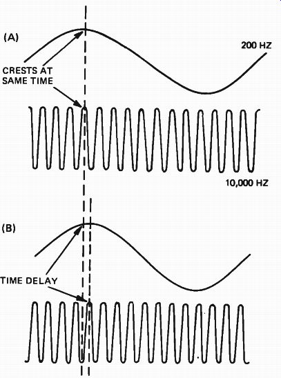
Figure 7. Phase shift between two sine waves in a transmitting system.
Any change in the modulation waveform that is not directly due to the modulating signal will introduce distortion. If the modulation signal is distorted, the sound output from a radio or the image on a TV screen will also be distorted. A distorted modulated signal can also cause spurious signal components to be radiated outside the assigned channel. Spurious radiations represent wasted power which might otherwise be used as part of the desired signal energy. Improper modulation also lowers the efficiency of the transmitter.
Let us look at some possible causes of modulation distortion.
Sideband Clipping. One source of distortion is the loss of useful sideband power when high frequency audio information is to be transmitted.
The loss of sideband energy at high modulating frequencies is often the result of insufficient bandwidth in the modulator and associated audio amplifier circuits. Poor quality audio transformers and modulation transformers can cause both high frequency and very low-frequency losses.
The Q of the tank circuit is also important to obtain the proper bandwidth. If the Q is too high, the circuit will become too selective, and some of the useful sidebands may be cut off or clipped.
Too low a Q circuit is also undesirable. A low Q circuit is difficult to load properly. This will also influence the bandwidth. Likewise, proper matching of the transmission line system to the antenna is an important consideration. Bandwidth is especially important when it is necessary to convey the very wide band of frequencies required in the transmission of a television signal.
Phase Shift. An improper phase shift in the audio amplifier, modulator, or modulated amplifier can cause a particular type of audio distortion.
Phase shift causes a nonuniform time delay of various audio components. For example, let us assume that the crest of a 200 Hz sine wave and a 10,000 Hz sine wave occur at the same instant during the pickup of a particular program.
This is shown by the waveform in Fig.7(A). No attempt has been made in the diagram to show the exact frequency ratio between the two waveforms.
If phase shift is present in the transmitting signal, the peak of the 10,000 Hz tone as reproduced at the receiver loudspeaker will be time-displaced with respect to the reproduction of the peak of the 200 Hz tone. In other words, the 10,000 Hz tone will reach its crest after the crest of the 200 Hz tone as shown in Fig.7(B). The sound from the loudspeaker will be blurred.
Phase shift in audio systems can be caused by inadequate amplifier frequency response, mis matches, incorrectly designed filters and compensators, and improper bandwidth of the modulated class C amplifier or antenna system. The problems of phase shift are also magnified in television modulating systems, and especially in the transmission of a color picture. This type of distortion is difficult to correct; it can be prevented only by proper design of the signal amplifiers and modulators.
Overmodulation. As you know, overmodulation occurs when the transmitter modulation is over 100%. When this happens, one side of the modulated signal becomes compressed. This not only causes distorted audio output at the receiver, but also produces sidebands that can interfere with stations on adjacent channels.
When a standard AM broadcast band transmitter is modulated correctly, the reading on the dc plate current meter will not vary. However, if the transmitter is over-modulated, the reading on the meter will vary, instead of remaining constant as it should. The way to remedy overmodulation is to decrease the degree of modulation. However, in most transmitters, there are circuits that are designed to limit the peak amplitude of the modulating signal and thus prevent over modulation.
Carrier Shift. Another type of distortion is called carrier shift. With this type of distortion, the modulated signal is asymmetrical. In other words, the amplitude of the positive and negative modulation peaks are not the same. Carrier shift can be either positive or negative as shown in Fig.8(C) and (D). Let us see what happens in each case.
As you have learned, in a class C stage with 100% or less modulation, the average plate current is the same as with no modulation. However, if the modulation is not symmetrical, the average plate current will vary. If the negative part of the modulation is greater than the positive as shown in Fig.8(C), there is a decrease in the average power output and a decrease in the plate current drawn by the stage. This is called negative carrier shift. It is quite easily detected by watching the plate current meter on the modulated stage. As the stage is modulated, the meter will kick down slightly.
If the positive part of the modulation is greater than the negative, as shown in Fig.8(D), there is an increase in the average power output, and an increase in the plate current; this is called positive carrier shift. It can be detected by an upward kick in the plate current meter reading as the carrier is modulated.
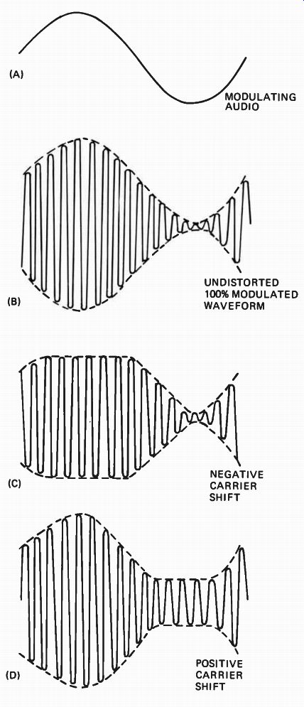
Figure 8. Result of carrier shift on modulation envelopes.
Negative carrier shift may be due to a distorted modulating wave from the modulator and its audio system; overmodulation; improper matching between modulator and modulated stage; an improperly tuned class C stage; insufficient radio frequency excitation to the modulated stage; or poor power supply regulation of the modulator or modulated stage. Positive carrier shift is most often caused by parasitic oscillations, incorrect neutralization, or incorrect bias. It can also be the result of improper tuning or loading of a class C stage, or distortion of the modulating signal.
Almost any type of asymmetrical modulation can cause carrier shift. If the asymmetrical modulation is the result of an asymmetrical modulating signal, the defect is in the modulator or its associated audio amplifier chain. The asymmetrical modulation can also be caused by a defect that arises in the actual modulation process, such as parasitic oscillations, incomplete neutralization, or the inability of the power output of the class C stage to follow the modulating wave. In other words, incorrect tuning, insufficient excitation, incorrect bias, or inability of the power supply to furnish the necessary current on modulation peaks can cause distorted modulation even though the applied modulating signal is not distorted.
It is quite important that you remember what carrier shift is, and know how to identify both positive and negative carrier shift. You should also know the causes of each type so that when you run into it you will be able to remedy it. Also, you can be pretty sure when you go for your FCC License Examination that there will be one or more questions on carrier shift.
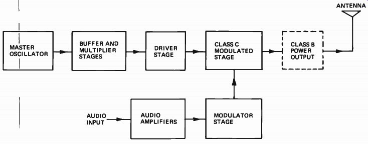
Figure 9. Block diagram of a typical amplitude-modulated transmitter.
AMPLITUDE-MODULATION SYSTEMS
In an AM transmitter, the carrier signal is generated in the master oscillator and amplified class C amplifier stages. These stages are shown in Fig.9. The audio signal from a microphone or other signal source is amplified in the audio amplifier stages and the modulator, and it is then applied to the class C power amplifier. This is the stage in which the mixing or heterodyning of the two modulation signal components (the carrier and the audio) takes place.
In low-power transmitters, the plate of the final or power output stage is usually modulated, and the modulated signal is fed directly to the transmitting antenna. This is called "high-level" modulation.
More powerful transmitters have additional power amplifiers following the modulated stage. This is called "low-level" modulation.
When the transmitter is used for voice, music, or TV signals, the following amplifier must be operated either in class A or class B (usually class B as in Fig.9) because it gives a higher power output.
Sometimes you will find beam power tetrodes operated in class AB in this type of stage. A class C stage cannot be used; it will distort the modulated signal waveform. An exception to this is the system that combines phase modulation and amplitude modulation. You will learn about it in a later lesson.
The primary requirement of the modulator stage is to produce an undistorted output signal at a high enough power level to modulate the carrier properly. The modulator stage in a transmitter is basically a high-powered audio amplifier, operated in class A or class B. You have studied audio amplifiers earlier, so we will not give a complete discussion of this circuit here. We will be concerned with the operation of the modulated class C stage and the methods used to modulate the rf carrier signals.
There are a number of ways that you can amplitude modulate a class C stage. Two of these are: plate modulation when a vacuum tube is used, and collector modulation when a transistor is used.
We will discuss these two types in the next two sections of the lesson and then other types of modulation that you might encounter in a following section.
SELF-TEST QUESTIONS
1 What is the simplest form of modulation?
2 What type of modulation is used in the standard radio broadcast band?
3 If the output power in the carrier of a standard broadcast station is 1000 watts with no modulation, what will the power be with 100% modulation?
4 If the modulation index is 0.5, what is the percentage of modulation?
5 What is the minimum bandwidth required in AM modulation to transmit a 15 kHz audio tone?
6 If the unmodulated power in a carrier is 100 watts, what will the power be in one sideband with 50% modulation?
7 If the antenna current of a transmitter is 10 amps with no modulation, and it increases to 11 amps with modulation, would you say that the modulation is 100% or less than 100%?
8 If when you modulate a transmitter the plate current of the modulated stage kicks upward, what does this indicate?
-------
Plate Modulation
Plate modulation can be used in a class C amplifier stage using vacuum tubes because of the relationship between the plate voltage and power output. Changing the plate voltage changes the mutual conductance of the tube. When the plate voltage is doubled, the power output will increase four times. This output variation, with variations in plate voltage, provides linear amplitude modulation.
A basic plate-modulation system is shown in Fig.10. The modulating audio signal is inserted, by means of the modulation transformer, in series with the plate-supply line. Variations in the audio voltage add to and subtract from the dc voltage applied to the plate of the class C stage. In this way the rf carrier applied to the grid of the modulated stage and the audio variations on the plate are mixed in the tube to produce the modulated output waveform. To get 100% modulation, the highest amplitude audio component must be able to vary the class C plate voltage from approximately zero to twice its normal unmodulated dc value.
An undistorted sine wave signal will cause the plate voltage to increase and decrease the same amount, so the average dc plate voltage and plate current remain constant. In other words, the reading on the dc plate current meter in the class C stage should remain constant and have the same value as for the unmodulated carrier. Any variation in the dc plate current with modulation indicates improper adjustment or a circuit defect.
As you have learned, for 100% modulation of a class C stage, the power of the modulating signal must be 50% of the carrier power. This means that the modulator must add audio power to the stage equal to one-half the dc plate input power. This increases the power input to the stage, and therefore increases the plate dissipation. The stage must be designed so that the plate dissipation rating of the tube is not exceeded. This means that with no modulation the plate dissipation should be only two-thirds of the maximum rated plate dissipation of the tube. Thus, when the input power to the stage increases 50% with 100% modulation, the peak plate dissipation will be equal to the maximum rated plate dissipation of the tube.
The modulation transformer must act as an impedance-matching device between the plate out put impedance of the modulator and the plate input impedance of the modulated stage.
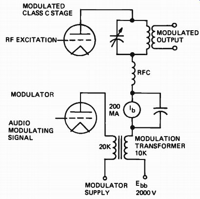
Figure 10. Basic plate-modulation system.
The plate input impedance of the modulated stage can be found by dividing the plate supply voltage by the dc plate current in amperes. For example, suppose that the plate supply voltage (Eb b) of a class C modulated stage is 2000 volts, and the dc plate current (l b) is 200 ma (0.2 amp)
as in Fig.10. The impedance (Zs) would be:
Z = s Ib 0.2 b b = E 2000 10,000 ohms
If we find from a tube manual that the modulator must have a load impedance of 20,000 ohms, we can find the turns ratio, n, of the modulation transformer as follows, where Zp is the primary impedance and Z s is the secondary impedance:
n \s/Zp \/20,000 _ 1.4 V 2 = z s 10,000
Thus the primary of the transformer must have 1.4 times as many turns as the secondary.
Now let us find the power required to modulate the class C stage. The formula for finding the input power, P in , of the class C stage is:
Pin - Ebb X lb
so we have: Pi ll = 2000 X 0.2 = 400 watts
The maximum power required from the modulator (Pm ) is half of the carrier power for 100% modulation, and we have: P i n P m = = 200 watts 2
This makes a total of 600 watts of input power in the class C modulated stage on modulation peaks when 100% modulation is reached. If we know the efficiency of the modulated stage, we can find the output power, P o: P. = efficiency X input power If the efficiency of this stage is 70% when no modulation is applied, we would have: P o = 0.7 X 400 = 280 watts
With 100% modulation, we would have: P o = 0.7 X 600 = 420 watts
A PLATE-MODULATED TRIODE
A triode tube can be plate-modulated 100% by using the circuit shown in Fig. 11. The modulator in this circuit is a push-pull class B stage. The output of the modulator is transformer-coupled into the plate supply circuit of the class C rf amplifier stage. The audio voltage developed across the secondary of the transformer adds to and subtracts from the plate supply voltage for the modulated stage. This changing plate voltage, when applied to the class C amplifier, forms a modulated rf output.
The dc component of plate current for the modulated stage flows through the secondary of the modulation transformer T2, the meter Ml, and the rf choke. The choke is used to block the rf energy from the metering circuit, the modulator, and the power supply. The rf choke in no way impedes the audio signal because its reactance is extremely low at audio frequencies. A small capacitor shunts the dc plate current meter to provide a low impedance rf path around the meter.
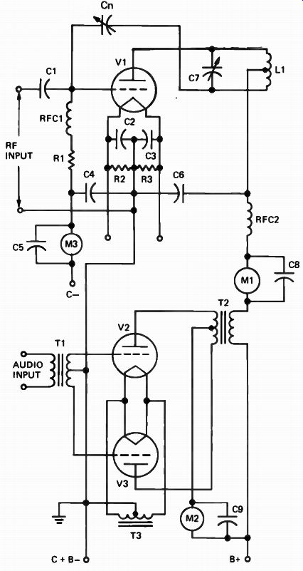
Figure 11. A plate-modulated class C triode rf amplifier.
The class C modulated stage is a plate neutralized triode. The supply voltage and modulation are applied to the plate circuit at the tap on the tank circuit coil, L1. The tube shown is a filament type. Notice in the filament circuit that a true ground point for low frequencies as well as radio frequencies is obtained with a center-tapped connection to a pair of capacitors and resistors shunted across the filament line. This method of connection prevents the ac-powered filament circuit from hum modulating the carrier.
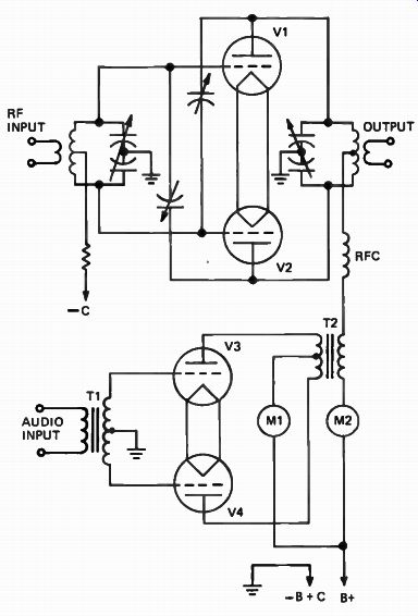
Figure 12. Push-pull zero bias class B modulator and push-pull output.
Grid bias is obtained by using a combination of external and grid leak bias. The rf amplifier must self-bias itself somewhat to prevent excessive grid current during the time the modulation drives the plate voltage to very low values. An increase in the grid current flow through resistor R1 automatically causes an increase in the grid bias, which stabilizes the grid circuit. The grid leak arrangement also improves the linearity of the circuit by preventing the grid from robbing the plate of electrons during the modulation troughs. The plate current can then follow the plate voltage variations more closely.
PLATE-MODULATED PUSH-PULL STAGE
Another circuit using plate modulation is shown in Fig.12. This circuit uses a push-pull class B modulator stage, which is transformer-coupled to the plate circuit of the push-pull class C stage.
Notice that there is no bias on the modulator stage.
This is because the tubes used in this stage are a special type of zero bias tube. They are designed and built so that with zero bias applied to them there will be little or no plate current flow through the tube. Thus the tubes operate in class B without any external bias; this eliminates the need for a special bias supply for the class B modulator.
Notice also that in the circuit shown in Fig.12 (and Fig.11 also) the supply lines to the class B and class C modulator amplifiers are metered separately. With modulation, the class C plate current should remain constant, indicating symmetry of modulation. However, from your knowledge of class B operation, you can expect that the plate current meter for the modulator will fluctuate with the audio information. This is normal. In fact, with the class B stage biased to near cutoff, as required, the plate current reading will be nearly zero with no modulation. The meter reading will increase with modulation - the greater the amplitude of the modulation, the higher the meter reading.
The connection for the high-voltage plate voltage for the class C stage is through the meter M2, the secondary of the modulation transformer, the rf choke, and to the center tap of the tank circuit coil. Notice that a bypass capacitor need not be connected from the center tap of the rf coil to ground because of the balanced split-stator circuit and the fact that the center tap of the capacitor is at rf ground potential. As a result, the high-frequency audio signals are not bypassed by a capacitor as they are by capacitor C6 in Fig.11. A split-stator capacitor is one with two separate stators and a common rotor.
TETRODE OR PENTODE PLATE MODULATION
You will remember that there is a linear relationship between the plate current and the plate voltage in a triode tube. By this we mean that if you double the plate voltage, the plate current will double. This is a requirement that must be met for linear modulation. When we modulate a triode 100% and double the plate voltage, the plate current doubles so that we have four times the peak power output. This happens because the plate current for triode tubes depends primarily on the plate voltage.
To obtain 100% plate modulation of a tetrode or pentode tube, both the plate voltage and the screen voltage must be modulated. The reason for this is that the plate current in a tetrode or pentode does not primarily depend upon the plate voltage, but rather on the screen voltage. There fore, in order to double the plate current of a tetrode or pentode, when we double the plate voltage we must also double the screen voltage.
Similarly, to drive the plate current to cutoff we must drive the screen voltage essentially to zero.
There are several methods used to produce simultaneous changes in the plate and screen voltage of tetrode and pentode tubes. Three of the most widely used methods are shown in Fig.13.
In Fig.13(A) we have shown a circuit using a modulation transformer, TI, with two secondary windings. The voltage developed in one winding is used to modulate the screen, and the voltage developed in the other is used to modulate the plate. Thus both the screen and plate voltages are varied by the modulating signal. This circuit is often used to modulate high-power tetrode class C amplifiers. With this type of arrangement, both secondaries must have the correct number of turns.
In other words, it is not sufficient simply to have the plate circuit of the class C stage matched to the plate circuit of the modulators; the screen circuit must also be matched. Thus a rather carefully designed and frequently quite expensive modulation transformer is required for this arrangement.
Another circuit used with high-power class C stages is shown in Fig.13(B). Notice that in this circuit the plate supply voltage from the class C stage is fed through the secondary of the modulation transformer. There is no connection from the modulation transformer to the screen. The screen voltage is supplied to the screen of the tube through the audio choke L1. This choke has a high impedance at audio frequencies.
The success of this system depends on the fact that the plate will attract many more electrons when the modulating signal causes the plate voltage to increase above the no-modulation level. When the plate voltage increases, the plate begins attracting electrons that would normally flow to the screen. This causes the screen current to drop.
The change in screen current induces a voltage in the choke L1 that is in series with the screen supply voltage. Thus the screen voltage increases when the plate voltage increases. The increase in screen voltage causes the plate current to increase
This is because the tubes used in this stage are a special type of zero bias tube. They are designed and built so that with zero bias applied to them there will be little or no plate current flow through the tube. Thus the tubes operate in class B without any external bias; this eliminates the need for a special bias supply for the class B modulator.
Notice also that in the circuit shown in Fig.12 (and Fig.11 also) the supply lines to the class B and class C modulator amplifiers are metered separately. With modulation, the class C plate current should remain constant, indicating symmetry of modulation. However, from your knowledge of class B operation, you can expect that the plate current meter for the modulator will fluctuate with the audio information. This is normal. In fact, with the class B stage biased to near cutoff, as required, the plate current reading will be nearly zero with no modulation. The meter reading will increase with modulation--the greater the amplitude of the modulation, the higher the meter reading.
The connection for the high-voltage plate voltage for the class C stage is through the meter M2, the secondary of the modulation transformer, the rf choke, and to the center tap of the tank circuit coil. Notice that a bypass capacitor need not be connected from the center tap of the rf coil to ground because of the balanced split-stator circuit and the fact that the center tap of the capacitor is at rf ground potential. As a result, the high-frequency audio signals are not bypassed by a capacitor as they are by capacitor C6 in Fig.11. A split-stator capacitor is one with two separate stators and a common rotor.
TETRODE OR PENTODE PLATE MODULATION
You will remember that there is a linear relationship between the plate current and the plate voltage in a triode tube. By this we mean that if you double the plate voltage, the plate current will double. This is a requirement that must be met for linear modulation. When we modulate a triode 100% and double the plate voltage, the plate current doubles so that we have four times the peak power output. This happens because the plate current for triode tubes depends primarily on the plate voltage.
To obtain 100% plate modulation of a tetrode or pentode tube, both the plate voltage and the screen voltage must be modulated. The reason for this is that the plate current in a tetrode or pentode does not primarily depend upon the plate voltage, but rather on the screen voltage. There fore, in order to double the plate current of a tetrode or pentode, when we double the plate voltage we must also double the screen voltage.
Similarly, to drive the plate current to cutoff we must drive the screen voltage essentially to zero.
There are several methods used to produce simultaneous changes in the plate and screen voltage of tetrode and pentode tubes. Three of the most widely used methods are shown in Fig.13.
In Fig.13(A) we have shown a circuit using a modulation transformer, TI, with two secondary windings. The voltage developed in one winding is used to modulate the screen, and the voltage developed in the other is used to modulate the plate. Thus both the screen and plate voltages are varied by the modulating signal. This circuit is often used to modulate high-power tetrode class C amplifiers. With this type of arrangement, both secondaries must have the correct number of turns.
In other words, it is not sufficient simply to have the plate circuit of the class C stage matched to the plate circuit of the modulators; the screen circuit must also be matched. Thus a rather carefully designed and frequently quite expensive modulation transformer is required for this arrangement.
Another circuit used with high-power class C stages is shown in Fig.13(B). Notice that in this circuit the plate supply voltage from the class C stage is fed through the secondary of the modulation transformer. There is no connection from the modulation transformer to the screen. The screen voltage is supplied to the screen of the tube through the audio choke L1. This choke has a high impedance at audio frequencies.
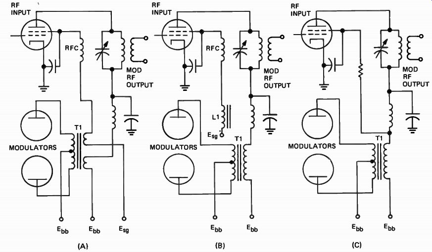
Figure 13. Methods of modulating plate and screen grid of tetrode
or pentode tube.
The success of this system depends on the fact that the plate will attract many more electrons when the modulating signal causes the plate voltage to increase above the no-modulation level. When the plate voltage increases, the plate begins attracting electrons that would normally flow to the screen. This causes the screen current to drop.
The change in screen current induces a voltage in the choke LI that is in series with the screen supply voltage. Thus the screen voltage increases when the plate voltage increases. The increase in screen voltage causes the plate current to increase still further. When the modulating signal reverses polarity and reduces the plate voltage on the tube, the plate will attract fewer electrons. This means that there will be more electrons available to flow to the screen so the screen current will increase.
The increase in current through L1 will induce a voltage in L1 which opposes the screen voltage supply so that the screen voltage decreases. When the screen voltage decreases, the plate current will decrease still further.
A third method of modulating the screen is shown in Fig.13(C). Here the screen voltage is fed through a series resistor from the modulated plate supply voltage. Thus if the plate voltage varies, the screen voltage will also vary because the voltage to the screen circuit varies. The big disadvantage to this system lies in the fact that in big tetrode tubes the screen voltage is usually much lower than the plate voltage. In a tube that operates with a plate voltage of 2000 volts, the screen voltage may be as low as about 400 volts. Thus we would have to drop and waste 1600 volts in the screen-dropping resistor. This scheme can be used in low-power tetrode stages, but it is too wasteful to use in high-power stages.
If a class C stage using a multigrid tube is plate modulated alone, there is a nonlinear relationship between the plate voltage and the power output because the plate current does not vary linearly with the plate voltage. The modulation is com pressed in the high-amplitude ranges before 100% modulation can be reached. Thus a compressed and distorted modulation envelope is produced.
HEISING MODULATOR
An older and seldom used type of modulation is the Heising system shown in Fig.14. In fact, you could probably forget about this type of modulator completely except that questions frequently appear about it on the FCC License Examination.
In the Heising modulator, the audio information is developed across coil L1 through which the class C stage also receives its voltage. The plate supply current divides between the modulator and the class C stage in such a way that the audio voltage developed across L1 adds to and subtracts from the supply voltage. This varies the plate voltage to the class C amplifier.
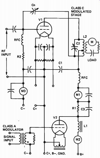
Figure 14. The Heising or "constant-current" method of plate
modulating a class C amplifier.
One advantage of the Heising system is that the same power supply can be used for both the modulator and the modulated amplifier. To get 100% modulation, the plate current drawn by the modulator should vary between 0 and an extremely high value. However, you cannot operate a class A amplifier stage this way and obtain a linear output. Consequently, the class C amplifier must be operated with a plate voltage 30 to 40% lower than the modulator plate voltage. With this reduced voltage and high enough variation in the audio output, voltage of the modulator can be obtained to reach 100% modulation. Resistor R1 acts as a voltage-dropping resistor and reduces the dc plate voltage supplied to the modulated stage.
Capacitor C3 bypasses the audio modulating signal around the resistor.
This modulation system is undesirable except in very low power equipment because of the large amount of power lost in the resistor. Furthermore, it is not practical to try to develop large amounts of audio power with a class A amplifier.
ADJUSTING A PLATE-MODULATED Amplifier
The initial adjustment procedure for a modulated class C amplifier is the same as for a non-modulated (cw) class C amplifier. With the modulator turned off (no audio being fed to the class C stage), go through the neutralizing, grid excitation, and plate tuning and loading procedures as recommended by the transmitter manufacturer.
Make sure that the plate voltage and current, the excitation, and the grid bias are correct.
It is important that the excitation be adjusted correctly to get linear modulation. Insufficient excitation can reduce the amplifier efficiency and the power output, produce overmodulation, and cause negative carrier shift.
Increase the excitation until there is no further increase in the antenna current. Then, decrease it slightly to see if there is an immediate decrease in the antenna current. When the excitation is set correctly, there will be a slight increase and decrease in antenna current when you vary the excitation slightly. This adjustment makes certain that the class C stage is driven into saturation.
The plate voltage and plate current must be set to rated values because they determine the impedance into which the modulator must work - the impedance that the modulator was designed to match. The antenna coupling must be adjusted so that, with the plate circuit tuned exactly to resonance, the plate draws the rated current.
The next step is to adjust for 100% sinusoidal modulation. You can do this by feeding an audio signal from an audio oscillator to the modulator input. The audio signal must have an amplitude equal to the signal that will normally be fed to the modulator. Increase the gain of the modulator until the antenna current rises slightly less than 22.5%; the stage is then modulated close to 100%. You should then use a modulation monitor, which we will discuss later, to make the final modulation adjustment for maximum modulation.
As you increase the modulation to bring the modulation level close to 100%, there should be no change in the class C modulated amplifier dc plate current. Any variation in this plate current reading indicates a carrier shift and a nonsymmetrical modulation characteristic.
One type of rf current meter used to measure antenna current uses a device called a thermo couple. This type of meter depends on the current flowing through the thermocouple producing heat which in turn generates a voltage which causes the meter to operate. When this type of rf meter is used in the antenna circuit, the heat produced by the current flowing through the thermocouple must become stable before the meter pointer will come to rest. Time is required to heat the junction and generate the voltage to operate the meter.
Therefore, a thermocouple meter does not respond immediately to changes in circuit adjustments; the adjustments must be made slowly to compensate for the lag in the meter itself.
COLLECTOR MODULATION
Class C transistor rf power amplifiers can be modulated using methods similar to plate modulation for vacuum tubes. The solid-state equivalent of plate modulation is collector modulation.
Most AM transmitters that you are likely to run into will be fairly high-powered units and in most cases will use vacuum tubes rather than transistors. Therefore you are not likely to run into too many transistorized modulated-amplifiers except in the case of low-power equipment such as citizens band equipment, portable equipment for police or emergency work, or amateur equipment.
However, you should know how a transistor amplifier can be modulated. You should be familiar with this type of equipment because you may have to repair some citizens band equipment or other low-power equipment using transistors at some time.
Transistor Characteristics. You will remember from your earlier study of transistors that the characteristic curve showing the collector voltage against collector current in many respects resembles the characteristic curve of the plate voltage versus plate current for a tetrode or a pentode tube. There is not a linear relationship between collector voltage and collector current. By that we mean that if you double the collector voltage, the collector current will not double; as a matter of fact, in some instances it will increase very little.
Because of this nonlinear relationship between collector voltage and collector current, modulating the collector alone will not produce distortion-free amplitude modulation. We would run into a situation similar to that encountered in a tetrode or pentode tube where only the plate is modulated.
The modulation would be compressed at high volume levels.
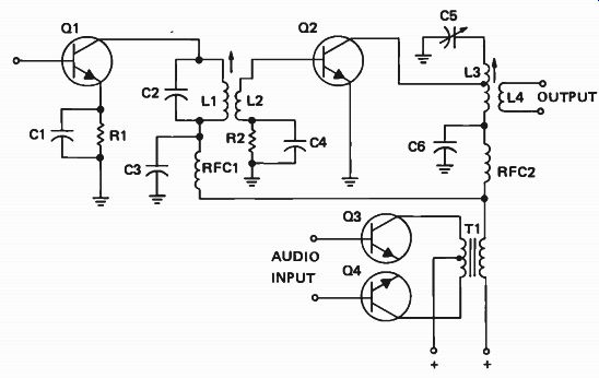
Figure 15. A collector-modulated amplifier.
A Typical Collector-Modulated Amplifier.
Figure 15 is a schematic diagram showing how collector modulation of a transistor amplifier is accomplished. Notice that the if input is fed into the base of Q1. In the collector circuit of Q1 we have a parallel-resonant circuit consisting of L1 and C2. L1 is inductively coupled to L2 so the rf signal is induced in L2 and applied between the base and ground of Q2. Q2, the final rf power amplifier, is connected to the rf output tank circuit consisting of L3 and C5.
In order to obtain 100% collector modulation we modulate both the collector of Q1 and the collector of Q2. Modulating the collector of Q1 will produce some amplitude modulation of the rf signal at the output of Q1. This signal in turn is fed to the base of Q2 resulting in considerable change in the base current with the amplitude-modulation variations. This will produce the change in collector current. The modulation is also applied to the collector of Q2 and this, along with the partially modulated rf carrier which is fed to the base of Q2, results in reasonably effective collector modulation.
In the modulator we have shown push-pull transistors feeding a modulation transformer with a center-tapped primary. In some circuits a single ended push-pull arrangement might be used and in this case the primary of the modulation trans former probably would not be tapped.
In some applications applying the modulation directly to the collector of Q1 may result in overmodulation. In this case, the amount of modulation fed to the collector of Q1 can be controlled by replacing the rf choke RFC1 with a resistor. This would reduce the dc voltage and also the modulated voltage fed to the collector of Q1.
It will also reduce the amplitude of the partially modulated signal fed to the base of Q2. However, usually it is not necessary to do this. Simply adjusting the level of the audio gain correctly in the audio amplifier will provide the correct amount of voltage at the output to produce 100% modulation without overmodulation.
SELF-TEST QUESTIONS
9 When the plate voltage on a triode tube is doubled, what happens to the power output?
10 What must the turns ratio be on a modulation transformer if the class C stage is operated at 1000 volts and draws a plate current of 125 ma and the modulator stage requires a plate to-plate impedance of 16,000 ohms?
11 Why are the tubes in the push-pull class B modulator shown in Fig.12 operated with no bias?
12 Why can we not obtain 100% modulation of a tetrode or pentode tube by modulating the plate alone?
13 Why is the screen modulation arrangement shown in Fig.13(C) not practical in high power class C amplifiers?
14 What is the disadvantage of Heising modulation?
15 What characteristic of a transistor makes it impossible to obtain 100% modulation if only the collector is modulated?
16 How is 100% collector modulation obtained?
---------------------------------------
Grid Modulation Systems
The modulation in an amplitude-modulation system using vacuum tubes can be applied to the control grid of the modulated stage instead of the plate. These two forms of amplitude modulation, plate modulation and grid modulation, are the most common.
However, a class C amplifier can also be modulated in other ways. Stages using multigrid tubes can be modulated by applying the modulating signal to the screen grid or the suppressor grid. In this section we will take up control-grid modulation first, then we will study screen-grid and suppressor-grid modulation. Another form of grid modulation that we will study is called "suppressed-carrier" modulation. We will also study transmitter-keying, which is usually done in the grid circuit.
CONTROL-GRID MODULATION
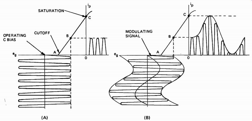
Figure 16. Grid modulation waveforms.
In a control-grid modulation system, the plate input power and the rf grid excitation are constant.
The modulation is applied to the control-grid circuit.
The rf stage used for grid modulation is not truly class C, but is biased somewhere between class B and class C. Figure 16(A) shows the tube characteristic curve and the waveforms with no modulation. Notice that the peak plate current drawn is at the center of the linear portion of the curve, point B. The modulating voltage is superimposed on the fixed grid bias, and the effective grid voltage varies with the modulating signal. The amplitude of the modulating signal is chosen so that the limit of modulation extends over the linear part of the curve, between points A and C. This is shown in Fig.16(B). The plate current pulses that excite the tank circuit also vary in peak amplitude according to the modulation. As a result, a modulation envelope is formed in the tank circuit; the tank circuit voltage and the power output follow the modulating signal variations.
The rf excitation must be adjusted so that when it is 100% modulated, at the crest of the modulation, the rf cycles reach up to the saturation point (C in Fig.16) but do not go beyond it.
As you can see, the settings of the grid excitation, the amplitude of the modulating signal, and the grid bias are important for linear and efficient grid modulation. If the excitation is excessive, the dc plate current will vary.
The efficiency of a grid-modulated amplifier when no modulation is being applied is approximately half that of a plate-modulated amplifier - approximately 35%. However, when 100% modulation is applied, the positive alternations of the excitation reach up nearly to saturation, and therefore the efficiency rises to nearly 70%. This rise in efficiency is the extra power necessary to form the sidebands of the modulated signal. In plate modulation, the power for the sidebands is supplied by the modulator; in grid modulation, this extra power is provided by the rise in efficiency with modulation. For this reason, all forms of grid modulation are frequently referred to as efficiency modulation.
The maximum output with grid modulation is much less (approximately one-quarter) than that obtainable when using the same tube with plate modulation. The major advantage of grid modulation is that less modulator power is required than for plate modulation. With grid modulation, the modulated stage itself supplies the sideband power; the audio signal on the grid changes the efficiency of operation. Thus, the power required from the modulator is very small. For example, it is possible to modulate a 1000-watt carrier fully with as little as 20 watts of audio power. A bulky, expensive, and high-powered modulation system is not required.
To get the least distortion in a grid-modulated system, the modulator and driver must have good regulation, so that they will supply the necessary driving energy as the grid impedance of the modulated stage changes throughout the modulation cycle. Generally the grid input circuit is loaded or a limit is placed on the amount of grid current. Then the input impedance variations are not as great as when the stage is operated as an unmodulated class C amplifier. Figure 17 shows a grid modulation circuit. In this circuit, the output of the modulator is loaded by resistor R1 to maintain a more constant load on the modulator.
In practice the exciter and the modulator are designed to deliver two or three times as much power as is necessary so that the modulating system can be loaded and thus give more favorable regulation.
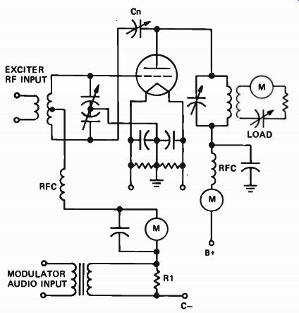
Figure 17. Circuit for grid modulation.
Adjustments. When tuning a grid-modulated amplifier, you must first run through the same preliminary steps as for tuning an unmodulated class C stage. After you have made these preliminary adjustments, you must set the class C bias, the rf grid excitation, and the loading presented by the output tank circuit to get a linear modulation characteristic.
One method of adjusting the grid circuit is to set the class C bias (with no rf excitation applied) to a value that just begins to draw plate current when the plate voltage is set to the recommended value. As you increase the excitation, watch the meter reading for the plate current and the antenna current. Increase the excitation until the plate current continues to rise sharply but there is no further proportional increase in the antenna cur rent reading. At this point, the class C stage is being driven to the saturation level and the output is maximum. This is the level of operation that represents the crest of 100% modulation.
Increase the grid bias until the antenna current is reduced to half the peak value. This step will increase the bias the proper amount to allow the crest of the unmodulated carrier to occur at the center of the linear portion of the transfer characteristic, point B of Fig.16. The dc component of the plate current should also be at the recommended value. If it is not, a loading adjustment must be made so that the proper load is being presented to the tube.
With the operating voltages and currents set correctly, if a sine wave signal is fed to the audio system to modulate the class C stage, and the antenna-current meter has increased 22.5% above its "no modulation" value, you have 100% modulation. Additional information on modulation adjustments will be given when you study modulation monitors.
Distortion. Some causes of carrier shift are poor regulation of the rf exciter and distortion in the modulator and associated amplifiers. Proper loading of the tank circuit is important because the most linear modulation is obtained when the tube works into a rather high value of tank circuit impedance. The output coupling must be adjusted until 100% modulation can be obtained without carrier shift.
Two of the causes of downward modulation in a grid-modulated stage are too low an operating bias and excessive rf grid excitation. Poor power supply regulation, improper loading of the class C tube, or a defective tube itself can also be suspected.
SCREEN AND SUPPRESSOR-GRID SYSTEMS
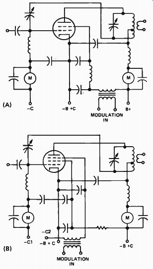
Figure 18. Typical circuits for (A) screen and (B) suppressor modulation.
A class C amplifier stage using a tetrode tube can be modulated by applying the modulating signal to the screen of the tube. A class C amplifier stage using a pentode tube can be modulated by applying the modulating signal to either the screen grid or the suppressor grid, as shown in Fig.18.
Suppressor-grid and screen-grid modulation systems, however, cannot be modulated to 100% because voltage changes on these elements do not have a linear effect on the plate current. The limit of undistorted modulation is about 80%. A few special tubes that have been designed for this type of modulation can reach 100% modulation without serious distortion. The carrier efficiency of both types of modulation is approximately 35%, about the same as for control-grid modulation.
Screen-Grid Modulation. In a screen-grid modulated system, a modulating signal voltage is used to vary the screen-grid voltage of the modulated stage.
The dc screen voltage must be adjusted so that at the peak of the modulation it will be the same as that for a stage operating as a class C amplifier without modulation. Therefore if the stage is to be screen modulated, the dc screen voltage supplied is usually about half the rated value for normal operation. The modulating signal then varies the screen voltage between zero on the modulation troughs and the rated value on the peaks.
The modulating power required for screen-grid modulation is slightly more than is required for control-grid modulation. However, there is less distortion on the peaks of the modulated signal because the load presented by the modulated stage to the modulating voltage does not vary with the signal-voltage variation. In some circuits, part of the modulation voltage is applied to the screen grid of the driver stage. This is done to permit a higher modulation percentage without distortion.
Suppressor-Grid Modulation. The suppressor grid of a receiving-type pentode tube is generally connected directly to the cathode so that the potential between the cathode and suppressor is zero. The suppressor grid of a transmitting tube is usually operated at zero voltage also, but some times it is operated with either a small positive or a small negative voltage applied to it.
In the suppressor-grid modulation system, the suppressor grid is operated with a negative voltage applied to it. The modulation signal, which is fed to the suppressor grid in series with the negative voltage, varies the voltage on the suppressor grid.
This, in turn, causes the plate current to vary. The negative bias on the tube and the modulation signal are adjusted so that the plate current is swung from zero to the rated value for the tube when it is operated as a class C amplifier without modulation.
The power required to modulate this stage is very low, about the same as required for control-grid modulation. At the modulation peaks, the power output is about the same as for a normal class C stage, but the overall efficiency of the system is about the same as for a grid-modulated signal.
Adjustments. The adjustments that you will normally have to make on either a screen-grid or a suppressor-grid modulator are quite simple. The most important thing is to get the class C stage operating correctly first. The transmitter manufacturer will supply information on what the plate current of the final stage should be. You should load the transmitter to get the rated plate current and then feed a sine wave signal to the input and adjust the gain of the modulator to give as near 100% modulation as possible without distortion.
The modulated output should be checked with a cathode-ray oscilloscope. You will learn how to do this later. If you detect any nonlinearity you may find an adjustment that can be used to vary the screen voltage on a screen-modulated stage or the suppressor voltage on a suppressor-modulated stage. Varying this voltage may enable you to improve the linearity. We will go into nonlinearity in a later lesson on oscilloscopes.
SUPPRESSED-CARRIER SYSTEMS
In the modulation systems we have discussed so far, the modulated signal, composed of both the carrier and the sidebands, was fed to the transmitting antenna. It is also possible to remove the carrier completely from the transmitted signal and transmit only the sidebands because all of the information being transmitted is contained in the sidebands. This is called suppressed-carrier modulation. The carrier must be added again by a low-powered local generator in the receiver itself for demodulation. The inserted carrier takes the place of the carrier that is removed by the suppressed-carrier modulation system.
The basic circuit for a suppressed-carrier sys tem is shown in Fig.19. This system uses grid modulation. The modulated stage has two tubes, and the grids of the two tubes are excited out of phase by the modulating information. Two transistors could be used in place of the tubes, but the circuit would be essentially the same.
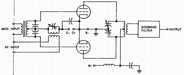
Figure 19. Circuit for suppressed--carrier single--sideband circuit.
The rf carrier signal is fed to a center tap on the grid-modulation transformer so that the grids receive the rf signal in phase. The plates are connected in push-pull.
Since the input grids are driven in phase by the rf signal, the rf signals at the plates of the tubes are also in phase. This signal will therefore be canceled in the push-pull tank circuit when the signals at the two plates are equal because the signal currents will flow through the two halves of the tank circuit in opposite directions. The field produced by one current will cancel the field produced by the other, so the net pickup by the loop coupled to the tank coil will be zero. With a perfect signal balance the output of the modulated amplifier with no modulation is zero.
The modulating signal is fed to the two grids in push-pull, which means that the modulating signals fed to the two grids will be 180° out of phase; that is, when the signal at one grid is positive, the signal at the other grid will be negative. The modulation is fed to the grids in series with the rf signal so that two sidebands are formed in the grid circuit, one equal to the sum of the rf plus the modulating frequency and the other equal to the difference of the rf minus the modulating frequency. These two sidebands are out of phase on the grids of the tubes and hence the signal currents produced by them will be out of phase. The amplified sideband signal currents which are out of phase at the tube plates are fed to the opposite ends of the plate tank, and they add in the tank circuit. Thus they produce magnetic fields which add and induce a voltage in the pickup loop placed near the tank coil. The carrier is canceled in the plate tank circuit and only the sidebands appear in the output.
Single-Sideband Transmission. Since one side band contains all of the necessary intelligence, it is possible to go a step further and eliminate one of the sidebands as well as the carrier. This system of transmission has been in use for some time. It is correctly called single-sideband suppressed-carrier, but because this is a long name it is usually shortened to simply single-sideband transmission.
With this system, the only energy radiated is that contained in one sideband. The sideband on the other side of the carrier frequency can be eliminated without destroying the intelligence. This reduces the bandwidth required to transmit the signal, and makes it possible to operate more stations in a given frequency band. For example, if a station is transmitting both sidebands and has modulation frequencies as high as 5000 Hz (5 kHz), a bandwidth of 10 kHz is needed. If single-sideband transmission is used, a bandwidth of only 5 kHz would be needed. Thus in a band of 100 kHz there would be room for a maximum of 10 stations transmitting both sidebands, but there should be room for a maximum of 20 single sideband stations.
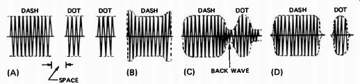
Figure 20. Envelope shapes of dots and dashes that may be radiated
by a code transmitter. The form at (D) is best because it creates the
least interference.
KEYING A TRANSMITTER
When code is transmitted, the carrier is cut on and off in a manner corresponding to the dots and dashes that form coded information. This is called continuous wave (cw) keying. It might at first seem that keying a transmitter would be a simple matter of turning the radiated energy on and off, and that the only signal frequency transmitted would be the carrier frequency. However, the simple act of turning the transmitter off and on by keying it produces sidebands, since this is effectively 100% amplitude modulation using a square wave modulation signal. Thus, if the transmitter is keyed at a rate of 10 times a second, there are two sidebands, one 10 Hz above the carrier frequency and the other 10 Hz below the carrier frequency. A 20 Hz bandwidth would be a very narrow band; however, when a carrier is keyed, it forms a square-top type of signal as shown in Fig.20(A). The harmonic content of such a pulse-like waveform is high. In fact, the amplitude of the second harmonic may be as much as one-half the amplitude of the fundamental frequency. Harmonic components up as high as the 50th can be present in the output signal. As a result, the bandwidth must be wider than the rate of code interruption.
When the transmitter is keyed very sharply, it generates random current and voltage surges, called transients, which produce clicks and thumps in the demodulated sound, and also cause the carrier amplitude to increase at the beginning and end of the dot or dash as shown in Fig.20(B). The very sharp surges of power are also capable of setting up parasitic oscillations, and can cause interference well outside of the assigned channel.
Clicks or thumps heard at the end of each dot or dash can also indicate that the amplifier is not properly neutralized. The amplifier may continue to oscillate and radiate a signal for a short time after the keying has cut off the carrier. This is called a back wave and is shown in Fig.20(C). It can cause the dots and dashes to run together.
Ideal keying occurs as shown in Fig.20(D), when the beginning and end of each individual dot or dash is rounded slightly to prevent harmonics of the keying frequency from being generated. Like wise, the space between the dots and dashes should be completely free of carrier and spurious radiation. This can be done by properly neutralizing the amplifier stage, eliminating all parasitic oscillations, and using a well-regulated power supply.
Keying Methods. Keying in a transmitter can be in the final stage of the transmitter or in one of the low-power stages. If it is in a low-power stage, enough fixed bias is applied to the following stages to keep the plate current cut off or at a low value when there is no excitation to the stage. Although it is possible to key a stage by opening and closing the circuit to any element in the tube, the only practical circuits to key are the cathode or grid circuits. Of the two, the grid circuit is prefer able.
An ideal way to key a powerful cw transmitter is to key the grid of a low-level stage as shown in Fig. 21. When the key is open, the grid bias is increased to a very high negative value, and the plate current is cut off. With the key closed, a normal bias is applied and the stage operates at maximum output. When the key is open, there will be no rf output from the stage. With sufficient bias on the following stages, their plate current will drop to zero when the rf excitation is removed.
Another keying method is shown in Fig.22.
Here the key controls the power relay in the cathode circuit of the stage. The plate current is cut off and on when the relay opens and closes.
This method has the disadvantage that if the stage is handling any appreciable amount of power, the relay contacts must be very large to handle the high current, and the relay must be insulated to take the full plate voltage.
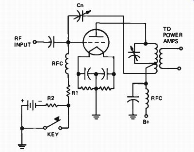
Figure 21. Using key to change bias applied to if amplifier tube.
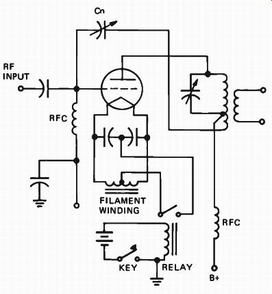
Figure 22. Keying in center-tapped filament circuit.
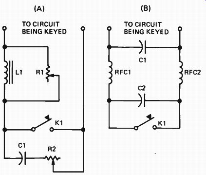
Figure 23. (A) Keying circuit for shaping signal to eliminate thumps; (B) rf filter to remove clicks.
Shaping Dots and Dashes. Proper shaping of dots and dashes is accomplished by means of a keying filter or lag circuit. Figure 23(A) is an example of one type of lag circuit. Choke coil L1 slows the buildup of current in the keyed circuit.
Variable resistance R1, shunting the coil, controls the current through the coil and changes the speed with which the current builds up.
When the key is opened, the magnetic field around the choke coil collapses. The collapsing field causes a current to flow through C1 and R2 that rounds off the trailing edge of the character.
C1 also prevents arcs at the key contacts when the key is opened.
In practice, resistor R1 is adjusted to the lowest value that will prevent thumps when the key is closed. R2 is adjusted to the highest value that will prevent thumps and clicks when the key is opened. The lag circuit is built into the transmitter at the keyed circuit. When a keying relay is used, the lag circuit is connected at the relay contacts.
The leads from the transmitter to the key may pick up some rf. Using a shielded lead between the transmitter and the key, with the shield grounded, will keep this pickup at a minimum, but in some cases there may be considerable pickup even with shielded leads. This rf pickup will cause rf currents to arc across the key contacts when the key is opened, and cause key clicks. The rf filter circuit of Fig.23(B) is connected at the key terminals to prevent rf arcing at the contacts.
Vacuum Tube Keyers. Many of the disadvantages of using a keying relay can be overcome by using a vacuum tube as the relay. One type of vacuum tube keying circuit is shown in Fig.24. A triode tube is connected between the filament center tap of the rf stage and B-. When this triode tube is cut off, no plate current can flow through the amplifier. Removing the bias from the keyer tube by closing the key allows both tubes to conduct.
Bias for the keyer tube is supplied by a separate power supply to resistors R1 and R2.
When the key has been open for some time, capacitor C1 is charged to the level of the bias supply. Closing the key shorts the output of the bias supply through resistor R1 and removes the bias from the tube. However, before the tube can conduct, this charge must drain off C1 through resistor R2. As the charge drains off C1, the tube begins to conduct; the current through the tube increases as its grid approaches zero bias. The action of C1 and R2 shapes the leading edge of the code character.
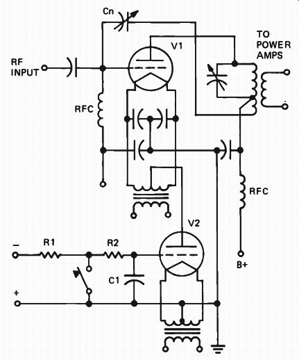
Figure 24. Vacuum tube keying circuit with key-click filter.
When the key is opened, capacitor C1 charges through R1 and R2, and gradually cuts off the current through V2. This shapes the trailing edge of the code character. The entire plate and grid currents for tube V1 must flow through tube V2.
At the same time, the voltage drop across V2 must be kept small. For this reason, V2 is usually two or more parallel-connected tubes which can pass very large currents with small plate-to-cathode voltage drops. Connecting several tubes in parallel increases the current-handling capability of the keyer with out increasing the voltage drop.
SELF-TEST QUESTIONS
17 What is one disadvantage of a grid-modulated class C amplifier?
18 Does the plate power input to a grid modulated class C stage change with modulation?
19 Is 100% modulation possible with screen-grid and suppressor-grid modulation without distortion?
20 Is it necessary to transmit the carrier in an amplitude-modulation system?
21 What is the chief advantage of single-sideband suppressed-carrier modulation?
22 Can a code signal which turns the transmitter on and off 10 times a second be transmitted in a 20 Hz bandwidth?
23 What is the advantage of keying a transmitter in the grid circuit in preference to the cathode circuit?
24 Is it desirable to have the dots and dashes transmitted by a cw transmitter sharp or slightly rounded?
25 What is a vacuum tube keyer?
++++++++++++++++++++++++
Amplitude Demodulation
Earlier in this lesson, you learned that a modulated wave is formed when low-frequency information is superimposed on a higher frequency carrier. The modulated wave then can be trans mitted through space. At the receiver the modulation must be removed from the carrier before it can be used. This process of removing the modulation is called "demodulation." The stage in which demodulation takes place is called a demodulator or a detector.
There have been a number of different types of detectors used for amplitude modulation, but all have disappeared from general use except the diode detector. Both vacuum tube and solid-state diode detectors have been used; the two work in exactly the same way. However, all modern radio and television receivers use either silicon or germanium diodes for amplitude modulation. These detectors are frequently called "linear detectors" because the original modulating signal is produced linearly without distortion.
We are going to confine our discussion of detectors to diode detectors because this is the only type you are likely to encounter.
DIODE DETECTORS
The diode detector is a linear, large-signal detector. This means that the original modulating signal is reproduced linearly without distortion and also that the detector works best on reasonably strong signals. The modulated signal must be amplified by the rf and i-f stages of the receiver until it has a high enough level to operate the diode detector. With the proper signal amplitude fed to the detector input, the output signal is quite linear and reasonably free from distortion. However, when a weak signal is applied to a diode detector, the amount of distortion increases.
Two simple diode detector circuits are shown in Fig.25(A). Notice that the two are identical except in one case where we have shown a vacuum tube diode and in the other case a solid-state diode.
The operation of the two is identical. You may run into a vacuum tube diode detector in an older radio or TV receiver, but you will find solid-state diodes in all modern equipment.
The modulated signal from the rf and i-f amplifier stages is applied between the anode and cathode through the diode load resistor R1 and its filter capacitor C1. The demodulated signal is developed across resistor R1 and capacitor C1. The demodulated signal is fed through the coupling capacitor C2 to the audio amplifier. The operation of these detectors is shown in Fig.25.
When a sine-wave modulated carrier signal, shown in Fig.25(B), is fed to the diode detector, the diode conducts only on the half of each cycle that drives the anode positive.
During the other half-cycle, when the anode is driven negative, the diode does not conduct. As a result, the negative half-cycles are cut off. The output current flows in bursts that occur at the same rate as the carrier frequency. The current flow from the cathode to the anode of the diode is shown in Fig.25(C).
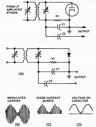
Figure 25. Diode detectors and waveforms.
The peak of each positive alternation causes enough current to flow to charge the output capacitor C1 almost to the peak value of the applied signal. When the applied signal drops below the most positive part of the positive alternation, the diode ceases to conduct. Then the capacitor begins to discharge through the output resistor R1.
However, the time constant of the resistor and capacitor combination is so long that the capacitor discharges only a small amount. By this time, the next alternation of the incoming signal reaches its peak value and draws another burst of diode current that recharges the capacitor.
Therefore, because of the time constant of the RC network, the diode does not conduct for the entire positive alternation of the applied signal, but only during its positive peak. Also, the output voltage no longer follows the carrier variations. It is now a dc voltage that follows the modulation variations, as shown in Fig.25(D). This is the original audio information.
The time constant of the output capacitor and resistor must not be too great or the audio information will also be filtered out. Thus, the time constant of the output circuit must be chosen to act as an effective filter at the carrier frequency, but it must not be long enough to filter the highest frequency component of the modulating information.
The length of time that the diode conducts determines the amount of loading that the diode detector circuit places on the preceding radio frequency amplifier. The less the diode conducts, the lighter the load that the detector places on the preceding stage. Likewise, the efficiency of the detector is higher because the loss in the diode itself occurs only during the interval that the diode conducts. Hence, with a limited conduction time, a greater percentage of the applied modulator energy is developed across the output circuit than is dissipated across the diode.
The ratio of the voltage developed across the output resistor compared to the modulated signal voltage indicates the effectiveness of detector action. The ratio can be made high by making certain that the output resistor has a value much higher than the internal resistance of the diode.
The higher the value of the diode load resistor, the higher the detector efficiency becomes. However, keep in mind that there is a limit to the peak value of the load resistor because of the increase in the output time constant. When very high modulating frequencies are present, such as in high-fidelity and video detectors, the value of the diode load resistor must be kept quite low to prevent loss of the higher modulating frequencies.
Distortion. Diode detectors can introduce frequency, phase, or amplitude distortion into the demodulated signal. Frequency distortion occurs when some of the modulating frequencies are not developed in the output circuit, or do not have the proper amplitude relationship to other frequency components that were present in the original modulating signal. If the output time constant is too long, for example, the high-frequency modulation components may be attenuated with respect to the middle- and low-frequency components.
Phase distortion can also occur in the output circuit and can cause certain modulating frequencies to be delayed with respect to other frequencies contained in the original modulating signal information. Both types of distortion are due to incorrect values of diode load resistor and output capacitor in the diode circuit. They can be reduced by making the detector circuit present a uniformly resistive load to the preceding stage over the band of frequencies contained in the modulation envelope. In addition, the output impedance should be uniform over the entire range of modulating frequencies.
Amplitude distortion occurs when the output voltage does not exactly follow the variations of the modulation envelope. One type of amplitude distortion can be produced when a weak modulated signal is applied to the detector. Notice in Fig.26 that the lower part of the diode characteristic curve is nonlinear. Thus, when a weak signal is applied, the signal is demodulated in this nonlinear portion of the curve. A strong modulated signal, on the other hand, will swing up into the linear part of the curve, and the distortion will be considerably less. Thus, you can see why a high-amplitude signal must be fed to the diode detector for detection with a minimum of amplitude distortion.
Another factor that contributes to amplitude distortion in diode detectors is reverse current flow. In a diode detector using a vacuum tube, this is no problem because when the anode is negative there is no current flow through the tube. How ever, in a diode detector using a germanium or a silicon diode as the detector, there may be an appreciable reverse current. In addition, once this reverse current begins to flow it remains almost constant regardless of the amplitude of the input signal, unless the breakdown voltage of the diode is exceeded. This reverse current tends to discharge the output capacitor on each negative half-cycle.
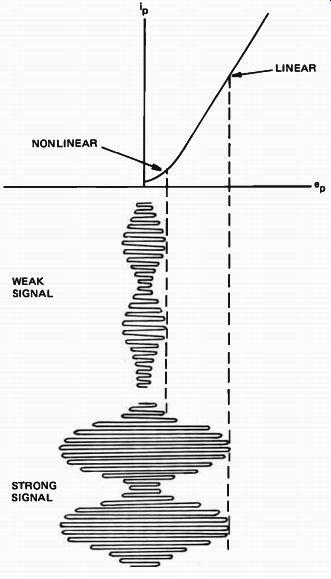
Figure 26. Diode transfer characteristic.
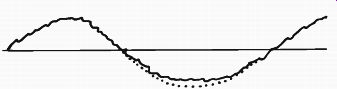
Figure 27. The wavy line shows the distorted waveform; the dotted
line the undistorted waveform.
Since the reverse current remains essentially constant regardless of the amplitude of the signal, this means that you will have a greater percentage of discharging of current on low-amplitude signals than on high-amplitude signals. The reverse current flow of the diode therefore distorts the amplitude of the audio signal and introduces amplitude distortion.
Amplitude distortion can also be produced when the output capacitor is not able to discharge rapidly enough as the modulation envelope falls into its trough. This defect, as shown in Fig.27, actually cuts off a part of the negative alternation of the demodulated signal. The value of the output capacitor should be small enough to present a high reactance to the modulating frequency, and at the same time, its value should be larger than the anode-to-cathode capacity of the diode. A greater part of the applied rf signal voltage will then develop across the diode as it should, and not across the diode output capacitor (which is in effect also shunted across the applied signal). The detector would have low efficiency if a large part of the rf voltage were dropped across the output capacitor.
This type of amplitude distortion is more noticeable on signals having a high percentage of modulation because of the greater voltage change between the crest and trough of the demodulated signal. A greater voltage must be discharged by the output capacitor in order to follow the modulation envelope. For lower percentages of modulation, the amount of voltage that must be discharged between the crest and the trough of the wave is smaller, and the output circuit is able to follow the change.
CW DETECTION
You will remember that when code is trans mitted we referred to the wave as cw (continuous wave). The carrier is modulated by interrupting it to form a series of dots and dashes. When a signal of this type is fed to a diode detector such as shown in Fig.25, the capacitor C1 will be charged, but the amplitude of the charge will be constant.
Thus we would have a dc voltage built up across the capacitor by each dot and dash. Sometimes when a cw signal is fed to this type of detector you can hear a small hiss but you do not have an audible tone. We overcome this in cw detectors by mixing a second signal with the incoming signal.
The second signal is generated by a second oscillator called a beat-frequency oscillator (abbreviated bfo). The beat-frequency oscillator operates at a frequency close to the i-f. Usually a means is provided to vary the frequency of bfo a small amount. The signal from the bfo beats with the incoming i-f signal in the detector and, in effect, amplitude modulates the signal. An audio tone which is equal in frequency to the difference in frequency between the i-f and the frequency of the bfo is produced.
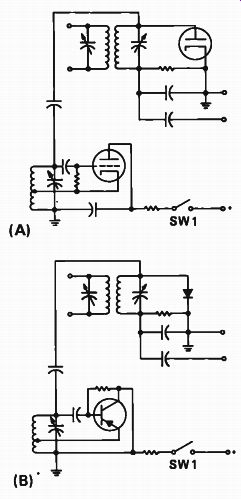
Figure 28. Two detector and bfo circuits.
Figure 28 shows two typical diode detectors along with beat-frequency oscillators. The circuit shown in Fig.28(A) uses vacuum tubes whereas the circuit shown in Fig.28(B) uses a solid-state detector and a transistor as the bfo. The operation of the two is essentially the same. With an incoming i-f of 455 kHz, if the bfo operates at 454 kHz, the two signals will be in phase and add 1000 times each second and they will be out of phase and subtract 1000 times each second. Thus we will have an amplitude-modulated signal that is modulated at a frequency of 1000 Hz. By increasing the frequency of the bfo slightly we can produce a lower frequency audio tone, and by decreasing the frequency we can produce a higher frequency audio tone. The switch SW1 in each circuit provides a means of turning the bfo on for cw reception and off for a standard amplitude modulation reception.
SELF-TEST QUESTIONS
26 Is a diode detector primarily a large-signal or a small-signal detector?
27 What type of diode detector would you expect to find in a modern TV receiver?
28 If too large a diode load resistor is used in the video detector of a television receiver, what is the likely result?
29 How is cw detected with a diode detector?
ANSWERS TO SELF-TEST QUESTIONS
1 Code modulation.
2 Amplitude modulation.
3 1500 watts.
4 50%.
5 30 kHz. You will need 15 kHz to accommodate the upper sideband and another 15 kHz to accommodate the lower sideband. Since these two sidebands are 30 kHz apart, the minimum bandwidth is 30 kHz.
6. 6 watts.
7. Substantially less than 100%. At 100% modulation, the antenna current would be 12.25 amps.
8. Positive carrier shift.
9. It increases four times. The power output increases this much because when the plate voltage doubles, the plate current also doubles so the power output increases four times.
10. 1.4 to 1. The place circuit impedance of the class C stage can be found by dividing the plate current in amps into the plate voltage.
The plate current in amps is 0.125 amp and this when divided into 1000 volts will give you a plate circuit impedance of 8000 ohms.
The turns ratio can then be found by taking the square root of the ratio of the two impedances. You divide 8000 into 16,000 and get 2 and then take the square root of 2 which gives you 1.4 as the turns ratio.
11 These tubes are special zero bias tubes. They are built so that with zero bias very little plate current flows; the tubes are designed especially for class B operation.
12 The plate current does not vary linearly with the plate voltage. In a tetrode or pentode tube, changes in plate voltage have very little effect on the plate current. The plate current is controlled primarily by the screen voltage.
13 Too much power would be wasted in the screen voltage-dropping resistor.
14 It is very inefficient; too much power is lost in the resistors required to reduce the plate voltage of the modulated stage in order to get 100% modulation.
15 The collector current does not vary linearly with the collector voltage.
16 By modulating the collector of the class C amplifier and the collector of the driver driving the class C amplifier.
17 The power output is much lower than can be obtained from a plate-modulated stage.
18 No. The efficiency of this stage and hence the power output changes with modulation.
19 Not in most cases. Close to 100% modulation can be obtained with some special tubes designed specifically for this type of modulation.
20 No. All the intelligence is contained in the sidebands.
21 It produces a narrower bandwidth than a regular AM signal.
22 No. Turning the transmitter on and off produces sidebands far beyond the rate at which the transmitter is turned on and off.
23. Lower powers are handled in the grid circuit than in the cathode circuit and hence it is easier to control clicks and thumps.
24. They should be rounded. This will prevent the clicks and thumps and reduce the bandwidth required to transmit the signal.
25. A vacuum tube keyer is the tube used to key the transmitter. The keyer tube is frequently in the cathode circuit and a high negative bias is placed on the grid when the key opens so the tube is cut off. The transmitter is keyed by removing the grid bias through the keyer tube and hence the class C power amplifier tube can conduct.
26. A large-signal detector. It will produce considerable distortion on small signals.
27. A solid-state diode, either a germanium or a silicon diode.
28. Frequency distortion.
29. By feeding a signal from a bfo into the diode detector along with the i-f signal.
Lesson Questions
Be sure to mark your lesson card as shown to indicate Lesson CC206. Most students want to know their grades as soon as possible, so they mail their lesson card in immediately. Others, knowing they will finish another lesson within a few days, send in two cards at once. Either practice is acceptable. However, don't hold your answers too long; you may lose them. Don't hold answers to more than two sets of lessons at one time, or you will run out of lessons before new ones can reach you.
1. The easiest way to modulate an rf carrier is to use:
a. Morse keying.
b. AM.
c. FM.
d. PM.
2. Amplitude modulation primarily affects which characteristic of an rf signal?
Phase.
Amplitude.
Frequency.
Time.
3. If a 1500 kHz carrier is amplitude modulated by a 2000 Hz sine wave, what frequencies are present at the output of the modulated amplifier?
a. 1300 kHz, 1500 kHz, and 1 700 kHz.
b. 1490 kHz, 1500 kHz, and 1 520 kHz.
c. 500 Hz, 2000 Hz, and 3500 Hz.
d. 1498 kHz, 1500 kHz, and 1 502 kHz.
4. When a sine wave signal amplitude modulates a properly adjusted class C amplifier, what is indicated by the grid and plate current meters?
a. Grid increases; plate decreases.
b. Plate increases; grid decreases.
c. Both remain the same.
d. Both increase.
5. During 100% sinusoidal amplitude modulation, what part of the total average output power is in the sidebands?
a. 100%.
b. 50%.
c. 33-1/3%.
d. 25%.
6. If a transmitter has a modulation index (m) of 1.0, what percent increase in antenna current would you expect?
a. 10%.
b. 22.5%.
c. 33-1/3%.
d. 50%.
7. What is the minimum audio power required to fully plate modulate a class C amplifier that is operating at 3000 volts plate voltage and 400 ma plate current?
a. 600 watts.
b. 750 watts.
c. 900 watts.
d. 1 200 watts.
8. What should the turns ratio be of a modulation transformer to match the class C amplifier of Question 7 to a modulator having an output impedance of 1875 ohms?
a. 0.82.
b. 0.71.
c. 0.50.
d. 0.35.
9. The circuit of Fig.17 uses:
a. Low level modulation.
b. Efficiency modulation.
c. Control grid modulation.
d. All of the above.
10. The purpose of C1 in Fig.25 is to:
a. Match the detector to R1.
b. Couple the audio signal.
c. Bypass the audio signal.
d. Filter the i-f signal.
-------------
THE VALUE OF KNOWLEDGE
Knowledge comes in mighty handy in the practical affairs of everyday life. For instance, it increases the value of your daily work and thereby increases your earning power. It brings you the respect of others. It enables you to understand the complex events of modern life, so you can get along better with other people. Thus, by bringing skill and power and understanding, knowledge gives you one essential requirement for true happiness.
But what knowledge should you look for? The first choice naturally goes to knowledge in the field of your greatest interest--electronics. Become just a little better informed than those you work with, and your success will be assured.
It pays to know--but it pays even more to know how to use what you know.
You must be able to make your knowledge of value to others, to the rest of the world, in order to get cash for knowledge.
This N RI course gives you knowledge, and in addition shows you how to use what you learn. Master thoroughly each part of your course, and you'll soon be getting cash for your knowledge.
------------------
Innovation in learning by a McGraw-Hill Continuing Education School
Based on: NRI Schools (courses)-- A Division of The McGraw Hill Companies Washington, DC 20008, USA.
| Top of Page | Index | PREV | NEXT |