AMAZON multi-meters discounts AMAZON oscilloscope discounts
Table of Contents:
- Introduction
- Semiconductor Types
- N-Type Material
- P-Type Material
- Charges in Semiconductor Materials
- Review
- Self-Test Questions
- Current Flow in Semiconductors
- Diffusion
- Drift
- Review
- Self-Test Questions
- Semiconductor Diodes
- Depletion Layer
- Biased Junctions
- Review
- Self-Test Questions
- How Diodes Are Used
- Silicon Rectifiers
- Zener Diodes
- Tunnel Diodes
- Pin Diodes
- Varactor Diodes
- Point-Contact Diodes
- Light-Emitting Diodes
- Review
- Self-Test Questions
- Answers to Self-Test Questions
- Lesson Questions
-----------------
Lesson Objectives
In this lesson you:
• Learn the principles of semiconductors.
• Explore how current flows in two types of semiconductor material.
• See how semiconductors can be made to form diodes.
• Learn about how different kinds of diodes work.
-----------
INTRODUCTION
Semiconductors are the basic components of transistors. They have been around for a long time, in various forms. Semiconductors were first used in 1905, when a fine-pointed wire pressed against a lead sulphide crystal made a detector for radio receivers. Such "point-contact" diode devices are still available today, but junction diodes are more common and perform better.
We will introduce semiconductors and diodes in this lesson--their construction, operation, and characteristics. A solid understanding of semi conductors and semiconductor junction diodes will help you understand transistor operation.
SEMICONDUCTOR TYPES
A conductor is a material through which electricity can flow readily, and an insulator is a material through which electricity cannot flow. Between conductors and insulators lies another group of materials called semiconductors. Semiconductors are neither good conductors nor good insulators.
Germanium and silicon are semiconductor materials. At one time, germanium was widely used to manufacture diodes and transistors, but today silicon has replaced germanium almost entirely. However, diodes and transistors made of germanium work in the same way as diodes and transistors made of silicon. While we are going to concentrate on silicon, anything we say about the way a silicon diode works applies equally to a germanium diode.
The nucleus of the silicon atom has a charge of +14, and around the nucleus will be 14 electrons, as shown in Fig.1. Notice there are two electrons in the first ring and eight in the second. This is the maximum number of electrons that can be in each of these rings. In the third ring are four electrons called valence electrons, giving the atom a total of 14 electrons to balance the charge of +14 on the nucleus.
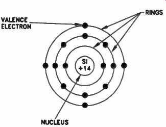
Figure 1. Silicon atom with a charge of +14 balanced by 14 electrons.
The four electrons in the outer ring are called valence electrons.
The outer shells of silicon and germanium are not completely filled with electrons. As a result, the chemical nature of these atoms is to acquire additional electrons. However, one atom cannot pull electrons away from another atom. Instead, nearby atoms will share electrons. Two silicon atoms will share two electrons by bonding, one from each atom, as shown in Fig.2(A) on the next page. By sharing electrons in this way, each atom partly fills its outer shell. This pair of shared electrons is called a covalent bond.
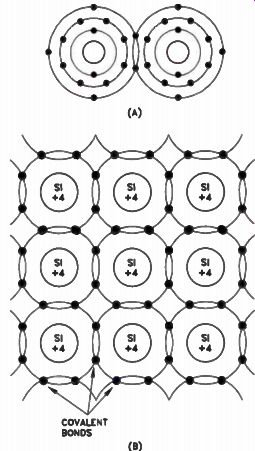
Figure 2. (A) Sharing of two electrons by two silicon atoms and (B)
covalent bonds produced in a silicon crystal.
This bonding process goes further. To fill its outer ring with electrons, a single silicon atom will establish covalent bonds with four other atoms so that each atom's outer ring has 8 electrons. This arrangement of atoms in a piece of silicon is shown in Fig.2(B). Billions of silicon atoms bond into crystal form and arrange themselves into a lattice structure. Each atom shares its four valence electrons with one valence electron from each of its four neighboring atoms to form these covalent bonds.
Even at low temperatures, there is some level of heat energy in all materials. This energy is sufficient to cause a few of the electrons to move out of their proper places in the lattice structure of the silicon crystal and become free electrons.
When an electron moves out of its position in the lattice structure, it leaves an empty space, or hole, in the crystal lattice. An electron from a nearby atom can move into this hole, creating a new hole at the place it left. Another electron may move out of still another atom to fill this new hole, leaving behind it another new hole.
The electrons in a piece of silicon are in a constant state of motion within their atoms. In its movement, if an electron comes closer to a hole than to its own atomic nucleus, it will be strongly attracted to the hole and will leave its atom. When there is no voltage applied across the crystal, this movement of holes and electrons is infrequent and in random directions.
When the movement of an electron out of an atom forms a hole in the atom, the free electron and the hole it forms are called a hole-electron pair. The formation of hole-electron pairs is a continuous process, as is the filling of holes by electrons. As an electron leaves its atom and forms a hole, another electron moves in to fill that hole, leaving a new hole behind it. This action goes on continuously. The random conduction of electricity in pure silicon or germanium caused by the continuous formation of hole electron pairs is called intrinsic conduction.
From an electronics standpoint, this type of conduction is undesirable, and it is much more prevalent in germanium than in silicon. This is one of the reasons silicon has generally replaced germanium in new diodes and transistors.
In its pure form, neither silicon nor germanium is useful in semiconductor devices. Neither material is a good conductor; both are fairly good insulators. But it is possible to alter the characteristics of both germanium and silicon and produce two different types of semiconductor material, both of which are useful in semiconductor devices.
To use silicon and germanium in semiconductors, controlled amounts of other selected elements called impurities are added to the crystals to alter their characteristics. By adding these materials, we can produce two types of silicon and germanium: n-type and p-type.
N-Type Material
An n-type semiconductor material can be made by adding, as an impurity, an element that has five electrons in its outer ring. An example of this type of material is arsenic. Arsenic has a positive charge of 33 on the nucleus and has 33 electrons in the outer shells surrounding the nucleus. Of these electrons, 28 are in the first three rings and 5 are in the fourth ring.
When a small amount of arsenic is added to a silicon crystal, the arsenic atoms form covalent bonds with the silicon atoms, as shown in Fig.3 on the next page. However, only four of the five valence electrons in the outer shell of the arsenic atom can form covalent bonds with the neighboring silicon atoms. Thus, there will be one electron left over after the four covalent bonds are formed. This electron is free to move about within the crystal in exactly the same way a single electron is free to move about the outer shell of an atom in a good conductor. The addition of arsenic, which produces these free electrons, greatly reduces the resistance of the material.
If the silicon has had an impurity added to it, we say it has been doped. When a semiconductor material has been doped with a material such as arsenic, creating an excess of electrons, we call it an n-type material. The "n" refers to the negative carriers, or free electrons. Arsenic is called a donor impurity because it donates an easily freed electron.
In addition to arsenic, other materials can be used as donors. Phosphorous has a total of 15 electrons, and antimony has 51 electrons. Both of these elements have 5 electrons in their outer, or valence, shells, and both have been used in place of arsenic as a donor impurity.
P-Type Material
If we add a material with only three, instead of five, electrons in its valence shell, we have a situation where the impurity added to the semiconductor has one less electron than it needs to establish covalent bonds with four neighboring atoms. Thus, in one of the covalent bonds there will be only one electron instead of two. This will leave a hole in the bond. One material that is frequently used to create these bonds is indium. Indium has 49 electrons arranged around the nucleus in rings of 2, 8, 18, 18, and 3. When indium is added to silicon, it forms covalent bonds with neighboring atoms, as shown in Fig.4.
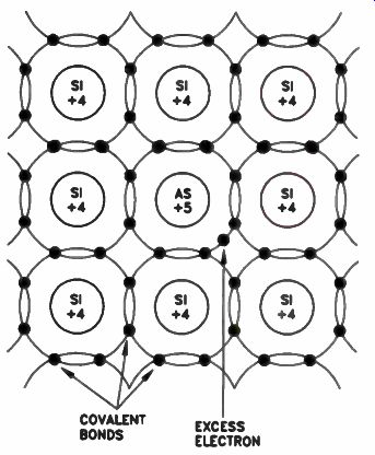
Figure 3. Silicon with arsenic added. Excess electrons are formed.
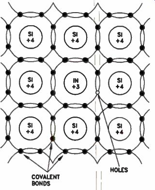
Figure 4. Silicon with indium added. A hole is formed in the covalent
bond between indium and four neighboring silicon atoms because the indium
atom has only three electrons in its outer ring.
The free electrons present in the silicon (as a result of intrinsic activity) are strongly attracted to the holes in the covalent bond that are produced wherever an indium atom has displaced a silicon atom. An electron will move into a hole in the covalent bond, producing a new hole in an other atom and giving the effect that the hole is moving, as shown in Fig.5.
Since a hole in the crystal is caused by an absent electron, a hole has a positive charge.
Therefore, when a semiconductor material has been doped with indium, or with any material that produces holes in the lattice structure, we call the result a p-type material. The "p" stands for positive. Since holes represent the absence of an electron, we say they act as positive carriers.
Indium is called an acceptor impurity because its atoms leave holes in the crystal structure that are free to accept electrons.
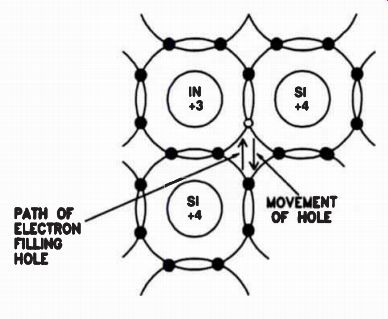
Figure 5. When an electron fills a hole, another hole will seem to move
to where the electron was.
In addition to indium, boron and aluminum can be used as acceptor impurities. Boron has five electrons: two in the first shell and three in the second. Aluminum has 13 electrons: 2 in the first shell, 8 in the second, and 3 in the third.
Charges in Semiconductor
Materials When a donor material is added to silicon, the fifth electron in the valence ring does not become part of a covalent bond. This extra electron is free to move away from the donor atom. When this happens, the donor material, such as arsenic, loses an electron, giving the arsenic atom a positive charge. At the same time, when the free electron moves to a nearby silicon atom, the silicon atom gets an extra electron and a resulting negative charge. The arsenic may then at tract an electron from a nearby silicon atom to neutralize the positive charge, making a hole in that covalent bond and giving the silicon atom that loses the electron a positive charge. This is a continuous process.
The situation is comparable in a p-type material to which indium has been added. Indium has only three electrons in the outer valence ring.
When an electron from a nearby silicon atom moves into the hole in the covalent bond created between the indium atom and its neighboring atoms, there will be one more electron in the indium atom than is needed to neutralize the charge on the nucleus. Thus, there will be a region of negative charge around the indium atom, and there will be a region of positive charge around the silicon atom that has given up an electron.
It is important to realize that although there may be areas of negative or positive charge throughout the crystal, the net charge on the crystal is zero. Even though electrons and holes move within the crystal, the crystal itself has not gained or lost any electrons, because the negative charges and the positive charges balance. The carrier that is present in greater quantity is called the majority carrier, while the other is called the minority carrier. In an n-type material, the electrons are the majority carriers and the holes are the minority carriers. In a p-type material, holes are the majority carriers and electrons are the minority carriers.
Review
In semiconductor materials there is movement of both holes and electrons. They are involved in conduction at all times. Holes are called positive carriers and electrons are called negative carriers. In an n-type material, the electrons are the majority carriers, and in a p-type material, the holes are the majority carriers.
Both n-type and p-type semiconductor materials are used in diodes and transistors. In the next section of the lesson, we will see how current flows through these materials.
Self-Test Questions
1 Which material, silicon or germanium, is more widely used in modern semiconductor devices?
2 How many electrons are there in the outer ring of the silicon atom?
3 How many electrons are there in the outer ring of the germanium atom?
4 Are pure silicon and germanium good electrical conductors?
5 What do we mean when we say that a silicon crystal has been doped? 6 What material is widely used as a donor?
--------------
CURRENT FLOW IN SEMICONDUCTORS
When a p-type material is placed next to an n-type material, they have a junction. The action that occurs at the point of contact between the two different types of material is extremely important.
In this section of the lesson, you will study how current flows through semiconductor materials.
You need to understand current flow through both n-type and p-type semiconductors to be able to understand how a junction works. Once you understand how a junction works, you will study a number of different types of single-junction semi conductors, or diodes. In the following lesson, you will study transistors, which have two junctions.
Diffusion
Adding impurities to pure silicon creates either free electrons or holes. As you learned earlier, there is a certain amount of heat energy present in a crystal, even at relatively low temperatures. This energy produces some motion of free holes or electrons. The motion is random; it has no fixed direction.
When electrons and holes are in motion, they move in opposite directions. Remember that when there is a hole in one atom and an electron moves from another atom to fill that hole, a new hole appears in the second atom. The result is that the effective current flow of any one hole is canceled by the movement of an electron, and the net current flow is zero. That is, if there is a hole in atom 1 and an electron from atom 2 moves over to fill that hole, the hole moves from atom 1 to atom 2. The current flow of the electron is canceled by the movement of the hole.
This random motion of carriers is called diffusion. Diffusion goes on at all times in a crystal, whether or not there is a voltage applied to the crystal. Every effort is made in the design of transistors to keep this diffusion as low as possible, because random carrier motion contributes nothing to useful current flow through the device.
Drift
Another type of carrier movement in semiconductors is known as drift. This type of movement is obtained when a voltage is applied across the crystal. Since the manner in which current flows through n-type and p-type materials is different, let's consider them separately.
N-Type Materials. Figure 6 shows an n-type crystal with a voltage applied to it. The voltage difference supplied by the battery provides a force that makes it easier for the electrons to move in one direction than in the other. The electrons are attracted by the positive terminal of the battery Because the electrons greatly out number the holes, they will carry the current in the n-type material.
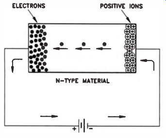
Figure 6. N-type crystal with voltage applied to it.
When an electron moves away from its covalent bond toward the positive battery terminal, it leaves behind an atom with a positive charge, called a positive ion. The electrons moving to ward the positive battery terminal create a region with a local negative charge, as shown in Fig.6. This negative charge establishes a potential difference between that end of the crystal and the positive terminal of the battery. In other words, the attraction of the positive battery terminal causes electrons to bunch up near the end of the crystal connected to the positive terminal and flow into the wire toward the voltage source.
Meanwhile, the atoms left behind are positive ions. A region of positive charge is created at the end of the crystal connected to the negative terminal of the battery. This potential difference pulls electrons from the wire into the crystal.
These electrons replace the free electrons that were attracted to the positive terminal of the battery.
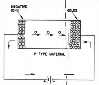
Figure 7. P-type crystal with voltage applied to it.
The number of electrons leaving the crystal through the end connected to the positive battery terminal will be exactly equal to the number of electrons entering the crystal at the end connected to the negative terminal. Since the crystal was electrically neutral before the battery was connected, and since the number of electrons in the crystal remains constant, the crystal itself remains electrically neutral.
P-Type Materials. Conduction through p-type material is quite different from conduction through n-type material. In the p-type semiconductor, nearly all the current is carries the voltage causes the holes to drift toward the negative terminal. They are repelled by the positive battery terminal connected to the one end of the material and attracted by the negative potential applied to the other end. When a hole starts moving away from the end of the material connected to the positive terminal of the battery, it moves because it is filled by an electron attracted from a nearby atom.
When the hole in an acceptor-type (p-type) atom is filled with an electron, the atom has one electron more than it needs to neutralize the charge on the nucleus. Thus the atom has a negative charge; it becomes a negative ion. Negative ions that are formed near the semiconductor end that is connected to the positive terminal build up a region of negative charge at this end of the material. The extra electrons are drawn from these ions by the positive terminal of the battery, and new holes are formed. These holes then drift toward the end of the semiconductor connected to the negative battery terminal and build up a positive charge at this end of the semiconductor. This positive charge attracts free electrons from the external circuit. As a hole is filled with an electron, it disappears.
So, in a p-type material, we have an electron flow in the external circuit from the negative terminal of the battery to the semiconductor and from the semiconductor to the positive terminal.
But in the semiconductor itself, current flows by means of holes, which drift from the end of the semiconductor connected to the positive terminal of the battery to the end connected to the negative terminal. Keep this point in mind: Even in p-type materials (where conduction occurs by holes, or positive carriers), the current flows in the external circuit by electrons (negative carriers) and moves in the conventional direction from the negative terminal toward the positive battery terminal.
It is important to understand that in n-type crystals, the excess electrons (produced when a donor atom forms covalent bonds with four semi conductor atoms) are free electrons that can move about the crystal. But in the p-type material, there are no extra electrons to act as free carriers; the electrons that move can only move to holes. Since a hole can capture an electron from any of its surrounding atoms, it is the hole that is free to move in any direction. For this reason, and because there are more holes than electrons in the lattice, holes are considered to be the majority carriers in p-type material.
The concept of hole-flow is simply a way of representing the action that takes place in the crystal lattice. N-type material has a lot of extra electrons, making electrons the majority carrier by which current flows in the crystal. P-type material has a lot of extra holes, so holes are the majority carrier. Actual circuit current through the p-type material still consists of electrons going in one end of the crystal and coming out at the other end. However, inside the p-type crystal itself, the mechanism of transfer depends upon hole-flow, since the electrons do move by them selves as free electrons but must move from one hole to the next.
An important practical difference between the n-type and the p-type material is that a free electron moves about twice as fast as a hole. This affects the conductivity of the two types of semi conductor material. If we have two crystals, an n-type and a p-type, and the n-type material has the same number of free electrons as the p-type material has holes, the n-type material will have a lower resistance because the free electrons can move approximately twice as fast as the holes in the p-type material.
Review
The important thing to remember from this section of the lesson is that current flow through an n-type semiconductor is a movement of free electrons. They drift from the end of the semi conductor connected to the negative terminal of the battery to the end of the semiconductor connected to the positive terminal of the battery. In the p-type semiconductor, current flows through the crystal by means of holes. They drift from the end of the crystal connected to the positive terminal of the battery to the end of the crystal connected to the negative terminal of the battery.
In both cases, current flow in the external circuit is by means of electrons flowing from the negative terminal of the battery to the crystal and from the crystal to the positive terminal of the battery.
Also, remember that the speed at which electrons move through n-type material is about twice the speed at which holes flow through p-type material. Thus, n-type material has better conductivity and lower resistance than p-type material.
Self-Test Questions
7. In which direction do electrons move through an n-type crystal that has a voltage applied to it?
8. In which direction do holes move through p-type material that has a voltage applied to it?
9. Do electrons move through an n-type material at the same speed as holes through a p-type material?
10. When current is flowing through a crystal, will the crystal be charged?
11. If you had two identical pieces of silicon and one was doped so that it was n-type material, while the other was doped so that it was p-type material, which would have the lower resistance
12. Is diffusion in a semiconductor material desirable?
----------------
SEMICONDUCTOR DIODES
A semiconductor diode is made by taking a single crystal and adding opposite donor impurities to each half, making a single crystal with a p section and an n section. Where the two sections meet, they have a junction. Contacts are fastened to the two ends of the crystal so that it can be connected to an external circuit. Figure 8 shows a simple pn junction. For simplicity we have represented the crystal as a box-like structure with one half p-type material and the other half n-type material.
This type of diode is called a junction diode. At the junction of the p-type crystal and the n-type crystal, the actions of holes and electrons form what is called the depletion layer. Let us see what a depletion layer is and how it is formed.
Depletion Layer
Remember that in an n-type crystal there are free electrons and in a p-type crystal there are free holes. Also remember that the electrons and holes move about a crystal in a random motion called diffusion. In the pn junction diode, holes move about in the p section and electrons move about in the n section. Some of the holes diffuse across the junction from the p section into the n section and are filled by free electrons. Similarly, some of the electrons in the n-type material diffuse across the junction and fill holes in the p section.
When an atom in the n section loses an electron, the atom becomes charged, or ionized. It has a positive charge because it has one less electron than it needs to neutralize the charge on the nucleus. Electrons diffusing across the pn junction from the n side leave behind atoms with a positive charge. At the same time, the atom on the p side gets one more electron than it needs and develops a negative charge.
Similarly, a hole diffusing across the junction from the p side moves into an atom that is, consequently, now missing an electron, giving the atom a positive charge. Over on the p side of the junction, because the hole moved, the atom that gained an extra electron gets a negative charge.
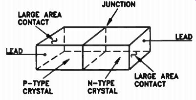
Figure 8. A simple pn junction.
As a result of this diffusion of holes and electrons across the junction, a charged area develops on each side of the junction. On the p side is a negatively charged area, because the atoms have extra electrons. This negative charge, once established, repels free electrons in the n-type material away from the junction.
At the same time, positively charged atoms on the n side repel free holes away from the junction. As a result of these charges, on the p side of the junction there is an area where there are no holes, and on the n side of the junction there is an area where there are no free electrons.
This area around the junction where the majority carriers are missing
is called the depletion layer.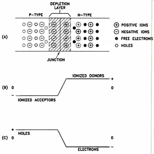
Figure 9. (A) Locations of ions and carriers at a pn junction; (B) charges
at junction due to ionized impurity atoms; and (C) carrier charges.
Figure 9(A) is a drawing showing the concentration of positive and negative ions, as well as free electrons and holes, around a pn junction.
The actual depletion layer of a diode is much narrower than is shown in the picture, where the layer has been enlarged for clarification.
The charge on the ions is shown in Fig.9(B). Notice that on the p side of the junction the atoms that have lost holes by gaining electrons have a negative charge. At the junction, the potential drops to zero and then reverses on the n side where the ionized atoms have a positive charge because they have lost electrons.
Figure 9(C) shows the carrier charges that are available to neutralize the ionized atoms. At some distance from the junction there are holes on the p side with a positive charge. But as we approach the junction, the concentration of these holes decreases because they are repelled from the junction by the positive ions on the n side of the junction. At some distance from the n side of the junction we have free electrons available, but as we approach the junction, the charge drops to zero, because these electrons are repelled from the junction by the negative ions on the p side.
As before, the crystal tends to remain neutral, having no net positive or negative charge. However, there is a region on the p side of the junction where the atoms have a negative charge and a region on the n side of the junction where the atoms have a positive charge. These charges exist only in the area of the junction. The crystal has neither gained nor lost electrons; the overall effect is for the crystal to remain neutral.
Thermal Effects. There is one other important point to consider. Remember that the thermal energy of the crystal keeps the holes and electrons in a continuous state of motion. Even at room temperature, the crystal holds a small amount of heat energy, sufficient to cause motion of both holes and electrons. In the n-type material, an electron leaving an atom creates a hole.
This hole fills with an electron from another atom. There is a continuous formation of hole electron pairs. Away from the junction, this formation of hole-electron pairs does not have any effect on the carrier concentration of the crystal.
Holes produced in the n region near the junction are attracted to the negative ions on the p side of the depletion layer, and some will cross the junction. These holes tend to neutralize the ions on the p side of the junction. Similarly, some free electrons produced on the p side of the junction will cross the junction and neutralize positive ions on the n side of the junction. This is a natural form of intrinsic conduction by minority carriers, due to thermal formation of hole electron pairs.
The effect of minority carriers crossing the junction is to reduce the potential of the barrier created by the depletion layer. When this hap pens, majority carriers are also able to cross the junction at the location of the neutral atoms. The net result is that holes and electrons cross the junction in both directions. These movements tend to cancel each other, but the flow across the junction produces a certain amount of heat, which uses up a percentage of the total capacity of the junction to pass current. This lowered capacity reduces the amount of useful current that the junction can allow to pass. As we mentioned, this type of intrinsic conduction is not desirable, and efforts are made to minimize these effects in semiconductor components.
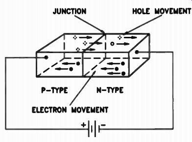
Figure 10. A forward-biased junction.
Biased Junctions
When we connect a battery across a junction diode, we say that the junction is biased. This voltage bias of the diode junction is described as either a forward bias or a reverse bias, depending upon the polarity of the applied voltage. Let's see what we mean by each type of bias and what happens in each case.
Forward Bias. If the positive battery terminal connects to the p-type material, and the negative terminal connects to the n-type material, as shown in Fig.10, we say that the diode is forward-biased.
When the battery is connected with this polarity, a current can flow through the junction.
The positive voltage on the p-type material repels holes toward the junction and attracts electrons from the negative ions in the depletion layer. In the n-type material, the negative terminal of the battery repels electrons toward the junction and pulls holes away from the positively charged ions in the depletion layer. Holes moving toward the junction, and electrons being taken from negatively charged ions, act to neutralize the barrier charge of the depletion layer.
Reducing the potential barrier at the junction allows more majority carriers to cross the junction. More electrons flow from the n-type material across the junction to the p-type material and to the positive terminal of the battery. At the same time, holes travel from the p-type material across the junction toward the n-type material and the negative terminal of the battery.
Normally, we do not connect a battery directly across a diode, because the diode would conduct heavily, overheat, and burn out. Typically, a circuit like the one shown in Fig.11 might be used.
If the diode is a silicon diode, the voltage drop across it will be 0.6 volt. This is the voltage needed to neutralize the depletion layer "barrier charge" at the junction. The remaining 2.4 V is dropped across the resistor. If R had a resistance of 1,000 ohms, the current flow in the circuit would be 2.4 milliamperes. A 500-ohm resistor would allow current of 4.8 mA, with 2.4 V Figure 11. In the series circuit shown, the voltage drop across a silicon diode will be 0.6 volt dropped across the resistor and 0.6 V dropped across the diode.
Remember that the voltage drop in a forward biased silicon diode is 0.6 volt. The actual drop varies slightly (0.6-0.7) according to the temperature, applied voltage, and amount of current through the junction. You will occasionally see references to 0.7 V as the junction potential. A germanium diode, however, drops only 0.3 volt.
The depletion layer is smaller in a germanium diode because there is more intrinsic conduction in germanium.
Notice the schematic symbol for the diode.
(In practice it is often drawn without the circle around it.) The arrowhead is the p-type material and is called the anode. The flat bar is the n-type material and is called the cathode. Since circuit current flows from negative to positive, diode current actually flows against the arrow in the diode symbol. When pioneer studies in the field of electronics were being made, it was not known that electrons had negative charges.
Scientists believed that electrical current flowed from positive to negative. Therefore, the diode symbol was established with the arrow pointing in the direction in which early scientists thought current flowed.
When the two-element vacuum tube, which is called a diode, was invented, scientists soon realized that current was flowing through the tube from the cathode to the anode. This meant that current actually flows from negative to positive.
In order to avoid a lot of confusion, however (since the diode symbol was already established in a lot of published material), the symbol was not changed.
Reverse Bias. Figure 12 shows a reverse bias applied to a junction diode. The negative battery terminal connects to the p-type section and attracts holes away from the junction, in creasing the shortage of holes on the p side of the depletion layer. At the same time, the positive voltage connected to the n-type section of the crystal attracts electrons away from the junction, increasing the shortage of electrons on the n side of the depletion layer. This movement of holes and electrons increases the thickness of the depletion layer and increases the barrier potential across the junction. The increase in the barrier voltage prevents any current flow of majority carriers across the junction.
The current flow across the junction is not zero. A very small minority-carrier current is present through the junction, composed of holes from the n side and electrons from the p side.
Thus, even with a reverse bias, there is a trickle of current flow from the negative terminal of the battery to the p-type material, through the material, across the junction, across the n-type material, and back to the positive side of the battery.
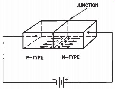
Figure 12. A reverse-biased junction.
This is called a reverse current, in contrast to current in a forward-biased diode, which is called forward current. Normally, we want the minimum possible reverse-current flow, but as you will see later, there are some applications that make use of it.
Review
You should remember that with no voltage applied to a diode, a depletion layer forms at the junction. This depletion layer prevents the further diffusion of majority carriers across the junction. The depletion layer is also sometimes called the depletion barrier, or energy barrier.
When a diode is forward-biased, the negative terminal of the battery is connected to the n-type section and the positive terminal of the battery is connected to the p-type section. With forward bias, current can flow from the negative terminal of the battery to the n-type material, across the material and the junction, across the p-type material, and back to the positive terminal of the battery. We call the current flow in this direction through the diode a forward current flow.
When a diode is reverse-biased, the positive terminal of the battery is connected to the n-type material and the negative terminal is connected to the p-type material. No majority carrier current flows. However, minority carriers still create a very small current through the crystal. This current is called reverse current, and in most cases we want to keep it as low as possible.
Self-Test Questions
13 Which type of ion, positive or negative, will appear in the depletion layer on the p-type side of the junction?
14 Which type of ion, positive or negative, will there be in the depletion layer on the n-type side of the junction?
15 How do you connect a battery to a diode to forward bias it?
16 What is the name given to the current flowing through a diode when it is forward biased?
17 How do you connect a battery to a diode to reverse bias it?
18 What is the name given to current flow through a diode when it is reverse biased?
19 What voltage drop would you expect to find across a forward-biased silicon diode?
----------------
HOW DIODES ARE USED
All semiconductor diodes are composed of some type of pn junction created on a cut or cast segment of crystal. You might think that all diodes work the same, but in fact, there are variations in design that can accomplish a variety of purposes. By varying the amount of doping done to the n-type and p-type materials, and by varying the physical construction of the diode, we can produce diodes with radically different characteristics.
A semiconductor diode is seldom referred to simply as a diode. It usually has a specific name indicating its design type. This section reviews several different types of diodes that you will encounter in your electronics work.
Silicon Rectifiers
A silicon rectifier is a diode made for use as a rectifier in a power supply. It is used in the process of changing AC voltage into de voltage. A typical circuit with a diode used as a rectifier is shown in Fig.13.
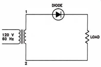
Figure 13. A diode used as a rectifier to convert AC to pulsating dc.
During the half-cycle when terminal 2 is negative and terminal 1 is positive, current flows from terminal 2 of the transformer through the load and the diode to terminal 1 of the transformer. During the next half-cycle, when terminal 2 is positive and terminal 1 is negative, current cannot flow through the diode because the diode is reverse-biased. Therefore, current flows in the circuit for one half-cycle only, in one direction only. This produces a pulsating de out put, since the negative-going half-cycle does not appear across the load.
A silicon diode is an excellent rectifier because it has very low forward-resistance; there is very little voltage drop across the diode when the current is flowing through it. At the same time, the reverse current through a silicon rectifier is very low, so low in most cases that it is not measurable.
This diode has several important characteristics. One is its current-handling capability. Di odes are designed to pass a maximum current in the forward direction. If a diode is used in a circuit where its maximum current rating is exceeded, the junction will overheat and the diode will fail.
Another important characteristic is the peak reverse voltage rating. Looking at Fig.13 again, the diode conducts when terminal 1 is positive and terminal 2 is negative. The voltage drop across it will be about 0.6 volt. But, when terminal 1 is negative and terminal 2 is positive, the entire negative-going voltage of the transformer is applied to the reverse-biased diode. If this voltage exceeds the peak reverse voltage rating, the diode will break down. For instance, if the ratio mean square (rms) voltage from the transformer is 120 V, the peak voltage is 169 volts. You need a diode with a peak reverse voltage rating of at least 200 V to allow a small safety margin.
Silicon rectifiers are made in many different peak reverse voltage (pry) ratings. Low-voltage diodes with a pry of 50 V are typical, as are relatively high-voltage diodes with a pry rating of 1,000 volts. Sometimes you'll see this rating written as piv. This means peak inverse voltage, the same thing as peak reverse voltage.
In the circuit shown in Fig.13, the current that flows through the load is a pulsating current that is present during one half of the AC cycle only. In a later lesson, when you study power supplies, you will learn how this current can be made to flow during both halves of the AC cycle and how it can be changed from a pulsating current to a pure de current.
Zener Diodes
In junction diodes designed for use as rectifiers, we must be careful not to exceed the pry of the diode. Too high a reverse voltage across the junction causes the junction to break down, conduct in the wrong direction, overheat, and fail.
However, zener diodes make use of reverse current. In zener diodes, both the p and the n sections are specially doped and have larger junction areas for increased current-handling capacity. This type of diode is used as a voltage reference and as a voltage regulator. It is also called a voltage-reference diode.
In a zener diode, current remains small at low reverse voltages. At a certain voltage called the breakdown voltage, avalanche voltage, or zener voltage, reverse current increases rapidly with any further increase in reverse voltage.
The breakdown voltage can be varied by modifying the diode construction. Zener diodes can be made with breakdown voltages from 1 V up to several hundred volts. The amount of current that can pass through any zener diode without damaging the diode depends upon the junction area and the methods used to keep the diode cool.
An example of how the zener diode works as a voltage regulator is given in Fig.14. The diode is in parallel with the output and is connected to the unregulated voltage input through a resistor.
To obtain a regulated output voltage of 15 V, we could select a zener diode with a breakdown voltage of 15 volts. The unregulated power supply source would have a voltage of about 20 volts.
The zener diode conducts enough current to maintain the voltage drop across the resistor at 5 V, keeping the voltage drop across itself at 15 V, which is the output voltage. If the unregulated voltage rises to 21 V, the diode conducts more current, increasing the voltage drop across the resistor to 6 V, leaving the regulated output at 15 volts. On the other hand, if the unregulated voltage drops to 19 V, current through the diode decreases so that the voltage drop across the resistor is 4 V, again maintaining the output voltage at 15 volts.
Zener diodes have two important ratings: the breakdown voltage and the wattage rating. The Figure 14. A circuit using a zener diode as a voltage regulator.
wattage rating tells you how much power a zener diode can handle. Most zener diodes are low wattage diodes, with ratings from 1/4 watt up to 1 watt. You can replace a defective 1/4-watt zener diode with a 1-watt zener diode, but if you re place a 1-watt diode with a 1/4-watt zener diode, the low-power device will probably break down.
Tunnel Diodes
A tunnel diode is a junction diode made of germanium or gallium arsenide. Both the n region and the p region of the diode are highly doped. As a result of the high doping, the depletion region around the junction is extremely narrow. Because of the narrow depletion region, holes and electrons can cross the junction by "tunneling" from one atom to another.
Current across the junction increases rapidly with either a forward or a reverse bias. When the bias is zero or very close to zero, current stops.
The current across the junction increases rapidly as the forward bias increases, until a peak is reached. If the forward bias increases beyond this point, the current begins to decrease.
If the forward bias increases still further, the current across the junction continues to decrease, producing a voltage-current curve like the one shown in Fig.15. This decrease in current with increasing voltage results in what is called a negative-resistance characteristic.
Negative resistance is difficult to visualize, but remember from Ohm's law that resistance is equal to voltage divided by current. In a circuit where resistance is constant and applied voltage increases, current also increases.
Similarly, if applied voltage decreases, current decreases. In a tunnel diode there is a region of operation where the opposite happens. If the voltage increases, the current decreases. If the voltage decreases, the current increases. Some thing in the circuit is giving the opposite effect of resistance. We call this negative resistance.
Resistance in the circuit introduces losses. It is the resistance in a resonant circuit that keeps it from continuing to oscillate when power is removed. But if we put something with a negative resistance in the circuit - a tunnel diode, for example - the circuit should continue to oscillate, because negative resistance has the opposite effect of resistance. Tunnel diodes can be used for this purpose; they are also used in switching circuits because they can switch very rapidly. In Fig.15, we've also shown the schematic symbol for the tunnel diode. Compare it to the schematic symbol used for the silicon rectifier and zener diode.
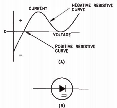
Figure 15. (A) The voltage-current relationship in a tunnel diode and
(B) the schematic symbol for a tunnel diode.
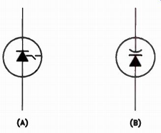
Figure 16. (A) The schematic symbol for a pin diode; (B) the schematic
symbol for a varactor diode.
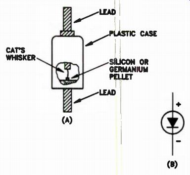
Figure 17. (A) Cutaway view of a point-contact diode and (B) its schematic
symbol.
Pin Diodes
Pin diodes are widely used for high-speed switching in electronic equipment. Pin is an abbreviation of positive-intrinsic-negative. This special diode is doped so that it has a very low resistance with a forward bias across the junction but a very high resistance with a reverse bias across the junction.
Varactor Diodes
Varactor diodes are variable capacitors. In a varactor diode, when the diode is reverse-biased, holes on the p side and electrons on the n side of the junction move away from the junction. The higher the bias, the farther they will move from the junction. This has the same effect as separating the plates of a capacitor, decreasing the capacitance of the junction. Varactor diodes are used as small-value capacitors in specialized circuits, such as electronic tuners, particularly for high-frequency radio.
The symbol used to represent a pin diode is shown in Fig.16(A) and the symbol used to rep resent a varactor diode is shown in Fig.16(B).
Point-Contact Diodes
Another semiconductor used in radio and TV receivers is a point-contact diode, shown in Fig.17 with its schematic symbol. The point contact diode is usually made with a small piece of n-type silicon. The large contact is fastened to one side of the crystal, and a thin wire, called a cat's whisker, is attached to the other side. When a cat's whisker is attached to the crystal, a small region of p-type material is formed around the contact, as shown in Fig.18.
Thus, we have a pn junction. The point-contact diode makes a better detector than a junction diode because the junction between p-type material and n-type material is very small. The diode, therefore, has a lower capacitance and is more sensitive.
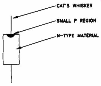
Figure 18. A point-contact diode showing where the p-type material is
formed around the cat's whisker.
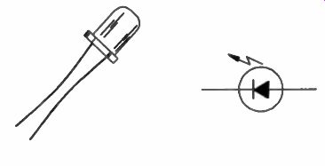
Figure 19. An LED and its schematic symbol.
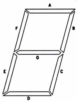
Figure 20. Seven LEDs in a seven-segment array.
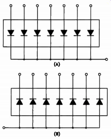
Figure 21. (A) Schematic of a common-cathode seven segment display,
and (B) schematic of a common-anode seven-segment display.
Light-Emitting Diodes
Most pn junctions emit some form of radiation when they are forward-biased. In most cases, however, the radiation is very low and not easily detected. The light-emitting diode (LED) is a diode that has been specifically designed to emit radiation in a particular portion of the spectrum.
A photo of an LED is shown in Fig.19, along with the LED's schematic symbol. In electronic equipment, you will encounter LEDs that emit radiation in the visible spectrum in the form of red, yellow, or green light.
LEDs that emit radiation in the infrared portion of the spectrum are also used in electronic equipment. Many remote-control devices used with TV receivers and VCRs use an LED that emits infrared radiation.
To obtain radiation from an LED, all you need do is place a forward bias across the junction.
This will cause current to flow, producing radiation either in the visible or the infrared part of the spectrum.
Seven LEDs can be arranged as shown in Fig.20 to produce what is called a seven-segment display. Each of these segments is identified by a letter in Fig.20. The LEDs are in a glass or plastic tube so that the light appears as a bar rather than a point of light.
In a seven-segment display, the cathodes of all seven LEDs may be connected, as shown in Fig.21(A) on the next page. When the cathodes are connected, the display is referred to as a common-cathode seven-segment display. The seven-segment display can also be manufactured with all the anodes connected, as shown in Fig.21(B). This type of display is called a common anode seven-segment display.
A seven-segment display can be used to display the numbers from 0 to 9. If all the segments except g are lit, the display will show a 0. If all seven segments are lit, it will display an 8. If segments a, b, g, c, and d are lit, it will display a 3. You can see that by lighting the segments in different combinations, any number from 0 to 9 can be displayed.
Review
We introduced several different diode types in this section. It is important to remember that each of these diodes has an anode and a cathode.
The anode is p-type material, and the cathode is n-type material. Anodes and cathodes are doped n different ways in order to get the desired characteristic from each diode.
You will find all these diodes in electronic equipment; therefore, it is important that you remember both the schematic symbol for each diode and the way in which each diode is used.
In the next lesson, you will study transistors. A transistor is a semiconductor device with two junctions. Many of the electronic devices that we take for granted today were made possible by the invention of the transistor.
Self-Test Questions
20. When we refer to a silicon rectifier, what does peak reverse voltage mean?
21. When a zener diode is used as a voltage regulator, in what direction does the current flow through the diode?
22. What type of diode exhibits a negative resistance characteristic?
23. What type of diode is widely used as a switch?
24. What special characteristic of a point contact diode makes it suitable for use as a detector in radio and TV receivers?
---------
ANSWERS TO SELF-TEST QUESTIONS
1. Germanium was once widely used, but has been replaced by silicon.
2. Four.
3. Four.
4. No. In its pure form, neither silicon nor germanium is a good electrical conductor.
5. When we say that a silicon crystal has been doped, we mean that donor or acceptor atoms have been added to the crystal.
6. A donor material is a material that has five electrons in the outer ring. Arsenic is widely used as a donor.
7. When a voltage is applied to an n-type crystal, electrons move from the end of the crystal that has the negative terminal of the battery connected to it toward the end that has the positive terminal of the battery connected to it.
8. Holes move through a p-type material with voltage applied to it from the end connected to the positive terminal of the battery to the end connected to the negative terminal of the battery.
9. No. Electrons move through an n-type material faster than holes move through a p-type material.
10. When current is flowing through a crystal, the crystal will not be charged, because electrons moving out of the crystal will be replaced by electrons moving into it.
11. The n-type material will have a lower resistance because electrons in an n-type material have a higher mobility than holes in a p-type material.
12. No.
13. Negative ions will appear in the depletion layer on the p-type side of a junction Because holes drifting across the junction to the n side leave behind atoms with a negative charge.
14. Positive ions will appear on the n-type side of the junction because electrons that have left their atoms and diffused across the junction leave atoms with a positive charge.
15. To forward bias a diode, connect the negative terminal of the battery to the n-type material and the positive terminal to the p-type material.
16. Current flowing through a diode when the junction is forward-biased is referred to as the forward current flow.
17. To reverse bias a diode, you connect the positive terminal of the battery to the n-type material and the negative terminal to the p-type material.
18. Current flow through a diode when it is reverse biased is called a reverse current flow.
19. The voltage drop across a forward-biased silicon diode is about 0.6 volt.
20. The peak reverse voltage across the silicon rectifier is the maximum voltage the diode can withstand when the anode is negative and the cathode is positive.
21. Current flows from the anode to the cathode when a zener diode is used as a voltage regulator.
22. The tunnel diode exhibits a negative resistance characteristic.
23. The pin diode is widely used as a switch.
24. The point-contact diode has a very small junction and thus has very low capacitance. This makes it suitable for use as a detector.
-------------
Lesson Summary
Some of the important facts you should remember about this lesson are...
• Silicon can be "doped" with different elements to create a semiconductor material.
• The majority carriers in an n -type semiconductor are electrons, and the majority carriers in a p-type semiconductor are holes.
• At the junction of an n -type material and a p-type material, a depletion layer, or barrier charge, is formed.
• A forward bias across a diode overcomes the barrier charge and allows current to flow from the n -type material to the p-type material.
• A reverse bias across a diode blocks current flow in the direction from the p-type material to the n -type material.
• There are many special types of diodes that have valuable characteristics for specific applications.
LESSON QUESTIONS
This is Lesson Number 2225.
Make sure you print your name, student number, and lesson number in the space provided on the Lesson Answer Form. Be sure to fill in the circles beneath your student number and lesson number.
Reminder: A properly completed Lesson Answer Form allows us to evaluate your answers and speed the results and additional study material to you as soon as possible. Do not hold your Lesson Answer Forms to send several at one time. You may run out of study material if you do not send your answers for evaluation promptly.
1. How many electrons are there in the silicon atom?
a. 8.
b. 4.
c. 14.
d. 32.
2. How many electrons are there in the outer ring of an acceptor-type material, and what type of material will it produce when added to silicon?
a. 3, p-type.
b. 3, n-type.
c. 5, p-type.
d. 5, n-type.
3. How many electrons are there in the outer ring of a donor-type material, and what type of material will it produce when it is added to silicon?
a. 3, p-type.
b. 3, n-type.
c. 5, p-type.
d. 5, n-type.
4. The two layers of ionized atoms at the junction of a pn diode will:
a. Result in an overall charge on the crystal.
b. Prevent minority carriers from crossing the junction.
c. Prevent majority carriers from crossing the junction.
d. Aid majority carriers in crossing the junction.
5. The minority carriers crossing a pn junction will:
a. Have no effect on the depletion layer.
b. Strengthen the depletion layer.
c. Weaken the depletion layer.
d. None of the above.
6. Which of the following diode types is used as a voltage regulator?
a. Zener diode.
b. Tunnel diode.
c. Pin diode.
d. Varactor diode.
7. Which of the following diodes is used as a switch?
a Varactor diode.
b. Point-contact diode.
c. Pin diode.
d. Zener diode.
8. Which of the following diodes has a negative-resistance characteristic?
a. Varactor diode.
b. Tunnel diode.
c. Pin diode.
d. Zener diode.
9. If a 1/2-watt zener diode burns out, which of the following diodes cannot be used as a replacement?
a. A 1/4-watt diode.
b. A 1/2-watt diode.
c. A 1-watt diode.
d. A 2-watt diode.
10. The pry rating tells us the maximum:
a. Allowable voltage across the diode when it is conducting.
b. Allowable voltage across the diode when it is not conducting.
c. Peak current through the diode.
d. None of the above.
---------------------
CASHING IN ON DISCONTENTMENT
Discontentment is a good thing--if it makes you want to do some thing worthwhile. If you had not been discontented with your current situation, you never would have enrolled in your NRI course.
Practically everyone is discontented from time to time. If we allow ourselves to be floored by discontentment, we can easily become complainers who find fault with anything and everything and end up bitter and resentful failures.
If we're smart, we learn to use our discontentment to motivate us. We use it to keep us focused on the goals we have set for ourselves. We know that we are creating a better life for ourselves, so sacrifices are worth making. We are happy in our work. We face defeat squarely and come out winners.
At this moment, you may be discontented with many things - your progress in this course, your current earning ability, or your life in general.
Make that discontentment work for you. Don't let it get you down.
If you do, you may not be able to pick yourself back up again. Keep striving to beat the causes of your discontentment. Remember that it's always darkest before the dawn. And remember, the people who are real successes in life work their hardest when they are face to face with the greatest discouragements and disappointments.
---------------------------