AMAZON multi-meters discounts AMAZON oscilloscope discounts
Table of Contents:
- Introduction
- The Common-Emitter Circuit
- The Common-Emitter NPN Amplifier
- The Common-Emitter PNP Amplifier
- Characteristics of Common-Emitter Circuits
- Review
- Self-Test Questions
- The Common-Base Circuit
- The Common-Base NPN Amplifier
- The Common-Base PNP Amplifier
- Characteristics of Common-Base Circuits
- Review
- Self-Test Questions
- The Common-Collector Circuit
- The Common-Collector NPN Amplifier
- The Common-Collector PNP Amplifier
- Characteristics of Common-Collector Circuits
- Review
- Self-Test Questions
- Field-Effect Transistors
- Junction-Gate Field-Effect Transistors
- Insulated-Gate Field-Effect Transistors
- Dual-Gate MOSFETs
- Review
- Self-Test Questions
- Transistor Characteristics
- Transistor Symbols
- Current Gain
- Review
- Self-Test Questions
- Answers To Self-Test Questions
- Lesson Questions
-------------------
Lesson Objectives
In this lesson you will...
.• Become familiar with the three basic types of transistor amplifiers.
• Learn the differences in NPN and PNP amplifier circuits.
• Discover how amplifier characteristics are matched for input and output circuit impedance.
• Learn how field-effect transistors are used as amplifiers.
• Learn some new symbols and abbreviations for important transistor circuit characteristics.
INTRODUCTION
Many years ago, all electronic equipment used vacuum tubes. There were no transistors. Even giant computers were made of thousands of vacuum tubes. The invention of the transistor led to the development of the integrated circuit (IC). An integrated circuit is simply a device containing many transistors, usually designed to do a certain job.
As manufacturers learned how to stuff more and more transistors into relatively small integrated circuits, more sophisticated devices were developed. The grouping of many transistors into a small package is called large-scale integration (LSI). LSI led to the development of the microprocessor, which is used in industry to control machines, in video cassette recorders to control the operation of the recorder, and in microcomputers. Today's desktop microcomputer can outperform computers that used thousands of vacuum tubes.
Despite the rapid developments in circuit integration, there are many places where discrete (individual and separate) transistors are used.
Learning how transistors operate in these basic "building-block" circuits will help you under stand other circuits that use them.
There are many ways to use a transistor, and one of the most important is to amplify a signal.
A weak signal fed to a transistor amplifier produces a strong signal at the output. Junction transistors and field-effect transistors can both amplify signals. In this lesson we are going to see how transistors are used as amplifiers, beginning with junction transistors.
Junction transistors can be placed into three basic amplifier circuit configurations. These circuits are the common-emitter circuit, the common base circuit, and the common-collector circuit. Of the three, the common-emitter circuit is the most widely used.
THE COMMON-EMITTER CIRCUIT
The common-emitter circuit uses either an NPN or a PNP transistor. Common-emitter amplifier circuits using NPN transistors are a little easier to understand, so we will start the discussion with them.
The Common-Emitter NPN Amplifier
You have learned that a transistor conducts when there is a forward bias across the emitter base junction and a reverse bias across the collector-base junction. In the case of an NPN transistor, this means that the base must be positive with respect to the emitter, and negative with respect to the collector. Another way to state this is that the base must be more positive than the emitter, and the collector must be more positive than the base.
Figure 1(A) shows the battery connections to correctly bias an NPN transistor. Instead of drawing the transistor horizontally, as we did in the previous lesson, we've drawn it vertically. Notice that B1 forward biases the emitter-base-junction and B2 reverse biases the collector-base junction.
Figure 1(B) is the same circuit in schematic form. To forward bias the emitter-base junction, we connect the positive terminal of B1 to the base, and the negative terminal to the emitter.
To reverse bias the collector-base junction, the positive terminal of B2 connects to the collector, and the negative terminal to the base. Figure 1(B) is an exact schematic representation of Fig. 1(A).
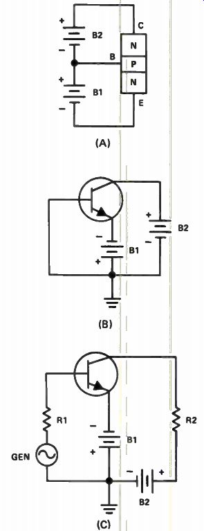
Figure 1. (A) and (B) Correct biasing for an NPN transistor. (C) The
common-emitter circuit.
In Fig.1(C) the circuit is rearranged, but the bias voltages applied to the transistor are un changed. Notice that the positive end of B1 now connects through an AC generator and through R1 to the base. The negative end connects to the emitter, so the emitter-base junction is still for ward biased. The negative terminal ofB2 connects through the generator and R1 to the base of the transistor. The positive terminal connects through R2 to the collector of the transistor. The collector-base junction is still reverse biased.
Notice that we've shown a ground symbol.
This does not change the transistor biasing in any way. We've added this symbol because in the common-emitter circuit, the emitter is normally operated at what is called signal ground potential. In other words, as far as any signal is concerned, the emitter is connected directly to ground. In the circuit shown in Fig.1(C), the battery B1 will have such a low resistance to AC that, for all practical purposes, the emitter is at signal ground potential. If the battery has a high resistance we can bring the emitter to signal ground potential by connecting a large capacitor across the battery. Remember that a large capacitor will have a very low reactance to an AC signal.
The same situation exists in the collector circuit. B2 has a very low resistance, so the lower end of R2 is effectively at signal ground potential. Again, if for any reason B2 had a high resistance, we could bypass it with a large capacitor so that once again the lower end of R2 will be at signal ground potential.
As we said previously, most of the electrons crossing the emitter and the emitter-base junction will cross the base and the base-collector junction and flow through the collector to the positive terminal of B2. B2 will supply the current to the emitter that is eventually going to reach the collector.
Remember also that we said that not all of the electrons crossing the emitter-base junction will cross the base and reach the collector. Some will leave the transistor at the base. B1 will supply these electrons. The current from B1 will flow to the emitter, cross the emitter-base junction, and leave the transistor at the base lead. It will then flow through R1 and the generator back to the positive terminal of B1.
Transistor current supplied by B2 also flows through R2. The current flowing through R2 results in a voltage drop of the polarity shown in Fig.1(C). Normally the value of R2 is selected so that the voltage drop across it will be approximately half the voltage of B2. In other words, if battery B2 has a voltage of 9 volts (V), R2 should drop about 4.5 volts. The voltage drop across R2 subtracts from the B2 supply voltage, so that the voltage between the collector of the transistor and ground is the balance of the supply voltage, about 4.5 volts. Of course, the exact voltage drop across R2 depends on its value and the current flowing through it. The current through the combination of resistor and transistor is also affected by R1 and the voltage applied to the base of the transistor. However, the rule of thumb for common emitter amplifiers is that half the supply voltage is dropped across the collector resistor, R2 in this case.
Thus, with no signal applied (with the AC generator voltage equal to zero), current flows from the negative terminal of B1 across the emitter base junction, through R1 and the generator, and back to the positive terminal of B1. This is a small current, referred to as the input current.
There is also current flow from the negative terminal of B2, through B1 to the emitter, across the emitter-base junction, and out of the transistor at the collector terminal, through R2, to the positive terminal of B2. This current is much larger than the input current, and is called the output current.
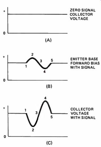
Figure 2. Waveforms for Fig.1(C).
Figure 2(A), on the next page, is a graph representing the collector voltage with zero signal input. That is, in the circuit of Fig.1(C), the generator voltage is 0 volts. The only voltages applied to the transistor are B1 and B2. Under these circumstances, the voltage between the collector of the transistor and ground is constant.
This is represented by the straight, horizontal line. If B2 has a voltage of 9 V, as we mentioned previously, the voltage between the collector and ground will be constant at about 4.5 volts.
Looking again at Fig.1(C), you can see that B1, the generator, and R1 are all connected in series between the emitter and the base. This means that any voltage created by the generator will be in series with the B1 voltage, causing the forward bias across the emitter-base junction to vary.
Figure 2(B) shows what happens to the for ward bias across the emitter-base junction when the generator begins to create a signal. The straight line represents the forward bias supplied by B1. Let's suppose that starting at point 1 in Fig.2(B), the generator voltage adds to the voltage of Bi. Starting at point 1, the signal begins swinging in a positive direction until it reaches a maximum at point 2, then drops to 0 at point 3. At point 3 the polarity of the signal from the generator reverses, and begins subtracting from the voltage of B1. The forward bias then begins decreasing from point 3 to point 4 where it reaches its lowest value. Then, as the generator voltage begins increasing again, so does the forward bias from point 4 to point 5.
When the positive generator voltage adds to the voltage of B1, between points 1 and 3, the emitter current increases because of the increased forward bias. Not only does the current leaving the base and flowing through R1 increase, but the current reaching the collector and flowing through R2 increases. This means that the voltage drop across R2 increases, causing the voltage between the collector and ground to decrease as shown in Fig.2(C). Notice that the relatively larger current flowing through the collector causes the change in voltage between the collector and ground to be much greater than the change in voltage between the base and ground.
When the generator voltage reverses polarity, it subtracts from the voltage applied between the base and emitter by Bi. Thus the net input voltage goes down. This causes the emitter current to decrease so that not only does the current flowing through R1 decrease, but the total current flowing through the transistor and through R2 decreases. When this happens, the voltage drop across R2 decreases so that the voltage between the collector and ground increases, as shown between points 3 and 4 in Fig.2(C). Again, notice that the change in voltage between the collector and ground is much greater than the change in voltage between the base and ground.
There are two very important things to remember: First, the small signal voltage applied to the input (base) of the transistor is reproduced in the form of an amplified or larger signal in the output (collector) circuit. Second, notice that when the input swings positive, the output swings negative. Similarly, when the input signal swings negative, the output signal swings positive. In other words, the input signal has been inverted. The output signal is 180° out of phase with the input signal.
One other important thing to notice about this circuit is that the base current is small and that the generator voltage, when added to the fixed emitter-base forward bias, causes only a small change in base current. That is, the current change in the input circuit is relatively small.
There is a large change in current in the output circuit, however. Since the changing output current is much greater than the changing input current, we say that we have a current gain.
Notice also that the current change in the output is in phase with the current in the input.
To summarize the important points about the common-emitter circuit, we have a voltage gain in the circuit and the amplified voltage is 180° out of phase with the input voltage. We also have a current gain in the circuit and the amplified current appearing in the output circuit is in phase with the input signal current.
A disadvantage of the circuit shown in Fig.1(C) is that it requires two batteries. However, by adding resistor R3, as shown in Fig.3, we can eliminate B1. Current from the negative terminal of B2 flows through R1 and R3 to the positive terminal of B2. The current flowing through R1 develops a voltage across it having the polarity shown. This places a forward bias across the emitter-base junction of the transistor. At the same time, the voltage drop across R3 will be greater than the voltage drop across R2.
Thus, the base is negative with respect to the collector and there is a reverse bias across the collector-base junction.
We've also added capacitors C1 and C2 to the circuit. These capacitors are used to isolate the input and output circuits from the transistor's DC circuits. If the input happened to be a low impedance microphone, without C1 in the circuit, the low-impedance microphone would be in parallel with R1 and upset the forward bias across the emitter-base junction. By putting the capacitor in the circuit, the forward bias will be equal to the voltage drop across R1. The audio signals produced by the microphone are actually AC voltages, which the capacitor will pass.
Bias Stabilization. There is still one problem with the circuit shown in Fig.3. The forward bias across the emitter-base junction of the transistor can change due to minority carriers crossing the collector-base junction. These carriers cause a current flow through R1 in the external circuit that will increase the voltage drop across it. This increases the number of majority carriers crossing the emitter-base junction, which in turn heats the junction. As the junction heats, more minority carriers will cross the junction causing the forward bias on the transistor to increase still further. This action can continue until the transistor gets so hot it literally destroys itself.
This problem can be avoided by adding R4, as shown in Fig.4. Notice that current flowing through R4 develops a voltage so that the emitter is slightly positive with respect to ground. If the minority carriers crossing the emitter-base junction cause the voltage drop across R1 to increase, any increase in majority carrier flow through the transistor increases the voltage drop across R4.
Thus, both the base and the emitter of the transistor become more positive. The increase in positive voltage between the emitter and ground effectively cancels the increase in voltage between the base and ground, and stabilizes the bias. This prevents further increases in non-signal current through the transistor.
Capacitor C3 prevents variations in emitter voltage when a signal is applied to the input.
Without the capacitor, if the input signal causes the emitter current to increase, the voltage drop across R4 will increase. Thus, we have a positive going signal at the base and a positive-going signal at the emitter. The positive-going signal at the emitter tends to cancel or reduce the net change in voltage between the base and emitter.
Similarly, if the input signal swings in a negative direction, the current through the transistor will decrease and this will decrease the voltage drop across R4. Again, this will tend to reduce the net change in voltage between the base and emitter.
This type of signal reduction is called degeneration. In some circuits, degeneration is used to reduce distortion. However, degeneration also reduces the amplification of the stage because it reduces the net change in input voltage applied between the base and the emitter.
With capacitor C3 added to the circuit, the emitter voltage will remain constant when the emitter current changes due to the input signal voltage. C3 is usually an electrolytic capacitor that has a high capacitance, so its reactance is a very small percentage of the resistance of R4.
Another variation of the basic circuit is shown in Fig.5. Notice that we've eliminated the battery and simply indicated the two terminals as + and -. This is common practice in drawing schematic diagrams. The equipment could be battery powered and actually use a battery, or if the equipment is operated from the AC power line, the voltage source would be a DC power supply rather than a battery. As far as the circuit is concerned, it doesn't matter whether the stage is operated from a battery or a power supply; it is going to work in exactly the same way.
Another change we have made is that we've moved R3 so that, instead of connecting it directly to the positive voltage input, we've connected one end of it to the collector. This will introduce some minor degeneration into the circuit, which will reduce distortion.
Remember that when the signal voltage applied to the base swings positive, the current through the transistor increases so the voltage drop across R2 increases. This means that the voltage between the collector and ground swings in a negative direction. This reduces the voltage across the series combination of R1 and R3 so that the voltage at the junction of R1 and R3 will decrease. It will still be positive, but it will go down slightly. Similarly, when the input signal swings in a negative direction, current through the transistor decreases. The voltage drop across R2 will decrease so that the collector voltage will swing in a positive direction. This means that the DC bias voltage at the junction of R1 and R3 will swing in a positive direction.
We can see that, as the amplified signal voltage between the collector and ground swings positive or negative, the voltage at the junction of R1 and R3 will swing in the same way. This voltage change will oppose the input signal voltage and will slightly reduce the stage gain. But it is often worthwhile to accept this slight reduction in the gain of the stage because it reduces distortion so that the amplified output signal is a faithful reproduction of the input signal.
It is important to notice that even though the voltage at the collector of the transistor is about half the voltage at the positive input terminal, we can still maintain a forward bias across the emitter-base junction simply by changing the values of R1 and R3. For that matter, just reducing the value of R3 will reduce the voltage drop across it so that we could maintain the base voltage in the circuit of Fig.5 at exactly the same value as the base voltage in the circuit of Fig.4.
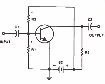
Figure 3. A common-emitter circuit with a single battery.
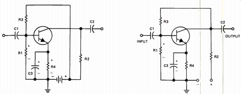
Figure 4. A common-emitter circuit with bias stabilization.
Figure 5. A common-emitter with degeneration.
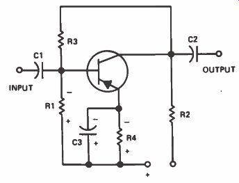
Figure 6. A common-emitter circuit using a PNP transistor.
The Common-Emitter PNP Amplifier
The common-emitter PNP amplifier works in essentially the same way as the NPN amplifier except that the electron current in the external circuit flows in the opposite direction, and the conduction through the transistor is by means of holes.
Figure 6 shows the schematic diagram of a common-emitter amplifier using a PNP transistor. Notice that the polarity of the voltage source is reversed so the positive terminal is grounded and negative voltage goes to the collector through R2. This reverses the polarity of the voltage across R1, so the base is negative with respect to the emitter, a necessary condition to forward bias the emitter-base junction of a PNP transistor. The polarity of the voltage across R4 indicates that electrons are leaving the emitter and flowing through the resistor to ground.
Capacitor C3 is also connected with opposite polarity. R4 serves the same purpose as in the circuit of Fig.5. It stabilizes the forward bias across the emitter-base junction. R3 connects to the collector to introduce degeneration and reduce distortion.
Figure 7 shows waveforms for Fig.6. With zero signal input, the voltage between the collector and ground is negative and constant, and the base voltage is also constant. Figure 7(B) shows an input signal on the base of the transistor.
When the input signal swings in a positive direction as it goes from point 1 to point 2, the negative polarity between the base and ground is reduced. This reduces the number of holes flowing across the emitter, across the emitter-base junction, across the base and base-collector junction to the collector. The number of holes reaching the collector decreases so the electron current flowing through R2 decreases. The voltage drop across R2 decreases, and the voltage between the collector and ground swings in a negative direction, as shown in Fig.7(C). As the input signal drops from point 2 to point 3, the number of holes flowing through the transistor increases. Thus the current through R2 increases as the number of electrons flowing to fill the holes at the collector terminal increases.
The net result is that the negative voltage between the collector and ground decreases as shown between points 2 and 3 of Fig.7(C).
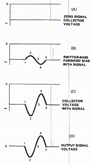
Figure 7. Waveform for Fig.6.
When the input signal swings in a negative direction as it goes from point 3 to point 4 in Fig.7(B), the negative voltage between the base of the transistor and ground increases. This increases the forward bias across the emitter-base junction so the number of holes crossing the junction increases. The number of holes reaching the collector increases, so the number of electrons flowing through R2 to the collector to fill these holes increases. When this happens, the voltage drop across R2 increases and the net voltage between the collector and ground be comes less negative. This is shown between points 3 and 4 of Fig.7(C). Finally, as the input signal voltage swings from point 4 to point 5, the forward bias across the emitter-base junction decreases. This means that current flow in the transistor and through R2 decreases; the voltage drop across it decreases, and the collector voltage swings in a negative direction, as shown between points 4 and 5 in Fig.7(C). If we measure the output voltage at the output end of C2, we see the waveform shown in Fig.7(D). The capacitor, C2, keeps the DC voltage present on the collector from appearing at the output. As the input signal goes through its cycle, it appears in amplified form on the collector, where it is superimposed on the DC collector voltage. However, the capacitor blocks DC voltage at the output, so we have only the amplified AC signal voltage.
Although conduction through the NPN transistor in Fig.5 is by electrons, and conduction through the PNP transistor in Fig.6 is by holes, there are many similarities in the two circuits.
First, in both cases we have a voltage gain, because the amplified output voltage is greater than the input voltage. Secondly, we have a current gain, since the amplified output current flowing in the collector circuit is much larger than the input current flowing in the emitter base circuit. Further, notice that in both cases, the amplified output signal voltage is 180° out of phase with the input signal voltage.
Characteristics of Common-Emitter Circuits
The common-emitter circuit is the most important of all junction transistor circuits because it is by far the most widely used. It is easy to get relatively high gain using the common-emitter circuit. Voltage gains from 80 to 100 are quite easily obtained. This means that the amplified output signal is from 80 to 100 times the amplitude of the input signal.
We mentioned earlier that the collector resistance is selected so that the collector voltage is about half the supply voltage. This allows maximum output signal from the stage. For example, suppose that the supply voltage is 9 V and the collector resistor is selected so that the collector voltage is 4.5 volts. This means that as the current through the transistor varies with the input signal, the collector voltage can swing from 4.5 V to 9 V in one direction and from 4.5 V to 0 V in the other direction, as shown in Fig.8(A) on the next page. Actually, you couldn't go quite that far because the peaks would flatten out and you would introduce distortion, but this is the maximum theoretical swing that you can get in the output voltage.
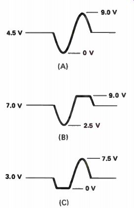
Figure 8. (A) Waveform showing how the output signal can swing from
0 to 9 V with a supply voltage of 9 V and a zero signal collector voltage
of 4.5 volts. (B) and (C) Waveforms showing how the same input signal
will result in distortion if the zero signal collector voltage is too
high or too low.
On the other hand, if the collector voltage were 7 V, then it can only swing to 9 V maximum, for a signal peak of 2 V in the positive direction. A corresponding swing in the negative direction would put the collector voltage at 5 V, leaving 5 V of unused potential. If the transistor is driven harder, there is no additional increase or decrease in collector voltage, so one half of the signal flattens, as shown in Fig.8(B). Similarly, if the collector resistor is chosen so that the voltage on the collector is only 3 V, you would have the situation shown in Fig.8(C). Driving the transistor too hard would result in the other half of the output signal wave being flattened. This flattening of the output signal is one form of distortion.
The changing input signal to the common emitter circuit causes a change in the base current. This, in turn, causes the collector current to change. The changing current is represented by the Greek letter delta, which is written as A. Thus, the changing base current is Aib and the changing collector current is Aie. The ratio of the change in collector current to the change in base current is represented by the Greek letter beta, which is written (3. We can represent this by the formula: 1 3 Aib Since the base current is relatively small, the change in base current produced by the applied signal is small. On the other hand, collector current is much greater than base current, and therefore, the change in collector current is much greater than the change in base current. This means that beta is always greater than 1, and the common-emitter circuit always has a current gain. In other words, the changing current in the output is greater than the changing current in the input.
Two other important characteristics of a transistor amplifier are the input impedance and the output impedance. The input impedance is simply the ratio of the input signal voltage to the input signal current. The signal voltage is the signal applied to the base and the signal current is the part of the base current caused by the signal voltage. If we represent the signal voltage by el, the signal current by Il , and the impedance by Z1 , then the input impedance is: Z1 _ i i
The base current in a transistor is small, therefore the change in base current (the input signal current) is also small. This means that in the common-emitter circuit, the input impedance is relatively high.
Output impedance is the ratio of the output signal voltage to the output signal current. If we represent the output signal voltage by e 2, the output current by i 2, and the impedance by Z2, then the output impedance is:
ei Z 2 _ e2 i2
The output signal current consists of the increases and decreases in collector current produced as the input signal varies the flow of current through the transistor. Even though it is much greater than the change in base current, it also is comparatively small. On the other hand, the change in output current produces a relatively large change in the voltage across the collector load resistor. Therefore, the ratio of the output signal voltage to the output signal current is comparatively high. The common-emitter circuit has a fairly high output impedance--usually about 20,000 ohms.
Review
The common-emitter circuit is the most frequently used junction transistor circuit, and therefore is also the most important. It would be a good idea to read over this section of the lesson again. You should remember that a common emitter circuit provides a voltage gain of about 80-100, and a comparable current gain. Also remember that there is a 180° phase reversal in the signal voltage. This means that the output signal is 180° out of phase with the input signal.
You will see later that there are other junction transistor circuits where this phase reversal does not occur.
Self-Test Questions
1 Is it possible to get a current gain using the common-emitter circuit?
2 What is the relationship between the input signal voltage and the amplified output signal voltage in the common-emitter circuit?
3 Draw schematic diagrams of common-emitter circuits using NPN and PNP transistors. You should try to do this from memory since it is important to remember these circuit con figurations.
----------------
THE COMMON-BASE CIRCUIT
In a common-emitter circuit, the input signal is applied between the base and ground. The output signal is taken from between the collector and ground. The emitter is operated at signal ground potential and is common to both the input and output circuits. In the common-base circuit, the input signal is applied between the emitter and ground and the output signal is taken from between the collector and ground.
The base is operated at signal ground potential, and therefore, is common to both the input and output circuits.
NPN and PNP transistors can be used in the common-base circuit. The circuit using the NPN transistor is a little easier to understand, so we will study it first.
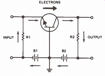
Figure 9. An NPN transistor in a common-base circuit.
The Common-Base NPN Amplifier
Figure 10. An NPN common-base amplifier using a single voltage source.
Figure 9 is a schematic diagram of a basic common-base NPN amplifier. B1 supplies the for ward bias for the emitter-base junction. The negative terminal of B1 connects to the emitter through R 1 . The positive battery terminal and the transistor base are both grounded and there fore connected. In this configuration, the emitter is negative with respect to ground. Since the base is grounded, it is positive with respect to the emitter, which is the condition we need in order to forward bias an NPN transistor.
B2 supplies the reverse bias across the collector base junction. Notice that the negative terminal of B2 is grounded and the positive terminal connects to the collector through R2. This makes the collector positive with respect to the base, reverse biasing the collector-base junction.
With no signal applied, there is a small current through the base, coming from Bi. Electrons leaving the battery flow through R1, the emitter, and the emitter-base junction. They leave the transistor by the base lead and flow back to the positive terminal of Bi.
B2 supplies the collector current. Electrons leaving the negative terminal of B2 flow through B1 and R1 to the emitter of the transistor. They cross the emitter, the emitter-base junction, the base, the base-collector junction, and the collector.
They exit through the collector terminal, then flow through R2 back to the positive terminal of B2.
The circuit shown in Fig.9 is functional, but has several disadvantages. Neither the input nor the output is isolated from the transistor.
Another drawback is that the circuit requires two batteries. The modified circuit in Fig.10 eliminates these disadvantages.
Although it looks very different, Fig.10 shows a common-base amplifier, and works like the circuit in Fig.9. There is one voltage source, which could be a battery or other de source.
Forward bias for the emitter-base junction is created by a voltage divider composed of the resistors R3 and R4. The resistor values are selected to make the base more positive than the emitter. Capacitor C2 keeps the base at signal ground potential by having a reactance that is practically zero at the operating frequency.
Capacitor C1 isolates the input signal from the emitter circuit and C3 isolates the collector from the output signal.
In operation, current flows from the voltage source through R1 to the emitter, creating a voltage drop across R1 that makes the emitter positive with respect to ground. Resistors R3 and R4 form a voltage divider that maintains for ward bias by keeping the base more positive than the emitter. Thus, if the voltage drop across R1 is 1 V, making the emitter voltage equal to +1 V, values of R3 and R4 are selected to set the base voltage to +2 volts.
A few electrons (less than 5%) crossing the emitter and the emitter-base junction exit at the base and flow through R4 back to the voltage source. Most electrons cross the base, the base collector junction, the collector, exit the transistor at the collector terminal, and then flow through R2 back to the voltage source. As in the case of the common-emitter circuit, the value of R2 is selected so that the collector voltage with zero signal is approximately one half the supply voltage.
With zero signal input, the collector voltage is constant as shown in the waveform of Fig.11(A). The emitter and base voltages are also constant.
The emitter voltage is positive; the base voltage is positive and greater than the emitter voltage in order to forward bias the emitter-base junction. The waveform of Fig.11(B) shows what happens to the emitter voltage with a single cycle of an input signal. With the first half-cycle, when the input signal is positive, the voltage increases from the zero signal value at point 1 up to point 2 where it reaches peak positive value. Notice that the signal voltage adds to the emitter voltage.
During the next quarter-cycle, the signal voltage decreases, causing the emitter voltage to fall from point 2 to point 3. In the second half-cycle, the input signal reverses polarity and subtracts from the emitter voltage. Emitter voltage decreases until the signal voltage reaches its peak, negative value at point 4. In the last quarter-cycle the signal voltage moves back toward zero, causing the emitter voltage to increase to point 5, where once again it is at the zero signal level.
As the emitter voltage changes with the changing signal voltage, the base voltage remains constant. C2 is too large a capacitor to either charge or discharge as the signal goes through its cycle. This means that as the emitter voltage increases above the zero signal value during the positive half-cycle of the input signal, the emitter-base forward bias decreases during this part of the cycle. For example, suppose the emitter voltage is +1 V and the base voltage is +2 volts. The difference in voltage between the two is 1V, with the base being +1 V positive with respect to the emitter. If the input signal during the positive half-cycle increases the emitter voltage from 1V to 1.5 V, then the difference of potential between the base and emitter will drop from 1 V to 0.5 V, reducing the forward bias across the emitter-base junction. This is shown in the first half-cycle of the waveform of Fig.11( C ). In contrast, during the next half-cycle, as the emitter voltage decreases, forward bias of the emitter-base junction increases. If the emitter voltage emitter goes from 1 V to 0.5 V during the negative half-cycle, forward bias of the emitter-base junction increases from 1 V to 1.5 volts. This is shown in the second half-cycle of the waveform in Fig.11(C). When the forward bias decreases, as it does during the first half-cycle of the input signal, current through the transistor decreases. Collector current decreases, and so does the voltage drop across R2. When the voltage drop across R2 decreases, the voltage measured between the collector and ground increases as shown in the first half-cycle of the waveform in Fig.11(D). During the next half-cycle, when forward bias increases, current through the transistor increases. This raises the voltage drop across R2.
The voltage measured between the collector of the transistor and ground goes down as shown between points 3, 4, and 5 of the waveform in Fig.11(D).
Figure 11. Waveforms for circuit shown in Fig.1.
With an input signal there exists an output signal like the one shown in Fig.11(E). Compare the output signal with the input signal. Notice that the output signal is larger, so there is voltage amplification. Also notice that it swings positive when the input signal swings positive. There is no phase reversal between the input and out put signals as is the case for a common-emitter circuit. In common-base circuits, the amplified output signal is in phase with the input signal.
Notice that the input current is the emitter current, not the base current. All current in a transistor flows through the emitter. Some emitter current will split off at the base, making the collector current slightly less than the emitter current. You don't see the great differential in input current versus output current that is present in common-emitter amplifiers, where tiny variations in base voltage and current cause large variations in the emitter and the collector current. There is no current gain in a common base amplifier. The collector (output) current will always be less than the emitter current.
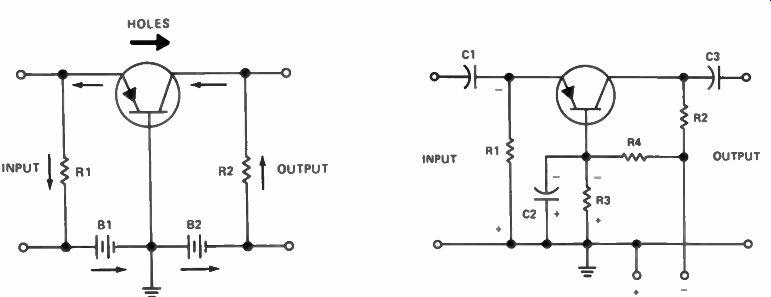
Figure 12. A PNP transistor in a common-base circuit.
Figure 13. A PNP common-base amplifier using a single voltage source.
The Common-Base PNP Amplifier
Figure 12 shows a common-base amplifier using a PNP transistor. Compared to Fig.9, the battery polarities are reversed, and current flow in the external circuit is in the opposite direction.
Conduction through the transistor is from the emitter, through the base, and to the collector by means of holes.
B I provides forward bias for the emitter-base junction. As connected, the base is negative with respect to the emitter. This condition is required to forward bias the emitter-base junction of a PNP transistor. On the other hand, the collector is connected to be negative with respect to the base, which places the necessary reverse bias on the collector-base junction of a PNP transistor.
B1 supplies the base current. Electrons leave the negative terminal of B1 and enter the base where they fill holes. An electron leaving the emitter of the transistor will create a hole. The electron will flow through R1 and back to the positive terminal of B1.
B2 supplies the collector current. Electrons leaving the negative terminal of B2 flow through R2 to the collector where they fill holes arriving at the collector. Electrons are pulled out of the emitter by the positive potential of B2, creating holes. The holes flow across the emitter, the emitter-base junction, the base, and the base collector junction. They finally flow to the collector terminal where they are filled by the electrons coming from the negative terminal of B2. The electrons leaving the emitter will flow through R1 and B1 to the positive terminal of B2.
In Fig.13, we modified the basic circuit to eliminate the two batteries, and to add capacitors for isolating the input and output. Notice that the positive terminal of the voltage source is grounded. The negative terminal connects to the collector through R2. The negative terminal also connects through R4 and R3 to ground. As a result, there is a current flow from the negative terminal through R4 and R3 to ground. Current flowing through R3 produces a voltage drop so that the base is negative. Electrons leaving the emitter of the transistor flow through R1 to reach the positive voltage source. This sets up a voltage drop across R1 so that the emitter is negative with respect to ground.
However, by selecting the correct values for R3 and R4, we can make the voltage on the base greater than the voltage on the emitter, which makes the base negative with respect to the emitter.
The waveforms in Fig.14 show what happens when a signal is applied to the input. With no signal, the collector voltage is negative and constant, as shown in Fig.14(A), as are the emitter and base voltages. The base is more negative than the emitter; that is, if the emitter voltage is -1 V, the base voltage might be -2 volts.
Figure 14(B) shows what happens to the emitter voltage when a signal is applied. The emitter voltage is at its zero signal level at point 1.
During the first half-cycle, as the input signal swings positive from point 1 to point 2 and back to point 3, the input signal drives the emitter voltage in a positive direction. The emitter voltage might drop from -1 volt to -0.5 volt. Now the forward bias across the emitter-base junction is -1.5 V instead of being 1 V as it was with zero signal input. The forward bias across emitter base junction increases as shown in Fig.14(C). The increase in forward bias causes the number of holes flowing through the transistor to increase. When this happens, additional electrons flow from the negative terminal of the voltage source, through R2, to the collector. The voltage drop across R2 increases so that the voltage between the collector of the transistor and ground decreases as shown between points 1, 2, and 3 of Fig.14(D).
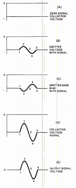
Figure 14. Waveforms for circuit shown in Fig.13.
When the input signal swings in a negative direction, as it does between points 3, 4, and 5 of Fig.15(B), the forward bias across the emitter base junction decreases as shown in Fig.14(C). This causes the number of holes flowing through the transistor to decrease, so the number of electrons flowing through R2 to fill these holes also decreases. The voltage drop across R2 decreases so the potential between the collector and ground increases as shown in Fig.14(D). The output signal with the DC collector voltage removed is shown in Fig.14(E). Notice that once again we have a voltage gain.
Also, the output voltage is in phase with the input voltage. Furthermore, as in the NPN version of the common-base circuit, current in the input circuit flowing through R1 is greater than the current in the output circuit flowing through R2. Thus, there is no current gain in the PNP amplifier either.
Characteristics of Common-Base Circuits
Even though the action of the PNP transistor is quite different from the action of the NPN transistor, the net result using the common-base circuit is the same with both types of transistors.
In both cases, we have voltage amplification and the output voltage is in phase with the input voltage.
Because some of the emitter current flows to the base in the common-base circuit, the collector current must be less than the emitter current. Similarly, any change in the emitter current produced by the applied signal results in some of the changing current flowing to the base and the remainder to the collector. Therefore, the change in current in the collector circuit is less than the change in current in the emitter circuit.
The ratio of the change in the collector current to the change in the emitter current is represented by the Greek letter alpha which is written as ‘a’. We write this in the formula:

Since the change in collector current is always less than the emitter current, alpha always has a value of less than 1. This means that for a given signal, the change in collector current is less than the change in emitter current. We say the circuit has a current gain of less than 1, which means that the changing output current is less than the changing input current. In a good transistor, alpha is 0.99 or greater.
We mentioned that the common-emitter amplifier had a relatively high input impedance.
If we examine the common-base circuit shown in Fig.10 and Fig.12, we see that the input voltage is applied across R1. This causes some signal current to flow through the resistor R1. In addition, the entire emitter current drawn by the transistor must flow through R1. Therefore, even with the small signal voltage, the signal current must be quite high. Since the input impedance is determined by the ratio of the signal voltage to the signal current, a high current causes the ratio of the voltage divided by the current to be low. In other words, the common base circuit has a relatively low input impedance.
On the other hand, since the stage is capable of giving voltage gain, the output voltage which is developed across R2 is much higher than the input voltage. And since the collector current is less than the emitter current, the signal current flowing in the output is lower than the signal current flowing in the input. Thus, the output impedance is higher than the input impedance.
In fact, the output impedance is quite high.
Therefore, in the common-base circuit, we have a very low input impedance and a reasonably high output impedance.
Review
The common-base circuit has a current gain of less than 1. The stage is capable of providing voltage amplification, and the amplified output signal is in phase with the input signal. The common-base circuit has a low input impedance and a reasonably high output impedance, so it is often used in applications where we want to match a low impedance to a high impedance. It is also used in some very high-frequency applications.
Self-Test Questions
4 In a common-base circuit, is it possible to get a current gain?
5 What is the phase relationship between the amplified signal voltage and the input signal voltage in a common-base circuit?
6 Why is it possible to get a voltage gain in a common-base amplifier even though there is no current gain?
7 What are the relative input and output impedances of the common-base amplifier circuit?
----------------------
THE COMMON-COLLECTOR CIRCUIT
The third possible circuit configuration using a junction transistor is the common-collector circuit, frequently called an "emitter follower." In this type of circuit, the collector is operated at signal ground potential. Although this circuit is not found as often as the common-emitter circuit, it does have some characteristics that are useful in certain applications.
As with the previous circuit configurations, either an NPN or a PNP transistor can be used in the common-collector circuit. In this circuit, the input signal is applied between the base and ground and the output signal is taken from between the emitter and ground. Since the collector is operated at signal ground potential, it is common to both the input and output circuits.
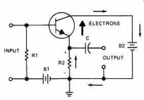
Figure 15. Basic common-collector circuit using an NPN transistor.
The Common-Collector NPN Amplifier
Figure 15 shows the basic common-collector circuit using an NPN transistor. Battery B1 has a low impedance as far as the signal is concerned,
so the signal is effectively applied between the base of the transistor and ground. Capacitor C, connected to the emitter, has a low impedance at the signal frequency, so the output signal is taken with respect to the emitter and ground.
B1 supplies forward bias across the emitter base junction. Current flowing through R2 develops a voltage which subtracts from the bias between the base and emitter, but the voltage drop across R2 is never greater than the voltage of B1 If it were, the transistor would have no forward bias of the emitter-base junction and no current flow through the transistor. If current stops flowing in the transistor, current also stops through R2 and there would then be no voltage drop across it.
Battery B2 supplies the reverse bias across the collector-base junction. The negative terminal of this battery is connected through B1 and R1 to the base of the transistor and the positive terminal is connected directly to the collector. The voltage of B2 is much higher than the voltage at B1 so that as far as the collector base junction is concerned, it is reversed biased.
The arrows on the diagram indicate the main direction of current flow. Electrons leaving the negative terminal of B2 flow through R2 to the emitter. They cross the emitter, the emitter-base junction, the base, the base-collector junction, the collector, and flow back to the positive terminal of B2. A few electrons leave the negative terminal of B1 and flow through R2 in the direction shown. They cross the emitter-base junction, leave the transistor by the base lead and flow through R1 back to the positive terminal of B1.
The disadvantages of the circuit shown in Fig.15 are that it requires two batteries and the input is not isolated from the base of the transistor. We've added the capacitor C1 in Fig.16, on the next page, to isolate the input from the base circuit and also have added R3 to eliminate the need for a second voltage source. We've also simply indicated the + and - terminals where the voltage source is connected. This could be a battery or a de power supply operated from the AC power line.
In this circuit, electrons from the negative terminal of the voltage source flow through R1, developing a voltage drop across it with the polarity shown. The electrons flow on through R3 and back to the positive terminal of the voltage source. Electrons also leave the negative terminal of the voltage source and flow through R2 to the emitter of the transistor, through the transistor, and back to the positive terminal of the voltage source. Once again, even though the emitter of the transistor is positive with respect to ground (due to the current flowing through R2), the values of R1 and R3 are selected so the base is more positive than the emitter and the transistor emitter-base junction is forward biased.
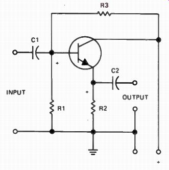
Figure 16. Common-collector amplifier using an NPN transistor and a single
voltage source.
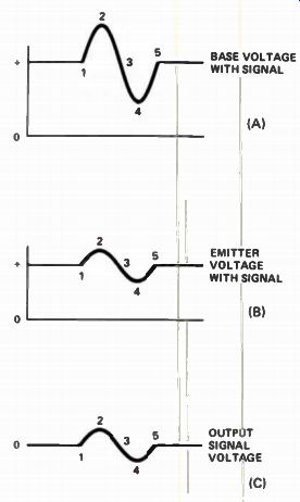
Figure 17. Waveforms for circuit shown in Fig.16.
With zero input signal, the base and emitter voltages are constant. This is represented in Fig.17 by the straight, horizontal line up to point 1 in Figs.17(A) and (B). When a signal is applied between the base and ground during the positive half-cycle, the base voltage starting at point 1 increases to point 2, then returns to zero signal level at point 3. The increase in forward bias across the emitter-base junction causes the emitter current to increase so that the emitter voltage swings from point 1 to point 2 and then back to point 3 as shown in Fig. 17(B).
During the negative half-cycle, as the base voltage swings in a negative direction from point 3 to point 4 and then back to point 5, as shown in Fig.17(A), the emitter voltage also swings in a negative direction. This is because the current through the transistor decreases due to the decreased forward bias across the emitter-base junction. As a result, the current through R2 decreases so that the voltage between the emitter of the transistor and ground goes from point 3 to point 4 and then back to point 5 as shown in Fig. 17(B). Notice that when the base voltage swings in the positive direction, the emitter voltage also swings in a positive direction. This swing in the positive direction reduces the net change in forward bias across the emitter-base junction.
Similarly, during the negative half-cycle, when the base is swinging in a negative direction, the emitter also swings in a negative direction, which once again reduces the net change in emitter-base junction bias. This is degeneration.
Because the emitter signal is subtracting from the base signal, it can never exceed the amplitude of the base signal. If it were to exceed the amplitude it would completely cancel the change in the base voltage. If this happened, there wouldn't be any change in emitter voltage.
The output signal voltage taken between the output terminals is shown in Fig.17(C). Notice that this voltage is zero with zero signal input and then follows the emitter voltage as the signal goes through its cycle. This happens because the reactance of C2 is so low at the signal frequency that, as far as the signal is concerned, it is simply not there. However, C2 does block the de voltage at the emitter of the transistor and prevents the output from shorting out R2.
From the waveforms in Fig.17 we see that the output voltage is originally less than the input voltage. We say that the common-collector circuit has a voltage gain of less than 1. We also see that the output voltage is in phase with the input voltage. The input signal current is the change in the base current, which is relatively small, and the output signal current is the change in the emitter current, which is relatively large; therefore, the common-collector circuit has a current gain.
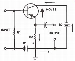
Figure 18. Basic common-collector circuit using a PNP transistor.
The Common-Collector PNP Amplifier
In the common-collector PNP amplifier shown in Fig.18, we have essentially the same circuit as in the case of the NPN amplifier, except that the battery connections are reversed and conduction through the transistor is by means of holes instead of electrons.
Since the current through the external circuit flows the opposite of the NPN circuit, the voltage drop across R2 has the opposite polarity. In other words, the end connected to the emitter is negative and the grounded end is positive.
The negative terminal of B1 connects through R1 to the base of the transistor, and the positive terminal connects through R2 to the emitter.
This battery makes the base negative with respect to the emitter, creating the condition needed to forward bias the emitter-base junction of a PNP transistor. The positive terminal of B2 connects through B1 and R1 to the base of the transistor, and the negative terminal connects to the collector. This makes the collector negative with respect to the base, reverse biasing the collector-base junction.
During operation, electrons leave the emitter through R2 to get to the positive terminal of B2.
This produces holes that cross the emitter, the emitter-base junction, the base, the base-collector junction, and the collector, where they are filled by electrons from the negative terminal of B2. At the same time, the positive terminal of B1 pulls a few electrons from the emitter. The holes produced cross the emitter and the emitter-base junction where they are filled by electrons coming from the negative terminal of B1, through R1, and to the base.
Figure 19 shows the circuit modified to eliminate the second battery. In this circuit, electrons leave the negative terminal of the voltage source and flow through R3 and then through R1 back to the positive terminal of the voltage source. The electrons flowing through R1 create a voltage drop across this resistor having the polarity shown. This drop makes the base negative with respect to ground. Electrons leave the emitter of the transistor to produce holes and flow through R2 to the positive terminal of the voltage source and set up a voltage drop across R2 having the polarity shown. This means that the emitter is negative with respect to ground.
However, the voltage drop across R1 is greater than the voltage drop across R2, so the base is negative with respect to the emitter.
Waveforms for the circuit in Fig.19 are shown in Fig.20. As with the previous circuit using the NPN transistor, both the base and emitter voltages are constant with zero signal. But during the positive half-cycle of an input signal, the base voltage decreases as shown, from point 1 to point 2 and then back to zero signal-voltage level at point 3 in Fig.20(A). The decrease in the base voltage reduces the forward bias across the emitter-base junction, causing the number of holes flowing through the transistor to decrease.
This means there are fewer electrons coming out of the emitter terminal and flowing through R2.
The voltage drop across R2 decreases from point 1 to point 2 and back to point 3, as shown in Fig.20(B).
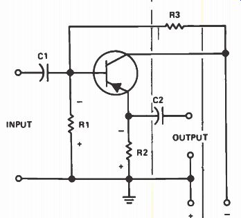
Figure 19. Common-collector amplifier using a PNP transistor and a single
voltage source.
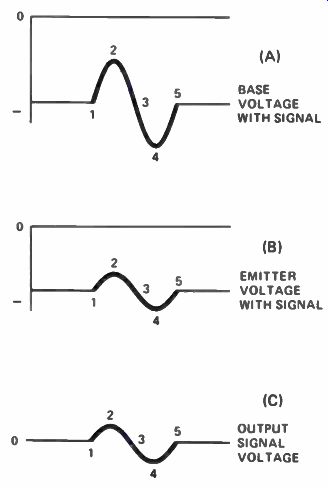
Figure 20. Waveforms for circuit shown In Fig.19.
During the next half-cycle, when the input signal swings in a negative direction, as shown from point 3 to point 4 and back to point 5 in Fig.20(A), the base is made more negative. This increases the forward bias across the emitter base junction so the number of holes flowing through the transistor increases. Thus, additional electrons are pulled from the emitter to create these holes, and the voltage drop across R2 increases, as shown between points 3, 4, and 5 of Fig. 20(B). The output signal is shown in Fig.20(C). Once again, notice that the signal is the same as the signal at the emitter. The output voltage is less than the input voltage, but is in phase. Since change in the base current due to the input signal is relatively small, and changes in the emitter current are large, there is a current gain.
Therefore, the common-collector circuit using a PNP transistor has essentially the same characteristics as those for the NPN transistor.
Characteristics of Common-Collector Circuits
The common-collector circuit has the highest input impedance of the three circuits. Refer to Fig.15. Input impedance is the ratio of the input voltage over the input current. The voltage applied at the input causes a flow of signal current from the emitter, through the transistor, and to the collector. Some electrons traveling from the emitter to the collector exit through the base and R1. But, since the output signal voltage is sub tracted from the input signal voltage, as far as the signal voltage applied between the base and emitter is concerned, the actual signal current in the transistor is quite small. Therefore, the total input signal current is small, and this means the input impedance is high.
On the other hand, the output impedance of the transistor is low, due to the fact that the emitter signal current flows through resistor R2 and very little voltage is developed across the resistor. As a matter of fact, the voltage, as we pointed out before, cannot be equal to the input signal voltage because it would cancel the input signal voltage entirely. Since the output voltage is small, the ratio of the voltage divided by the current is small and the output impedance is low.
In the common-collector circuit, the voltage gain is always less than 1. This means that the output voltage is always less than the input voltage. All of the output voltage is fed back to the input circuit. We call this feedback. When all of the output voltage is fed back into the input, we call this 100% voltage feedback. Since the output voltage that is fed back into the input circuit reduces the effective input voltage applied to the transistor, it is called degenerative feedback. It degenerates or reduces the effective signal voltage applied between the emitter and base of the transistor.
Because the common-collector circuit has a high input impedance and a low output impedance, it is often used as an interface to match a relatively high impedance to a low impedance.
An excellent example of this is found in equipment with delay lines. Delay lines are used in equipment where several signals must be processed and arrive at a certain point simultaneously. A signal might travel faster in some circuits than in others, so a delay line is inserted in this circuit to delay the signal, causing it to arrive at the same time as the other signals. A delay line is a comparatively low impedance device and a common-collector circuit provides an excellent method of matching from the higher impedance amplifier stages to the low impedance of the delay line.
Review
The most widely used of the three basic transistor circuits is the common-emitter circuit. In this circuit, the emitter is common to both the input and output circuits. It is operated at signal ground potential. In the common-emitter circuit, high voltage gains can be easily obtained. There is considerable current gain in this circuit. Other important characteristics are medium input impedance (between 1000 and 2000 ohms) and an output impedance in the neighborhood of 20,000 ohms. You should also remember that this is the voltage amplifier circuit that produces a 180° phase shift. The output signal voltage is 180° out of phase with the input signal voltage.
The common-base circuit has a base common to both the input and output signals. It has a very low input impedance, but it also has the highest output impedance of the three basic circuits. The current gain is always less than 1, but this circuit is quite stable. There is no phase reversal in a voltage amplifier using this type of circuit. The output voltage is in phase with the input voltage.
Although the current gain is less than 1, you can get a voltage gain with this circuit.
The common-collector circuit is an amplifier in which the collector circuit is common to both the input and output circuits. This circuit has the highest input impedance, but the output impedance can be as low as 100 ohms. This is the only one of the three circuits with a lower output impedance than input impedance. The voltage gain is always less than 1 because there is 100% voltage feedback. There is no phase reversal when this circuit is used; the output voltage is in phase with the input voltage. Although you can not get a voltage gain with a common-collector circuit, you can get a current gain. The input current is relatively low due to the fact that the output voltage reduces the effective value of the input voltage. Thus the input current is low, whereas the output current is high.
Self-Test Questions
8. What is the phase relationship between the output voltage and the input voltage in a common-collector circuit?
9. What will the voltage gain of the common collector amplifier be?
10. What are the relative input and output impedances of the common-collector circuit?
11. Which transistor circuit gives you an out put signal that is 180° out of phase with the input signal voltage?
12. Which transistor circuits give you a voltage gain?
13. Which transistor circuits give you a current gain?
14. Which transistor circuits have a relatively high input impedance?
15. Which transistor circuit has a low output impedance?
----------------
FIELD-EFFECT TRANSISTORS
There are two basic types of field-effect transistors - the junction-gate (JFET) and the insulated-gate (IGFET). The JFET requires a reverse bias between the junction and the channel, otherwise the junction draws current. Furthermore, the peak signal fed to a JFET must not exceed the reverse bias across the junction for the same reason.
Field-effect transistors offer some advantages over bipolar transistors. Let's go ahead and see how field-effect transistors are used as amplifiers so we can better understand what some of these advantages may be.
Junction-Gate Field-Effect Transistors
There are two types of JFETs, the n-channel and p-channel. In the n-channel transistor; the channel between the source and the drain is made of n-type material and the gate is made of p-type material. In the p-channel transistor, the channel between the source and drain is a p-type material and the gate is an n-type material.
N-Channel JFETs. Figure 21 shows a schematic diagram of an n-channel JFET amplifier.
With no signal applied to the input, electrons flow from the battery, through R2 to the source of the JFET, through the channel to the drain, through R3, and back to the battery. R2 has a voltage drop of the polarity shown. Notice that the end of the resistor connected to the source is positive with respect to ground. This means that the source is positive with respect to ground. In a typical amplifier, the value of R2 would be selected so that the voltage drop across it is about 1 volt. If the battery is a 9 V battery, and we select a value of R3 so that the voltage drop across it would be 4 V, the polarity between the source and drain of the JFET would also be 4 volts. In other words, there would be a voltage gradient along the channel going from +1 V at the source to +5 V at the drain.
The gate of the JFET connects to ground through R1. Since the entire channel is positive with respect to ground, it is positive with respect to the gate. Therefore, the gate is negative with respect to the channel. This condition is necessary to prevent current flow from the channel to the gate. We could get the same effect by eliminating R2 and connecting a battery between the source and the gate with the negative terminal of the battery connected to the gate.
However, it is more convenient to use a resistor to develop this voltage.
Capacitor C2 is usually large, with a capacitance high enough so that its reactance is practically zero at the signal frequency. This keeps the source at ground, as far as the signal is concerned, and prevents the voltage across R2 from varying as the current through the JFET varies. C1 and C3 also have almost zero reactance at the signal frequency. However, they prevent anything connected across the input or the output from affecting the de voltages applied to the JFET. C3
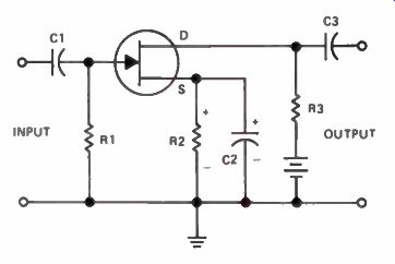
Figure 21. Schematic diagram of an amplifier using an n-channel JFET.
The waveforms in Fig.22 show how the circuit works. With zero input signal the drain voltage is constant, as shown in Fig.22(A). Figure 22(B) shows what happens when a signal is applied to the gate. With zero signal, the gate voltage is zero. When the positive half-cycle arrives, it swings the gate voltage positive as shown between points 1, 2, and 3. The peak voltage at point 2 must not exceed the positive voltage on the source or current flows to the gate, introducing distortion and possible damage to the transistor. During the next half-cycle the input signal swings the gate in a negative direction, as shown from point 3 to point 4 and back to point 5.
Figure 22(C) shows what happens to the voltage between the drain and ground. When the gate voltage swings in a positive direction it reduces the negative bias between the gate and channel, permitting the channel to widen. This widening reduces the resistance of the channel.
Current through the JFET increases so the voltage drop across R3 increases. When this hap pens, the net voltage between the drain of the JFET and ground decreases as shown from point 1 to point 2 and then back to point 3.
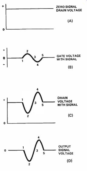
Figure 22. Waveform for the circuit In Fig.21.
During the next half-cycle, when the input signal swings negative, it increases the net negative bias between the gate and the channel. This causes the channel width to decrease, effectively increasing the resistance of the channel. As a result, the current through the JFET decreases, causing the voltage drop across R3 to decrease.
When this happens, the voltage between the drain and ground swings positive, as shown between points 3, 4, and 5 in Fig.22(C). Any amplified signal appearing at the output on the drain of the JFET takes the form of an amplified AC signal superimposed on the de drain voltage. At the output, on the other side of the blocking capacitor C3, we have the waveform shown in Fig.22(D). Here the DC is blocked so that the signal appears as an amplified signal.
Notice that the output signal is larger than the input signal. A relatively small signal applied to the input causes a variation in the current flowing through R3, which is a rather large resistor.
This develops an amplified signal voltage in the output. Also, notice that when the input signal swings in a positive direction, the output signal swings in a negative direction, and vice versa.
That is, the output signal is 180° out of phase with the input signal. Remember that this is the same situation that we encountered with the junction transistor in the common-emitter circuit.
P-Channel JFETs. In Fig.23 we've shown a schematic diagram similar to the one shown in Fig.21, but this time we've used a p-channel JFET. Remember that in a p-channel transistor, conduction through the transistor occurs by means of holes.
In this circuit, the positive terminal of the battery is connected through R2 to the source, so that electrons come out of the transistor from the source connection. This creates holes that travel through the channel to the drain, where they are filled by electrons traveling from the negative terminal of the battery through R3 to the drain.
The electrons leaving the source and flowing through R2 develop a voltage drop across R2 with the polarity indicated. This makes the source negative with respect to ground. Since the gate connects to ground through R1, the source is negative with respect to the gate. This is the same as saying that the gate is positive with respect to the source. If the gate is positive with respect to the entire channel, no holes flow from the channel to the gate and, therefore, no electrons flow through R1.
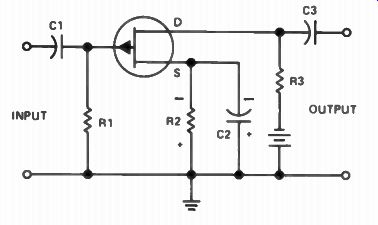
Figure 23. Schematic diagram of an amplifier using a p-channel JFET
The waveforms in Fig.24, on the next page, show what happens when the signal is applied to the input. With zero signal, the voltage between the drain and ground is constant and negative, as shown in Fig.24(A). Figure 24(B) shows that the gate voltage is constant and zero until a signal is applied to the input. When the input signal swings in a positive direction from point 1 to point 2 and then back to zero voltage at point 3, it increases the positive voltage on the gate. The increased voltage adds to the voltage across R1, making the gate more positive. This repels the holes into a narrower channel so the resistance of the channel in the JFET increases.
This reduces the number of holes traveling from the source to the drain so the number of electrons leaving the negative terminal of the battery and flowing through R3 to fill the holes arriving at the drain decreases. When this happens, the voltage drop across R3 decreases so the voltage between the drain and ground increases. In other words, the drain becomes more negative.
This is shown in Fig.24(C) as the drain voltage swings from zero signal voltage at point 1 to a more negative level at point 2, and then back to zero at point 3.
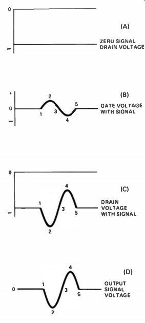
Figure 24. Waveforms for circuit shown in Fig 23.
During the negative half of the input signal, the gate voltage swings negative from zero at point 3 to a maximum negative value at point 4, then back to zero at point 5. This subtracts from the voltage across R1, making the net voltage between the gate and the source lower. The gate is less positive. The lower positive voltage has less repelling effect; thus the width of the channel increases, permitting more holes to flow through the channel from the source to the drain.
The increase in the number of holes arriving at the drain results in an increase in the number of electrons leaving the negative terminal of the battery and flowing through R3 to fill the holes that reach the drain. The increased current through R3 results in a greater voltage drop across R3. The drain voltage becomes less negative as the drain voltage swings from point 3 to a minimum at point 4 and then back again to zero signal level at point 5, as shown in Fig.24(C). Figure 24(D) shows the output signal once the DC voltage at the drain has been removed by the blocking capacitor C3. Compare this with Fig. 22(D) and you see that the two are identical.
In the p-channel JFET we have a voltage gain because the output signal is greater than the input signal. We also see that the output signal voltage is 180° out of phase with the input signal voltage.
Characteristics. There are several important characteristics of the JFET circuit that you should remember. Remember that the output signal is greater than the input signal because the small signal voltage causes a varying current to flow through a high value of load resistor developing a large output voltage. Also, remember that the output voltage is 180° out of phase with the input.
Consider the input circuit. Since the gate is reverse biased, there is little or no current flowing from the channel to the gate. This means that the applied signal voltage has little or no signal current flowing in the gate circuit. Therefore, the input impedance of the JFET is very high - usually several megohms. The output impedance is determined by the value of the load resistor, which is usually in the vicinity of 20k or more. Because of its very high input impedance, the JFET is particularly useful in applications where we must avoid loading the source voltage.
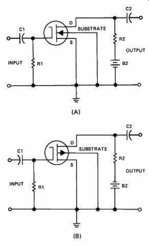
Figure 25. IGFET amplifiers using (A) an n-channel IGFET and (B) a p-channel
IGFET.
Insulated-Gate Field-Effect Transistors
Figure 25(A) shows a diagram of an amplifier using an n-channel, insulated-gate, field-effect transistor (IGFET), and Fig.25(B) shows an
amplifier using an p-channel, insulated-gate, field-effect transistor. Notice that in both circuits the source is connected directly to ground in stead of to ground through a resistor. This means that in both circuits there is no reverse bias applied to the gate. The gate is insulated from the channel and therefore there is no way electrons can flow from the channel to the gate, or from the gate to the channel. Thus reverse bias is not needed.
The operation of these circuits is the same as the operation of the JFET circuits. In both cases, the output signal is 180° out of phase with the input signal. The IGFET has an even higher input impedance than the JFET. This is due to the fact that there is some leakage across the gate-channel junction in a JFET because of the minority carriers crossing the junction. There is no leakage across the junction in an IGFET because there is an insulator between the gate and the channel. As a matter of fact, the input impedance of these devices is so high that manufacturers usually ship them to the user with the leads wrapped in tin foil or some other conducting device. This is to keep the gate shorted to the source or the drain so the gate cannot build up a high static charge. Since there is no way for this charge to dissipate, the charge can build up to such a high value that it punctures the insulation between the gate and the channel. Once this happens, the transistor is destroyed.
Dual-Gate MOSFETs
Earlier we mentioned that the MOSFET is a metal oxide semiconductor field-effect transistor. The metal oxide refers to the insulation used between the gate and the channel. The MOSFET can be made with a single gate or a dual gate.
Figure 26 is a diagram of an amplifier using a dual-gate, n-channel MOSFET. The input signal is applied to gate 1 as shown, and the output signal is taken off between the output terminals.
With gate 2 grounded, the input signal applied to gate 1 causes the current flowing through the channel to vary. This varies the voltage drop across R2 so that the voltage between the drain and ground varies and an output signal is produced.
If, instead of grounding gate 2, we apply a negative voltage to it, we can vary the gain of the transistor by varying the negative voltage. With zero voltage, a signal applied to gate 1 causes a certain varying current to flow through the channel. But if we apply a negative voltage to gate 2, it restricts the channel width so that the current decreases. This reduces the amplitude of the varying current flowing through the channel and hence the varying voltage developed across R2.
As a result, the output signal decreases. If we increase the negative voltage applied to gate 2 still further, the varying current continues to
decrease and the amplitude of the output signal in turn continues to decrease. In fact, if we make a negative voltage applied to gate 2 high enough, we can cut off the flow of current through the channel so that the output signal drops to zero.
The operation of the transistor is exactly the same as that of the JFET described earlier, except here we have a means of controlling the gain by varying the voltage applied to the gate. In the case of an n-channel transistor, we would apply a negative voltage to gate 2 in order to reduce the gain of the stage. In the case of a p-channel transistor, we would apply a positive voltage to the gate. Dual-gate MOSFETs are widely used as the RF amplifier in TV tuners. It is possible to vary the gain of the stage over a wide range with this type of FET so that on strong local stations, the RF stage amplifies the signal very little. This prevents overloading the receiver with a strong signal received from the local station. On the other hand, if you tune the TV receiver to a weak distant station, then the reverse bias applied to the gate automatically decreases and the stage operates with a maximum gain in order to amplify the weak signal as much as possible to provide a satisfactory picture. There are other applications where dual-gate MOSFETs are used to control the gain of the stage.
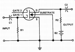
Figure 26. Amplifier circuit using a dual-gate MOSFET.
Review
There are two basic types of field-effect transistor - the junction-gate (JFET) and the insulated gate (IGFET). These field-effect transistors offer certain advantages over the bipolar transistors we discussed earlier in this lesson. Both have a very high input impedance, and in any circuit using an FET there is a 180° phase reversal.
One important type of IGFET that we have discussed is the MOSFET. Its operation is exactly the same as that of the JFET, except that, with a MOSFET, we can control the gain by varying the voltage applied to the gate. MOSFETs are widely used as RF amplifiers in TV tuners and computers.
Self-Test Questions
16 Is the amplified output signal from a field effect transistor in phase or out of phase with the input signal?
17 What potential must be applied to the gate of a p-channel JFET?
18 What important characteristic does the input impedance of a FET amplifier have?
19 Which has the higher input impedance, a JFET or an IGFET?
20 What purpose does gate 2 in a dual-gate MOSFET serve?
----------------------
TRANSISTOR CHARACTERISTICS
The table in Fig.27 is a summary of both bipolar and field-effect transistor characteristics. There are a number of important characteristics that you should remember. The common-collector type has a voltage gain less than 1; all other circuits provide a high voltage gain. The common-base circuit has a current gain less than 1, whereas all others provide a higher current gain. In the common-base and common-collector circuits, the output signal is in phase with the input signal. In all the other circuits, the output signal is 180° out of phase with the input.
There are a number of symbols used in describing transistor performance. Most of these symbols are of interest to circuit designers and engineers, but not to the technician. However, there are a few that are widely used that you should become familiar with. You may encounter them in your work.
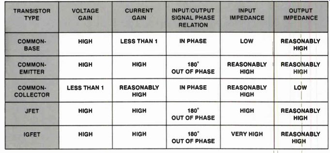
Figure 27. Bipolar and field-effect transistor characteristics.
Transistor Symbols
As you might expect, the letter I is used to represent current in transistor circuits. When the capital letter I is used, it indicates DC current or rms current. When the small letter i is used, it indicates the instantaneous current.
You frequently see references to the AC current in a transistor. When an AC signal is applied to the input of a transistor circuit, it causes the current in the output circuit to vary. We can consider the current in the output circuit as a de current with an AC current superimposed on it.
Remember that when we used a capacitor in the output circuit to block the DC voltage, we got a signal voltage that was strictly an AC voltage. If we connect a resistor across the output terminals, we have an AC current flow. It is important for you to remember that when we refer to AC current in a transistor, we are referring to the AC current that is, in effect, superimposed on the de current that flows through the transistor under zero signal conditions.
Currents flowing to or from the various transistor terminals are identified by means of a letter representing the terminal. For example, the emitter current is represented by the letter E or e. Base current is represented by B or b and collector current is represented by the letter C or c. Using these symbols, the de emitter current is designated by the symbol I E The rms emitter current is represented by the symbol l e, and the instantaneous emitter current is represented by the symbol i e. Similarly, dc base current is represented by I B, rms base current is represented by Ib, and instantaneous base current is represented by Ib. Collector DC current is represented by Ic, rms collector current is represented by lc, and instantaneous collector current is represented by i.
Two characteristics that are often referred to in transistors are the forward current and reverse current. The symbol used to represent the DC forward current is I F, and i F is used to represent the instantaneous forward current.
The DC reverse current is represented by I R, and the instantaneous reverse current is represented by iR. Remember that in normal operation a transistor is operated with forward bias across the emitter-base junction and reverse bias across the base-collector junction. Thus, in an NPN transistor, current can flow from the emitter, across the emitter-base junction, through the base, across the base-collector junction, through the collector, and to the positive terminal of the battery, placing the reverse bias across the base collector junction. However, there would be times when some minority carriers would cross the various junctions in a reverse direction.
Thus, there is a current flow across the base collector junction due to holes traveling from the collector across the junction into the base. This reverse current is kept as small as possible Because it is useless current. Transistor manuals often list the reverse current across the collector base junction. The current that is listed is the current that flows across the junction when the junction is reverse biased and the emitter is open circuited. This DC current is represented by the symbol Icl io The letters CB indicate that the current is across the collector-base junction in the reverse direction. The letter 0 indicates that the other electrode, the emitter, is open. This symbol is so widely used that it is often abbreviated Ico Groups of letters are used in this manner to indicate other transistor currents. For example, the symbol 'CEO is used to represent the DC collector current with the collector reverse-biased and the base open-circuited.
There are other symbols used in conjunction with the transistors, but you can usually figure out what the symbols mean. Transistor manuals and data sheets are also available from electronic parts distributors. Most of these manuals list all the symbols and tell you what they mean.
Current Gain
You already know that the current gain of a transistor used in a common-base circuit is rep resented by the Greek letter a, and the current gain in a common-emitter circuit is represented by the Greek letter p.
Frequently in transistor characteristics, you see the alpha cutoff frequency listed. Transistors are designed to operate up to a certain maximum frequency. The alpha cutoff frequency is the frequency at which the current gain of a transistor in a common-base circuit drops to approximately 70% of the gain that is listed in the transistor characteristics. The higher the alpha cutoff frequency, the higher the frequency at which the transistor can be used.
Manufacturers usually give either the alpha or the beta of a transistor, but seldom both.
Sometimes when the alpha is given, you want to know the value of beta and vice versa. If you know the alpha of a transistor, you can find beta from the formula: a 1 3= 1 - a
If you know the beta of a transistor, you can find the alpha from the formula: a = 3 1 +13
It is not necessary that you memorize these formulas, but try to remember where they are so you can look them up if you need them.
Review
Because transistors are used so frequently in electronic circuitry, it is very important that you get to know all the different types and their symbols. They come up often in your electronics studies and experiences. It is also important that you understand the information given on the table in Fig.27, as well as the formulas for deter mining current gain in transistors.
Self-Test Questions
21 What symbol is used to represent the DC base current?
22 What symbol is used to represent the rms collector current?
23 What symbol is used to represent the instantaneous-emitter current?
ANSWERS TO SELF-TEST QUESTIONS
1 Yes. In the common-emitter circuit, the signal voltage is applied across the input resistor. None of the emitter current that is flowing through the collector flows through this resistor. The actual signal current flowing in the input is comparatively small. At the same time, the collector current is equal to the emitter current minus any current loss at the base and is therefore much larger than the signal input current. As a result, a current gain is possible in the common-emitter circuit.
2 The amplified signal voltage is many times the input voltage and is 180° out of phase with it in the common-emitter circuit.
3 Figures 4 and 5 are schematics of a common-emitter circuit using an NPN transistor. Figure 6 is a schematic using a PNP transistor.
4 No. In the common-base circuit, the collector current is always less than the emitter current because part of the emitter current leaves the transistor through the base.
5 They are in phase.
6 We can obtain a voltage gain in a common base circuit because the output load resistor can be made quite large. Thus, even though the signal current flowing through the load is smaller than the input signal, the fact that the output load resistor can be made many times the input impedance of the transistor results in the output voltage being greater than the input signal voltage.
7 A very low input impedance and a high output impedance.
8 The output signal voltage is in phase with the input signal voltage.
9 The voltage gain of a common-collector circuit is always less than 1.
10 The common-collector circuit has a high input impedance and a low output impedance. Its input impedance is higher than that of the other two circuits, and it is the only circuit in which the output impedance is lower than the input impedance.
11 The common-emitter circuit.
12 The common-base circuit and the common emitter circuit.
13 The common-emitter circuit and the common-collector circuit.
14 The common-emitter circuit and the common-collector circuit.
15 The common-collector circuit.
16 180° out of phase.
17 A positive potential.
18 It has a high input impedance.
19 The IGFET has a higher input impedance than the JFET.
20 It can be used to control the gain of the MOSFET.
21 'B.
22 I c.
23 i e.
Lesson Summary
Some of the important facts that you should remember about this lesson are:
• The three basic amplifier configurations are common base, common emitter, and common collector.
• Either a PNP or an NPN transistor can be used in any amplifier con figuration.
• The current gain of a common-base amplifier circuit is an important characteristic that is represented by the Greek letter alpha.
• Current gain of a common-emitter amplifier circuit is represented by the Greek letter beta.
• Dual-gate MOSFETs provide a means of automatically controlling the gain of an FET amplifier circuit.
LESSON QUESTIONS
This is Lesson Number 2227.
Make sure you print your name, student number, and lesson number in the space provided on the Lesson Answer Form. Be sure to fill in the circles beneath your student number. Code the lesson number as shown at the right.
Reminder: A properly completed Lesson Answer Form allows us to evaluate your answers and speed the results and additional study material to you as soon as possible. Do not hold your Lesson Answer Forms to send several at one time. You may run out of study material if you do not send your answers for evaluation promptly.
1. The transistor with the highest input impedance is a(n):
a. PNP
b. NPN.
c. IGFET.
d. JFET.
2. The basic transistor circuit that does not provide a current gain is the:
a. Common-emitter circuit.
b. Common-base circuit.
c. Common-collector circuit.
3. The basic transistor circuit that does not provide a voltage gain is the:
a. Common-emitter circuit.
b. Common-base circuit.
c. Common-collector circuit.
4. Which basic transistor circuit provides a 180° phase shift?
a. The common-base circuit.
b. The common-emitter circuit.
c. The common-collector circuit.
5. The common-base circuit has:
a. The highest input impedance.
b. A current gain.
c. A low output impedance.
d. A voltage gain.
6. The common-emitter circuit provides:
a. A current gain.
b. A low input impedance.
c. A low output impedance.
d. An amplified in-phase voltage.
7. The common-collector circuit provides:
a. A low input impedance.
b. A high output impedance.
c. A voltage gain.
d. A current gain.
8. An amplifier using a field-effect transistor has a(n):
a. High input impedance.
b. Low input impedance.
c. Voltage gain less than 1.
d. Amplified signal in phase with the input signal.
9. A MOSFET is a(n):
a. NPN transistor.
b. PNP transistor.
c. JFET.
d. IGFET.
10. The purpose of a second gate in a dual-gate MOSFET is:
a. To increase the gain.
b. To increase the input impedance.
c. To control the gain.
d. To increase the output impedance.
----------------
NRI Schools
GET ALONG WITH PEOPLE
A national magazine recently published the results of a survey in which it asked several hundred successful men and women: "What single ability have you found to be most essential to your success?" Almost unanimously, the answer was: "The ability to get along with people." I'm sure you are already aware of the importance of this often under valued ability. But did you think of getting along with others as a skill? It is a skill; one that you can learn like any other.
To be successful in any field--technical, artistic, or commercial--you must be able to get along with other people. You must have the ability to work with others to achieve your common goals. You can only profit from your special talents and skills if other people are willing to come to you for your services, and people won't seek you out if they don't like you.
Keep this in mind in your daily life. Practice getting along with people. Notice the things people respond to and the things that "turn them off" There is always room for improvement in this area. As you go along, you will learn what many happy and successful people al ready know--that getting along with others is the single most important factor in gaining or keeping success.
--------------------------