AMAZON multi-meters discounts AMAZON oscilloscope discounts
TABLE OF CONTENTS
Introduction
How Monolithic Circuits Are Made
Summary
Basic Circuits
Voltage Regulation
The Differential Amplifier
Compound-Connected Transistors
A Dual-Differential Amplifier
Summary
Self-Test Questions
Digital Circuits
The Inverter
The AND Gate
The OR Gate
The NAND Gate
The NOR Gate
Negative Logic
Flip-Flops
Common ICs
Summary
Self-Test Questions
Answers to Self-Test Questions
Lesson Questions
-------------------
HOW MONOLITHIC CIRCUITS ARE MADE
The manufacturing of an IC begins with a bar of silicon to which an impurity, such as boron, is added to produce a p-type silicon material. This bar of silicon is then sliced into discs a few thousandths of an inch thick.
Called the substrate, the p-type silicon is the foundation on which ICs are made. Each disc may be several inches in diameter so that a large number of ICs can be built on each disc.
After the circuits are built, the discs are cut up to form individual ICs.
After the bar of silicon has been cut into discs, the discs are polished to a very smooth surface. On the top of the disc, a layer of n-type silicon is deposited. This layer is called the epitaxial layer, and it will eventually become the collector for the NPN transistors that will form part of the IC. Next, we grow a layer of silicon dioxide 4 over the top of the n-type crystal by heating the chip in an oxygen atmosphere. At this stage, a side view of the enlarged chip looks like Fig.1. (The drawing is out of scale; the chip will actually be only a few thousandths of an inch thick.) The layer of n-type silicon on top of the substrate and the layer of silicon dioxide are extremely thin.
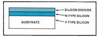
Figure 1. P-type silicon substrate with n-type epitaxia.
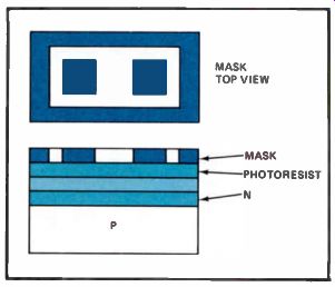
Figure 2. Drawing
showing mask and how it is placed layer and protective layer of silicon
dioxide. over silicon dioxide.
From here on, the procedure used depends on what elements are going to be formed on the substrate. If we are going to make an IC containing two NPN transistors, the next step is to coat the entire surface of the silicon dioxide with a photoresist material. This is the material that becomes chemically insolvent if it is exposed to ultraviolet light. After the silicon disc is coated with photoresist, a mask with opaque and transparent regions is made on film, as shown in Fig.2. The photo resist on the chip is then exposed to ultra violet light through the mask. At the spots where the mask is opaque, the ultraviolet light cannot go through and strike the photo resist. Where the mask is transparent, the light can get through and strike the photo resist. The chip is then rinsed in a developer.
Where light has not struck the photoresist, the developer removes the photoresist and exposes the surface of the silicon dioxide.
Next, the wafer is put into a chemical bath that etches or eats away holes, or windows, in the surface of the chip where it has not been exposed to the ultraviolet light. This action continues until the windows reach the n-type silicon, as shown in Fig.3. The silicon is then placed in an oven at high tempera ture, and the p-type silicon is diffused through the window in the n-type layer. The p-type material is diffused into the n-type material until it joins the substrate. There are now two areas of n-type material insulated from each other by the substrate and by the p-type material that has been diffused through the n-type material into the substrate. The chip now looks like Fig.4.
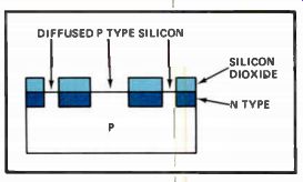
Figure 4. Drawing showing chip after p-type silicon is diffused through
the windows.
At this point, the entire surface of the chip is once again oxidized with silicon dioxide and then coated with photoresist. As shown in Fig.5, a new mask is then placed over the chip and once again the chip is exposed to ultraviolet light. Where the light strikes the chip, the silicon dioxide is protected by the photoresist, but where it is prevented from striking the chip by the opaque portion of the mask, the oxide and photoresist can be easily removed, forming new windows. P-type material is once again diffused into the windows forming the pn junctions that are shown in Fig.6.
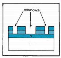
Figure 3. Windows are etched chemically down through the silicon dioxide
to the n region.
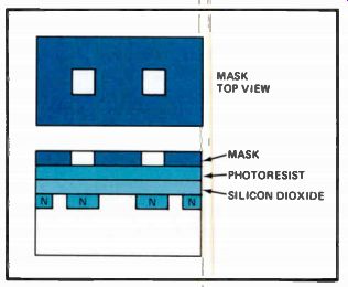
Figure 5. Drawing of the mask and chip ready for second exposure and
etching.
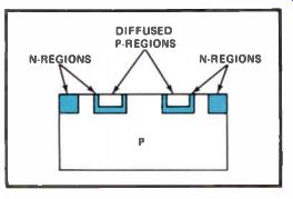
Figure 6. Drawing of chip after second p-type silicon diffusion.
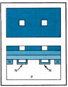
Figure 7. Drawing of mask and chip ready for third exposure.
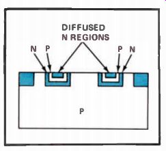
Figure 8. Drawing of chip after second n-type diffusion has formed two
NPN transistors.
Once again the surface is oxidized with sil icon dioxide and then coated with photo resist. As shown in Fig.7, another mask is placed over the chip. The chip is again ex posed to ultraviolet light and the opaque area of the mask is etched away. N-type material is then diffused through the windows, as shown in Fig.8, so that we now have two NPN transistors.
In the final step, windows are etched through a new mask through which aluminum is deposited to provide metal contacts for bonding leads to the transistor elements.
We have omitted a number of steps and many details in this description of how ICs are made, but the important thing to re member is that the transistors are formed in a series of steps, and since they are all formed at the same time, it is likely that they will have very similar characteristics. Al though the transistors formed by the procedures are NPN transistors, PNP transistors can also be formed using similar techniques.
You might wonder why the two transistors formed on the single p-type substrate do not short together through the substrate. This is easy to understand if you consider the operating voltages that will be applied to the transistor when it is in use. The larger n region that is first formed will be the collector of the transistors. The collector will have a positive voltage applied to it. The substrate will be at ground or zero potential.
Therefore, we have a reverse bias across the junction formed by the n-type collector and the p-type substrate, and no current can cross the junction. In other words, the n-type collector material and the p-type substrate act as a reverse-biased diode so that there will be no current flow across the junction.
The two transistors are thus isolated from each other by the substrate.
The two NPN transistors formed on the IC just described are bipolar transistors, so the IC is called a bipolar IC. There are other types of ICs that use insulated-gate field effect transistors.
You will recall that a MOSFET is an insulated-gate field-effect transistor in which the gate is a metal and is insulated from the channel by an oxide of the metal.
ICs using n-channel enhancement-type FETs are referred to as NMOS. ICs that use enhancement-type FETs where the channel is a p-type material are called PMOS. In some ICs, both enhancement-type n channel and p-channel FETs are used. In these ICs, the two FETs are connected in series and their gates are tied together.
When the voltage applied to the gate is positive, the n-channel FET can conduct; when the voltage applied to the gate is negative, the p-channel FET can conduct. These ICs are called CMOS, which means complementary metal oxides semiconductors.
There is another type of insulated-gate field-effect transistor IC that uses depletion type n-channel FETs. This type of IC is called HMOS. The ICs that use insulated-gate field-effect transistors have a very high impedance. It is possible for static charges of such high values to build up on the gates that the charge will break through the insulation and short the gate to the channel. This will destroy the IC. To prevent this from happening, when the IC is not in use, it should be plugged into a foam-type conductor so that the various leads on the IC will be shorted together.
Summary
You don't have to remember the IC manufacturing process, but remember that in a monolithic IC all the parts are formed by the same manufacturing pro cess. An IC using NPN or PNP transistors is called a bipolar IC. An NMOS IC uses n-channel enhancement-type FETs. A PMOS IC uses p-channel enhancement type FETs. A CMOS IC uses both n channel and p-channel enhancement type FETs. An HMOS IC uses n-channel depletion-type FETs.
-----------
BASIC CIRCUITS
There are two types of integrated circuits that are widely used today, digital ICs and linear ICs. In digital circuits, the various transistors are used in either the "on" or "off" state. In other words, the transistor is arranged so that it is either conducting at such a high level that it is saturated, or not conducting so that it is completely cut off.
In linear ICs, the transistors are biased at the midpoint of their characteristic curve.
Thus, in a linear IC, the linear transistors are capable of amplifying signals and producing an amplified version of the original signal in the input.
Voltage Regulation
Frequently, the successful operation of a circuit in an IC requires maintaining fairly close operating voltages on one or more stages within the IC. Often the voltage regulation is obtained by constructing one or more zener diodes within the IC. They are made at the same time, using the same processes used to form the transistors.
Zener Regulation. The circuit in Fig.9 shows how a zener diode can be used for voltage regulation. Here the input voltage applied to the circuit is 12 volts and the diode is maintaining the output voltage at 9 volts.
In a circuit of this type, the value of R1 is selected so that the normal current flow through it will produce a voltage drop of less than 3 volts. The current flowing through the diode supplies the additional current needed to maintain the output voltage at 9 volts. If the load current increases so that the voltage drop across R1 increases, the current through the diode decreases to maintain the output voltage at 9 volts. Similarly, if the load current decreases, the current through the diode will increase to keep the voltage constant.
The diode will also compensate for variations in the input of 12 volts. If the input voltage increases, the current through the diode will increase, so the voltage drop across R1 will increase to maintain the output voltage at 9 volts. Similarly, if the input voltage drops below 12 volts, the current through the diode will decrease, so the voltage drop across R1 will decrease to maintain the out put voltage at 9 volts.
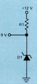
Figure 9. Zener diode voltage regulator circuit.
Notice that the input voltage must be greater than the required regulated voltage.
If the input voltage is 9 volts or less, the diode will not conduct and as a result we will not have any regulation.
Diode Regulation. Forward-based diodes can also be used as voltage regulators. A sil icon diode, when it is conducting, has a voltage drop of approximately 0.6 volt across it, which remains constant over a fairly wide current range. By arranging forward-biased diodes as shown in Fig.10, the voltage regulated by the series-connected diodes will be considerably higher than the voltage that could be regulated by a single diode.
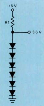
Figure 10. Forward-biased diodes used in a voltage regulator circuit.
Forward-biased diodes are widely used as voltage regulators in ICs. They are formed using the same processes that are used to form a transistor. Since the cathodes and an odes of the diodes are all formed at the same time, all of the diodes will have essentially the same characteristics. Therefore, the voltage drop across each diode is essentially the same.
In the circuit shown in Fig.10, six diodes, each with a voltage drop of 0.6 volt across it, are used to obtain a regulated voltage of 3.6 volts. You may encounter several strings of diodes, such as shown in Fig.10, in an IC where several regulated voltages are needed.
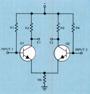
Figure 11. The basic differential amplifier circuit.
The Differential Amplifier
One of the most widely used amplifier circuits in linear ICs is the differential amplifier shown in Fig.11. Since the amplifier uses no capacitors, it can be used from DC up to vhf (very high frequency). Notice that the amplifier has two inputs, input 1 and input 2, and two outputs labeled E1 and E2. The output is taken between terminals E1 and E2. The greater the difference in voltage between the two input signals, the greater the output voltage. For example, let's see what happens if the input to Q1 swings in a positive direction and the input to Q2 swings in a negative direction.
The positive input to Q1 causes the current through the transistor to increase. This causes the voltage drop across R2 to increase so that the potential at El will swing in a negative direction. At the same time, the negative signal applied to the input of Q2 will cause the current through the transistor to decrease. As a result, the voltage drop across R3 will decrease, causing the potential at E2 to swing in a positive direction. Thus, we have E1 swinging in a negative direction and E2 swinging in a positive direction, so that considerable output voltage is developed between these two terminals. If the positive signal fed to the input of Q1 is equal to the negative signal fed to the input of Q2, and the transistors, as well as R2 and R3, are matched, the increased current through Q1 will be exactly offset by the decrease in current through Q2. As a result, the current through R5 will remain constant and the voltage drop across it will not change.
Note what happens when the two input signals of the amplifier are equal in amplitude and phase. If the inputs to Q1 and Q2 both swing in a positive direction, the current through both transistors will increase, increasing the voltage drop across both R2 and R3. As a result, El and E2 will both swing in a negative direction so that the net voltage difference between E2 and El will be zero. At the same time, the current through R5 will increase, increasing the voltage drop across it. Thus, the emitters of both transistors will swing in a positive direction. This will subtract from the positive signals fed to the two inputs. The current increase through the two transistors will be considerably less than it would be if the emitters were connected directly to ground. This limits the current increases through R2 and R3, resulting in very little change in the voltage between El and ground and E2 and ground. At the same time, the increase in the voltage drop across R5 further limits the change in voltage between El and ground and E2 and ground so that these two voltages remain essentially constant.
At the same time, any change in the voltage between El and ground and the voltage between E2 and ground will be equal so that there will be no voltage between E1 and E2.
Thus, the equal in-phase signals fed to the two inputs will not result in any output. This is referred to as common-mode rejection. It simply means that the amplifier will not produce an output signal if there are any changes in the operating voltage or stray signals picked up at the two inputs. Thus, hum or any other noise signal picked up by the two inputs will not result in an output signal. Common-mode rejection is an important characteristic of the differential amplifier; you should remember what it is.
The differential amplifier will also produce an output if there is only one input signal.
For example, if the input of Q1 swings in a positive direction, the current through this transistor will increase, causing the voltage drop across R2 to increase so that the potential at E1 will swing in a negative direction.
If there is no signal at the input of Q2, the increased current through Q1 will cause the voltage drop across R5 to increase. This will reduce the forward bias across the emitter base junction of Q2, causing the current through this transistor to decrease. As a result, the voltage drop across R3 will decrease, causing the voltage at E2 to swing in a positive direction. Therefore, we have an output signal that is once again equivalent to the difference between the voltages at E1 and E2.
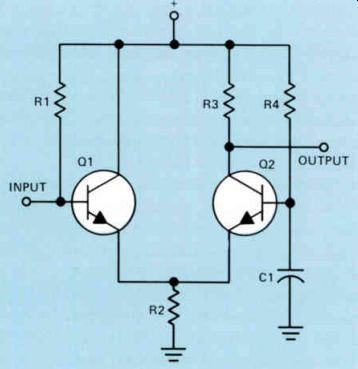
Figure 12. Modified differential amplifier circuit.
When used in ICs, the basic differential amplifier circuit is usually modified as shown in Fig.12. Notice that the collector of Q1 is brought directly back to the positive power supply. The base of Q2 is operated at signal ground potential by bypassing it to ground through C1. The term signal ground potential simply means that insofar as any input signal is concerned, the base of Q2 is connected directly to ground. The reactance of C1 is so low that insofar as a signal is concerned, the base of Q2 is connected directly to ground.
The input signal is fed to the base of Q1 and the output signal is taken from the collector of Q2. When the input signal causes the base of Q1 to swing in a positive direction, current through the transistor will increase, increasing the voltage drop across R2.
This will swing the emitter of Q2 in a positive direction, reducing the forward bias across the emitter-base junction of Q2. This will cause the current through the transistor to decrease, causing the voltage drop across R3 to decrease. Thus, the voltage between the collector of Q2 and ground will swing in a positive direction.
When the input signal applied to Q1 swings in the negative direction, it will re duce the current through the transistor, which in turn will reduce the voltage drop across R2. This will cause the forward bias across the emitter-base junction of Q2 to increase, increasing the current through the transistor and thus the voltage drop across R3. This means that the voltage between the collector of Q2 and ground will decrease or, in other words, swing in a negative direction.
Notice that there is no phase shift in this differential amplifier. For a positive-going input signal, we get a positive-going output signal; for a negative-going input signal, we get a negative-going output signal.
Constant-Current Circuit. Figure 13 is a diagram of an integrated circuit using a modified form of the differential amplifier.
Terminals 1 through 5 are terminals of the IC. The transistor Q3 is called a constant current sink or a constant-current source. By this we mean that the current through Q3 remains essentially constant. Let's see how this works.
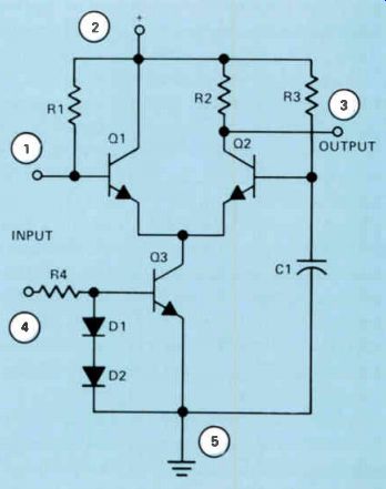
Figure 13. Differential amplifier with a constant-current sink
Notice that the connection from R4 goes to terminal 4 of the IC. A small positive voltage is applied to this terminal. Current will flow from ground through D2, D1, and R4 to terminal 4. The voltage drop across D1 and D2 will remain constant. If the voltage at terminal 4 increases slightly, the current through D1 and D2 will increase, as well as the current through R4. This will cause a greater voltage drop across R4 so that the voltage drop across the series-connected D1 and D2 will remain essentially constant.
Similarly, when the voltage at terminal 4 drops slightly, the current flow in the circuit will drop, so the voltage drop across D1 and D2 will remain constant.
As long as the voltage drop across D1 and D2 is constant, there will be a constant for ward bias across the emitter-base junction of Q3. As long as the forward bias across this junction is constant, the current flow through the transistor will remain constant.
If an input signal fed to terminal 1 swings positive, the forward bias across the emitter base junction of Q1 will increase and the current through this transistor will increase.
Since Q3 is supplying emitter current for both Q1 and Q2, and the current through Q3 is constant, if the current through Q1 increases, the current through Q2 must decrease. If the current through Q2 decreases, the voltage drop across R2 will decrease and the output at terminal 3 will swing in a positive direction.
If the input signal drives terminal 1 in a negative direction, the forward bias across the emitter-base junction of Q1 will decrease and the current through Q1 will decrease.
Again, since the current through Q3 is constant, the current through Q2 must increase.
The voltage drop across R2 will increase so that the voltage at the collector of Q2 will decrease and the voltage at output terminal 3 will swing in a negative direction. Notice that with this circuit we once again have an output signal that is in phase with the input signal.
DC Level Shifting. If we need more gain than we can get from a single amplifier, a second differential amplifier can be used.
However, in both Figs.12 and 13, the DC out put voltage at the collector of Q2 is considerably higher than the base voltage at the input of Q1. Therefore, rather than trying to direct-couple the second differential amplifier, an emitter-follower stage is used between the two to get the DC voltage down to a lower level. Then, a second differential amplifier can be driven quite conveniently.
The circuit used to lower the DC level is shown in Fig.14. Notice that in this circuit, Q1 and Q2 form a differential amplifier that is identical to the circuit shown in Fig.12.
The output from Q2 is coupled directly to the base of Q3, and the output signal is taken from the emitter of Q3. By controlling the characteristics of Q3 and the size of R5, we can obtain the correct DC voltage at the emitter of Q3 to correctly bias the base of the first stage of a second differential amplifier.
Figure 14. A differential amplifier and an emitter-follower stage.
In some integrated circuits, you will find two or three differential amplifiers and an emitter follower connected in cascade, which means that one differential amplifier is connected after another. The differential amplifiers are isolated from each other by an emitter-follower stage that lowers the DC level, so that in each case the output from the emitter follower provides the correct forward bias for the first stage of the following differential amplifier.
Very high gain can be obtained by using two, three, or more cascaded stages, as shown in Fig.14. If three differential amplifiers with an emitter-follower output are used in an integrated circuit, and each differential amplifier and emitter follower provides a gain of 10, the total gain of the three cascaded stages will be 10 x 10 x 10 = 1000. It is relatively easy to obtain a gain of 10 in each differential amplifier and emitter follower stage of this type.
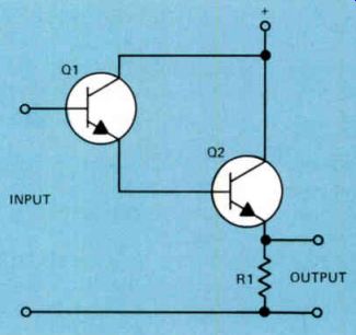
Figure 15. A compound-connected emitter-follower circuit.
Compound-Connected Transistors
An example of a compound-connected emitter follower is shown in Fig.15. This type of circuit is frequently called a Darlington circuit. Two important characteristics of this type of circuit are a very high current gain and a relatively high input impedance.
Notice that in the circuit shown in Fig.15, the base current of Q2 is the emitter current of Q1. Thus, with similar transistors the base current of Q1 will be much lower than it would be if it were connected in the conventional common-emitter or emitter follower circuit. A relatively small change in the base current of Q1 will produce a large change in the emitter current of Q2.
The relatively high input impedance of the Darlington circuit is due to the low base current of Q1. In a typical transistor, 95% of the emitter current will flow through the collector and 5% will flow through the base.
Thus, in Q2, only 5% of the emitter current flows through the base. If Q1 has similar characteristics, 95% of its emitter current will flow through the collector. Since 95% of 5% is 4.75%, this leaves only 0.25% of the emitter current of Q2 to flow to the base of Q1. The base current of Q1 will be much lower than that of a single transistor stage.
Hence, we have a higher input impedance, and since the circuit behaves as a normal emitter follower, it will have a low output impedance.
The relatively small base current of Q1, compared to the emitter current of Q2, results in a higher overall gain. Thus, the stage has two important characteristics: a high current gain and a relatively high input impedance.
Compound-connected transistors are used not only in emitter-follower circuits, but also in compound-connected differential amplifiers, as shown in Fig.16. The gain of an amplifier of this type is considerably higher than the gain of the differential amplifier shown in Fig.11.
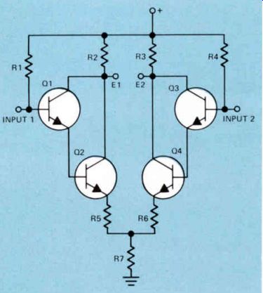
Figure 16. A compound-connected differential amplifier.
In the circuit shown in Fig.16, when an input signal drives input 1 in a positive direction, the small increase in the base current of Q1 will cause a larger increase in the emitter current of Q1. Since the emitter current of Q1 is the base current of Q2, the base current of Q2 must increase substantially.
An increase in the base current causes a large increase in the emitter current of Q2 and the collector current. Thus, we have the collector current increasing, which increases the voltage drop across R2 so that E1 will swing in a negative direction.
If at the same time there is a negative voltage at input 2, the negative voltage will cause the base current of Q3 to decrease. This decrease in base current will cause a much greater decrease in the emitter current, which in turn will cause the base current of Q4 to decrease. This will cause a large decrease in the collector current of Q4. Since both the collector currents of Q3 and Q4 decrease, there will be a considerable decrease in the voltage drop across R3 so that E2 will swing in a positive direction.
The signal voltage developed between terminals E1 and E2 of the compound differential amplifier will be much greater than it would be with a differential amplifier using only two transistors, because in this circuit all four transistors are amplifying the input change. This type of circuit can be used advantageously in an integrated circuit Because we can get a nearly perfect balance in the two amplifiers. For example, since all four transistors are formed at the same time, they should have practically identical characteristics. Similarly, it is possible to make R1 equal to R4, R2 equal to R3, and R5 equal to R6. This means that a given input applied to input 1 will produce the same change in El that the same input signal fed to input 2 will produce at E2.
A Dual-Differential Amplifier
The schematic diagram of an RCA type CA3026 IC is shown in Fig.17. It contains two differential amplifiers, each with a constant-current sink. Notice that there are no resistors or other parts in the IC except the transistors used in the differential amplifiers and the transistors used as current sources. The emitter of Q6, which is connected to terminal 9, is also connected to the metal case of the IC and to the IC substrate.
Also notice that there are no circles drawn around the transistors. It is common practice to omit the circles around the transistors and diodes in the schematics of ICs. This indicates that they are not discrete or separate components, but are a part of an integrated circuit.
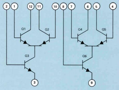
Figure 17. Schematic of a dual differential amplifier, type CA3026 IC.
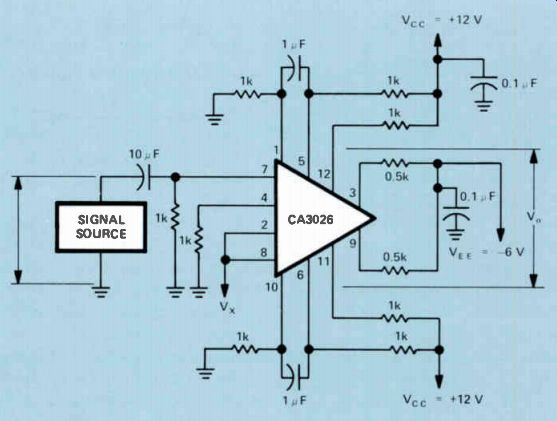
Figure 18. Using the CA3026 as a two-stage amplifier.
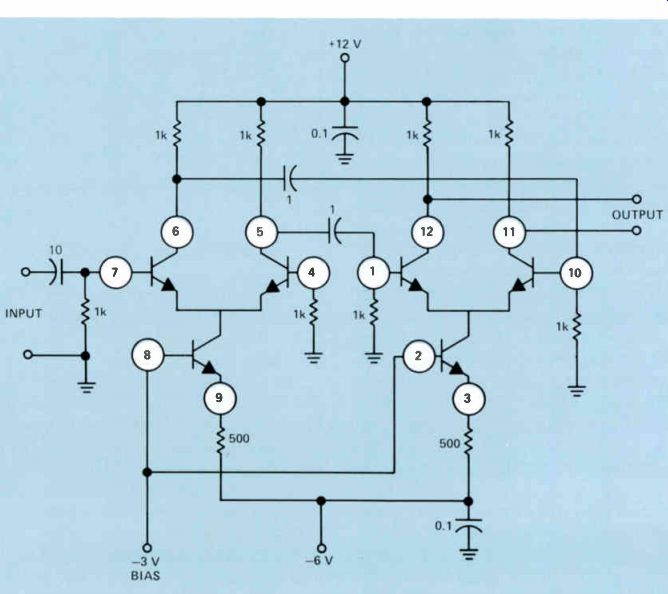
Figure 19. Complete schematic of the CA3026 two-stage amplifier.
Figure 18 shows how this IC can be used as a two-stage amplifier. This is the type of diagram you'll see when ICs are used as two stage amplifiers. As you can see, without knowing what is inside the IC it is difficult to trace out the circuit. However, by referring to Fig.17, which shows what is inside the IC, and to Fig.19, which shows the complete schematic of the two-stage amplifier, you should be able to trace out the circuitry shown in Fig.18.
Looking at Fig.18, we see that the input signal is fed to terminal 7. Figure 17 tells us that pin 7 is the base of Q4. The other transistor in this differential amplifier is Q5 and the base of this transistor is connected to pin 4. We see that pin 4 is connected to ground through a 1k resistor. If the input signal fed to pin 7 swings in a positive direction, the current through the transistor must increase. Since there is a constant-current source (Q6), the current through the other transistor in the differential pair (Q5) must decrease. As a result, we have a push-pull output between terminals 5 and 6. The term push-pull means that as the voltage at one terminal swings in a positive direction, the voltage at the other terminal is swinging in a negative direction.
The outputs from terminals 5 and 6 are then fed through the le coupling capacitors to the bases of the other differential amplifier pair, where the signal is amplified further by this pair. The amplified push-pull output will be present at terminals 11 and 12 of the second differential amplifier, which is the output.
The bases of the transistors used as constant-current sources are brought to external connections, so different values of base bias can be applied to the bases, depending upon the application. In the example shown in Fig.19, a voltage of - 3 volts is applied to pins 2 and 8 of the IC. When the IC is used as a two-stage amplifier, there will be a voltage gain of about 1000. To give you an idea of how much gain this actually represents, if we feed a 1 microvolt signal (in other words, a signal having an amplitude of 1 millionth of a volt) into terminal 7, we will have an amplified signal of 1000 microvolts, which is equal to 1 millivolt, between the output of terminals 11 and 12. If we take a second CA3026 and feed the output from terminals 11 and 12 of the first IC into terminals 4 and 7 of the second IC, with the circuit essentially the same as in Fig.18, we can get another voltage gain of 1000. Therefore, at terminals 11 and 12 of the second IC, the amplitude of the signal will be 1 volt. In other words, by connecting two ICs in cascade so that the signal is amplified first by one and then by the other, we can amplify the signal from 1 microvolt to 1 volt, getting a total gain of 1,000,000. You might wonder how large the CA3026 IC actually is. This IC is housed in what is called a TO-5 case. The drawing in Fig.20(A) gives the dimensions of the case. Notice that the maximum diameter of the rim of the case is 0.370 inch, or considerably less than one half inch.
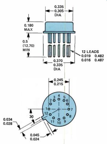
Figure 20. Physical layout of CA3026.
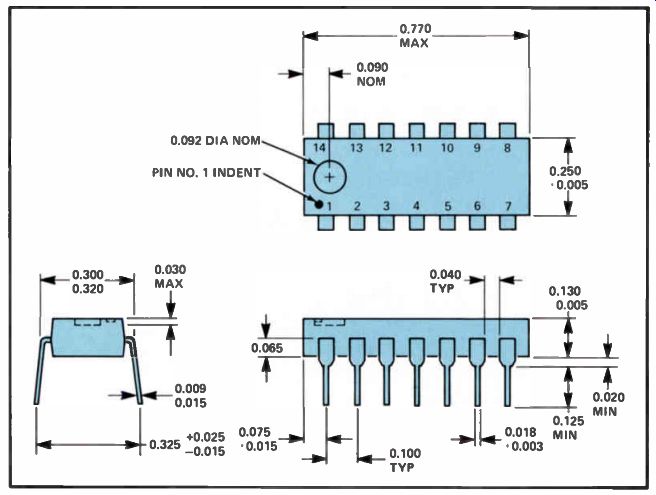
Figure 21. TO-116 case dimensions.
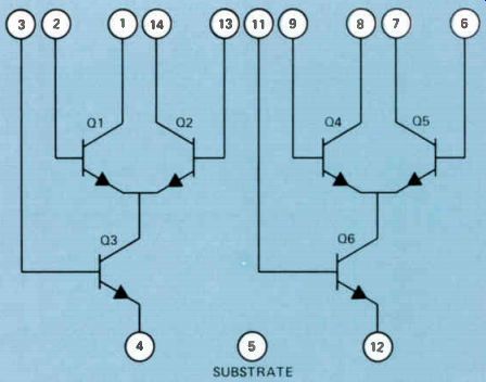
Figure 22. Pin connections for the CA3054 IC.
The various leads are identified by means of a small tip on the rim of the case adjacent to lead 12, as shown in Fig.20(B). Notice that there are 12 leads on this IC and lead No.12 is in the exact center of the tip on the rim.
This is a bottom view. Counting from lead 12 in the clockwise direction, we come to leads 1, 2, 3, and so on.
The CA3026 dual-differential amplifier is also available as the type CA3054 in a pack age that is called a 14-lead, dual in-line package, identified as a TO-116 package. The physical dimensions of this package are shown in Fig.21. Notice that there are 7 leads on each side of the package. Also notice the notch, called an index point, at one end of the package. This enables us to identify the various pins. The view that shows the notch is a top view, so looking at the IC with the notch to your left, the pin below and to the left is terminal 1, and the pin above and to the left is terminal 14. Notice that the pins on one side of the IC are numbered 1 through 7, and the pins on the other side are numbered 8 through 14.
Most of the ICs you will encounter will be in dual in-line packages. The number of pins will vary from 8 on up. The same numbering scheme is used on all in-line packages. For example, in the case of a dual in-line package with 24 leads, the terminals on one side will be numbered 1 through 12 and those on the other side will be numbered 13 through 24.
Figure 22 is a drawing showing how the dual-differential amplifiers are connected in the CA3054 IC. The differential amplifiers in this IC are electrically identical to those in the CA3026 IC, but as you can see the pin connection arrangements are quite different.
Summary
Some ICs have voltage regulators built in them. The voltage regulator may be a zener diode or it may be a group of conventional silicon diodes connected in series. A forward conducting silicon diode has a voltage drop of about 0.6 volt across it.
If you have a differential amplifier using two NPN transistors and the signal fed to the base of one swings in a positive direction, the voltage at its collector will swing in a negative direction. If the signal fed to the input of the other transistor swings in a negative direction, the voltage at its collector will swing in a positive direction. The output voltage is the difference in voltage between the two collectors. If equal amplitudes in phase signals are fed to the bases of the two transistors, the collector voltages will swing in the same direction, so the output will be zero.
The differential amplifier can be modified to use a single input and a single output. The differential amplifier is followed by an emitter-follower in order to reduce the DC voltage level at the output of the amplifier. Differential amplifiers and emitter-followers can be cascaded to obtain very high gain amplifiers. The transistor, with its base voltage held constant by means of the zener diode, forms a constant-current source.
A constant-current source is often referred to as a current sink.
Two important characteristics of a compound-connected emitter-follower, often referred to as a Darlington circuit, are a very high current gain and a relatively high input impedance.
Self-Test Questions
1 When a zener diode is used as a voltage regulator, is it forward biased or reverse biased?
2 If five forward-biased diodes are used as a voltage regulator and the voltage drop across one diode is 0.6 volt, what is the total regulator voltage?
3 When forward-biased diodes are used as a voltage regulator in an integrated circuit, why are the di odes likely to have identical characteristics?
4 If a differential amplifier, such as the one shown in Fig.11, is designed to provide a voltage gain of 10 in each stage, and a 1 volt positive signal is applied to both inputs, what will the output voltage be?
5 In the differential amplifier shown in Fig.12, will the output signal be in phase or 180° out of phase with the input signal?
6 What is the purpose of Q3 in the differential amplifier of Fig.13?
7 What purpose does Q3 serve in the circuit shown in Fig.14?
8 Give two advantages of the compound-connected emitter follower circuit over the emitter follower using a single transistor.
9 Why might compound-connected transistors be used in a differential amplifier?
10 In the ICs shown in Fig.17, which transistors are constant-current sources?
11 What type of circuits are contained in the ICs shown in Fig.17?
12 In the circuit shown in Fig.18, do we have a single-ended input or a push-pull input?
13 In the circuit shown in Fig,18, do we have a single-ended output or a push-pull output?
14 Is the maximum diameter of the type TO-5 case greater than or less than one-half inch?
15 How can you identify the various pins of an IC using a type TO-116 case?
16 In a 24-lead, dual in-line IC pack age, what pin will be at the same end as and opposite pin 1?
----------
DIGITAL CIRCUITS
Linear circuits are used to amplify the signal when we want the amplified circuit to be an exact copy of the original input. For ex ample, if a signal like that shown in Fig.23(A) is fed to a linear amplifier, the out put will be like Fig.23(B). The output is the same, but it is greater in amplitude.
A digital circuit has only two output conditions: maximum positive output and zero out put. If we feed a signal such as shown in Fig.23(A) to a digital circuit that requires a positive signal to produce an output signal, we will get an output like that shown in Fig.23(C). If we feed a signal like that shown in Fig.23(A) to a digital circuit that requires a negative voltage to produce an output, we will get an output like that in Fig.23(D). Again, notice there are only two output levels: maximum positive and zero.
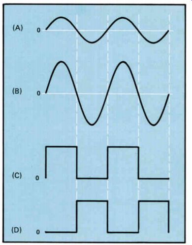
Figure 23. A comparison of signals from a linear circuit and a digital
circuit.
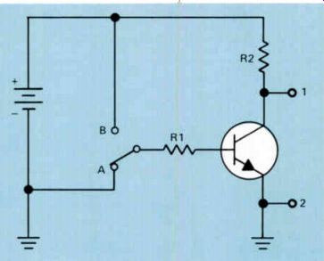
Figure 24. A transistor switch that produces binary outputs of 1 and
0.
Digital circuits are widely used in computers and microcomputers. Both use a numbering system called a binary system. In this system there are only two digits, 1 and 0. Thus, in a digital system, full output can rep resent 1 and zero output can represent 0. This might seem a little complex at first, but it is really quite simple. For example, look at the circuit shown in Fig.24. With the switch in the position shown, there is no for ward bias across the emitter-base junction of the transistor. Therefore, there will be no current flow through the transistor or through R2. Thus, if we measure the voltage on output terminal 1, the voltage will be positive and it will be equal to the full battery voltage. This might represent binary 1.
Now, when we throw the switch into position B, the base will be connected to the positive end of the battery through R1. This places a positive voltage on the base of the transistor, so the transistor will conduct heavily. It will go into what we call saturation, meaning it will conduct all the current it is capable of conducting. As a result, the transistor acts as a very low resistance between the emitter and the collector, while R2 is a comparatively large resistance.
Therefore, the voltage drop across the transistor will be practically zero, whereas al most the entire battery voltage will be dropped across R2. The voltage on terminal 1 will now drop to near zero. This condition represents a binary 0. This system of representing the digits 1 and 0 is called digital logic. The circuits used for this purpose are called digital logic circuits or simply logic circuits. When 1 is rep resented by the most positive voltage in the circuit, we have what is called positive logic.
In positive logic, we often refer to 1 as a high and 0 as a low.
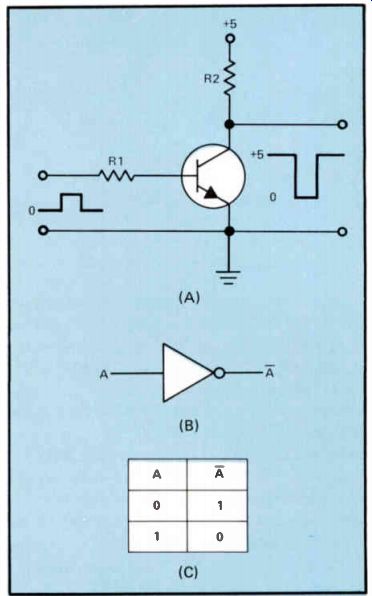
Figure 25. (A) A typical inverter circuit, and (B) its symbol. (C) A
logic table.
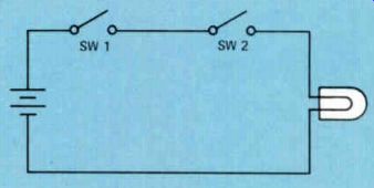
Figure 26. An example of an AND gate.
The Inverter
The schematic diagram of an inverter used with positive logic is shown in Fig.25(A). The inverter does exactly what the name implies: it inverts the signal. When the input is zero, the transistor will not conduct because there is no forward bias across the emitter-base junction. The output will be +5 as shown.
When the input swings positive, the transistor will saturate and practically the entire 5 volts will be dropped across R2 so that the output voltage will drop to zero. When the input signal drops back to zero, the transistor will stop conducting and the output will climb again to + 5 volts.
Figure 25(B) shows the symbol used to rep resent a logic inverter. The triangle represents some form of active circuit, such as a transistor, and the small circle indicates in version. The input A is at either a 1 or a 0 binary level. The output is À, which is read NOT A. This means that if the input is A, the output is NOT A; it is the inversion of A. We summarize this in a table called a truth table, which is shown in Fig.25(C). Where the input is zero, the output is NOT 0; it is 1. When the input is 1, the output is NOT 1; it is O. The AND Gate A gate is a circuit that looks at two or more binary signals and produces a binary output signal that depends upon the input signals.
An AND gate is a gate with two or more inputs that will produce a binary 1 output signal only when there is a binary 1 input signal at each input.
Figure 26 is a simple example that demonstrates AND gate operation. You can see that with either SW1 or SW2 open, or with both SW1 and SW2 open, the lamp will not light.
The only condition under which the lamp will light is when both switches are closed.
A semiconductor AND gate is shown in Fig.27(A). To see how this gate works, we will apply a logic level 0 to either input by grounding the input. We will apply a logic level 1 by connecting the negative terminal of a 6 volt battery to ground and the positive terminal to the input to which we wish to apply a logic level 1.
If we ground both terminals A and B to apply a logic 0 to each input, current will flow from ground to terminal A and through D1 and R1 to + 12 V. Current will also flow from ground to terminal B and through D2 and R1 to + 12 V. Since the conducting di odes will have practically zero resistance, almost the entire 12 volts will be dropped across R1, so the output at C will be zero.
If we connect the positive terminal of the 6 volt battery to input A, and keep input B grounded, current will still flow from ground to input B and through D2 and R1 to + 12 V. The voltage drop across D2 will be practically zero, so the voltage at output C will be zero.
If we ground input A and connect the positive terminal of the battery to input B, current will still flow from ground to input A and through D1 and R1 to + 12 V. The voltage drop across D1 will be practically zero, so the voltage at output C will be zero.
If we connect a 6 volt battery between ground and each input terminal, current will flow from ground through the battery to in put A and through D1 and R1 to +12 V. Current will also flow from ground through the 6 volt battery to input B and through D2 and R1 to + 12 V. The voltage drop across D1 and D2 will be practically zero, but since in puts A and B are now connected to + 6 volts, the voltage at C will be + 6 V, which represents a binary 1.
In Fig.27(B), we've shown two signals applied to inputs A and B and the output they will produce at output C. Notice that there is a binary 1, represented by the positive voltage at the output of C, only when there is a binary 1 present at both inputs A and B. At all other times, the output at C is zero.
The symbol for an AND gate is shown in Fig.27(C). Notice that we have used the mathematical expression C = AB to designate the AND operation. The gate output is designated C and the inputs are designated A and B. The equation tells us that the out put C occurs when both A and B are present.
The truth table for an AND gate is shown in Fig.27(D). Notice that when we have bi nary 1 at inputs A and B, we have a binary 1 at output C. With all other combinations, the output will be 0 at C. Only when we have a binary 1 at A and B will we have a binary 1 at C.
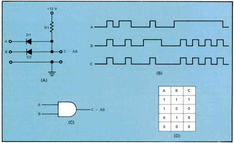
Figure 27. (A) The schematic symbol of a diode AND gate, and (B) the
input and output signals. (C) The symbol for an AND gate, and (D) the
truth table.
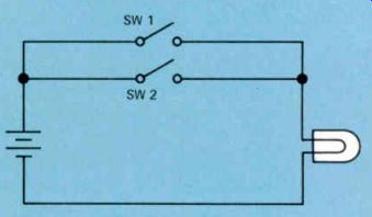
Figure 28. An example of an OR gate.
AND gates are not limited to two inputs.
We could have three or more inputs. If, for example, we have four inputs, the only time we'll get a binary 1 at the output is when we have a binary 1 at all four inputs.
The OR Gate A simple example of an OR gate is shown in Fig.28. Here, if we close switch 1, the light will light. If we leave switch 1 open and close switch 2, the light will also light. In other words, the light will light if either switch is closed. The light will also light if both switches are closed. The important thing to note it that the light will light if either switch 1 or 2 is closed.
The schematic diagram of a diode OR gate is shown in Fig.29(A). To see how the circuit works, we will do the same for logic level 0 and 1 as we did with the AND gate. For 0, we'll ground the input terminal. For 1, we'll connect the negative terminal of the 6 volt battery to ground and the positive terminal to the input to which we wish to apply logic level 1.
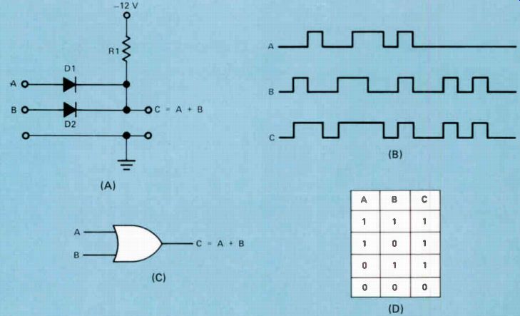
Figure 29. (A) A schematic diagram of an OR gate, and (B) input signals.
(C) The symbol for the OR gate, and (D) the truth table.
With logic level 0 applied to both inputs A and B (that is, both inputs grounded), diodes D1 and D2 will be forward biased because their cathodes are connected to the minus side of the supply through R1. Current flows from the negative side of the supply through R1, through D1 and D2 to ground, and to the positive terminal of the 12 volt supply: Since the resistance of the conducting diodes is practically zero, the voltage at output C will be zero, and the output is a binary zero.
With one input at ground and the other at logic level 1, the output, C, will also be at logic level 1. Let's see why this is so.
Let's apply a logic level 0 to input B by grounding it, and a logic level 1 to input A by connecting the negative terminal of the 6 volt battery to ground and the positive terminal to input A. This will place a total of 18 volts across D1 and R1 in series. D1 will conduct, and since the diode is practically zero resistance when it is conducting, the junction of the cathode of DI and the cathode of D2 and R1 will be at + 6 volts. This is a binary level 1, so we'll have a binary 1 at output C. Diode D2 can't conduct because it has a re verse bias of 6 volts across it. The cathode will have + 6 volts applied to it, and the an ode is at zero.
If input A is grounded and input B has + 6 volts applied to it, diode D2 will conduct, bringing terminal C to + 6 volts. In this case, D1 will be reverse biased and will not conduct.
If + 6 volts is applied to both terminals A and B, both diodes will conduct, again bringing terminal C to the + 6 volt or logic 1 level.
Notice the difference between the AND gate and the OR gate. With the AND gate, we had a logic level 1 at the output only when we had a logic level 1 at A and B. With the OR gate, we had a logic level 1 when we had a logic level 1 at either A or B (or both). Figure 29(B) shows input signals applied to inputs A and B and the output produced at terminal C. Figure 29(C) is the symbol used for an OR gate. Notice the mathematical expression C = A + B used to represent the OR gate. This is read C = A or B. The truth table for the OR gate is shown in Fig.29(D). The NAND Gate When an AND gate is followed by an inverter, it becomes a NAND gate. The word is derived from the words NOT and AND, where the NOT refers to the inverter and the AND refers to the gate. In Fig.30(A), we have shown an AND gate followed by an inverter.
Notice the mathematical output term AB; it means that the output produced is inverted.
The schematic symbol used to represent a NAND gate is shown in Fig.30(B). The truth table for the NAND gate is shown in Fig.30(C). Notice that the NAND gate output is exactly the opposite of an AND gate. This is because the inverter inverts the output from the AND gate.
The NOR Gate When an OR gate is followed by an inverter, as shown in Fig.31(A), we have a NOR gate. As you might expect, the name is de rived from the words NOT and OR. The mathematical expression for the output is read C = NOT A or B. The schematic symbol for the NOR gate is shown in Fig.31(B). The truth table for the NOR gate is shown in Fig.31(C). The output is opposite of that of an OR gate because the gate is made up of an OR gate and its output is then inverted.
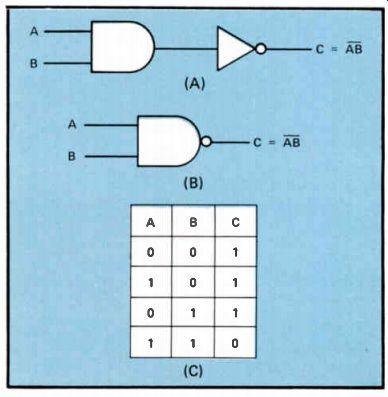
Figure 30. (A) An AND gate followed by an inverter be comes a NAND gate.
(B) The schematic symbol, and (C) the truth table.
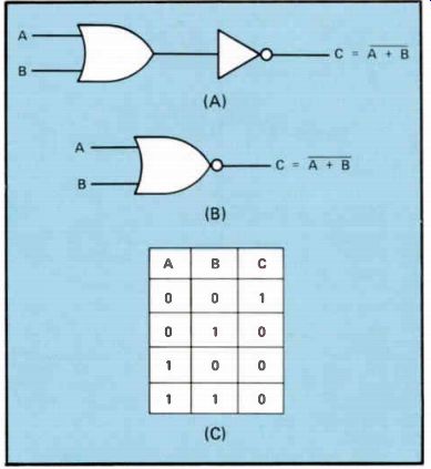
Figure 31. (A) An OR gate followed by an inverter be comes a NOR gate.
(B) The schematic symbol for a NOR gate. and (C) the truth table.
You might wonder why we need NAND and NOR gates. One reason is that in diode AND, and OR gates there is no amplification.
If the logic signal has to pass through several gates, its amplitude will decrease as it goes through each gate, and the system will be come unreliable. By using a diode gate followed by a transistor inverter, we can amplify the signal after it goes through the gate and thus maintain our logic level constant.
Gates such as NAND and NOR gates in which diodes and transistors are used are referred to as diode transistor logic, abbreviated DTL. In some logic circuits, you will find transistor gates and transistor inverters. This configuration is referred to as transistor-transistor logic, abbreviated TTL. Both DTL and TTL logic is used, but most modern logic gates use CMOS. We need not be concerned with the type of circuitry inside the gate; the main thing to remember is the function that the gate performs.
Negative Logic
The logic we have been discussing thus far is called positive logic. This means that a binary 1 is represented by a voltage that is positive with respect to binary 0. In the examples we've discussed, we've used + 6 V as binary 1, and 0 as binary 0. Another type of logic that you will some times encounter is negative logic. In negative logic, the voltage representing logic 1 is negative with respect to the voltage representing binary 0. With this logic, binary 1 could be 0 volt, and binary 0 could be + 6 V. Binary 0 could be 0 V and binary 1 could be - 6 V Notice the important difference here: In both examples given, binary 1 is represented by a voltage level that is negative with re spect to binary 0. The schematic symbol for a negative logic AND gate is shown in Fig.32(A). Figure 32(B) is the truth table for the negative logic AND gate. Notice that the truth table is the same as the truth table for the positive logic AND gate. Regardless of whether positive or negative logic is being used, to get a binary 1 in the output of the AND gate you must have a binary 1 at both inputs. The circuits for the two gates will be different, but they perform the same function.
Figure 33(A) shows the schematic symbol for the negative logic OR gate, and Fig.33(B) is the truth table for the negative logic OR gate. Notice that with this gate, you'll get a binary 1 in the output if you have a binary 1 on either or both of the two inputs. This is the same as for a positive logic OR gate.
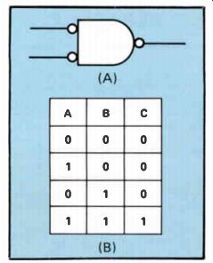
Figure 32. (A) The schematic symbol for a negative logic AND gate, and
(B) the truth table.
Let's go back and look at the gate shown in Fig.27. Remember that when we discussed this gate previously, we said that we'd use + 6 volts as one binary level and zero volts as the other. With 0 volts at either input, we had 0 in the output. The only time we got + 6 V in the output was when we applied + 6 V to both inputs. With negative logic, where 1 is represented by 0 volts and 0 is represented by + 6 V, we get a logic level 1 (0 volts) at C when either A or B, or both, are grounded.
We get a logic level 0 (+6 volts) only when +6 volts (logic level 0) is applied to both inputs. This means that with negative logic, the diode gate shown in Fig.27, which worked as an AND gate with positive logic, will function as an OR gate with negative logic. Similarly, the diode gate shown in Fig.29, which functions as an OR gate with positive logic, will function as an AND gate with negative logic.
Negative logic can be used with the gates shown in Figs.30 and 31. When negative logic is used with the circuit shown in Fig.30, the AND gate becomes an OR gate and the inverter performs the NOT function, so we have it performing the NOR function. The symbol for the negative logic NOR gate is shown in Fig.34(A). Similarly, when the circuit shown in Fig.31 is used with negative logic, the OR gate becomes and AND gate and the output is inverted by the inverter, so the inverter performs the NAND function.
The symbol for the negative logic NAND gate is shown in Fig.34(B). Table 1 is a summary of the logic symbols and truth tables for the logic gates discussed so far.
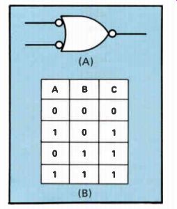
Figure 33. (A) The schematic symbol for a negative logic OR gate, and
(B) the truth table.
Figure 34. (A) The symbol for the negative logic NOR gate, and (3) the symbol for the negative logic NAND gate.
TABLE I --- A SUMMARY TABLE OF LOGIC SYMBOLS AND TRUTH TABLES
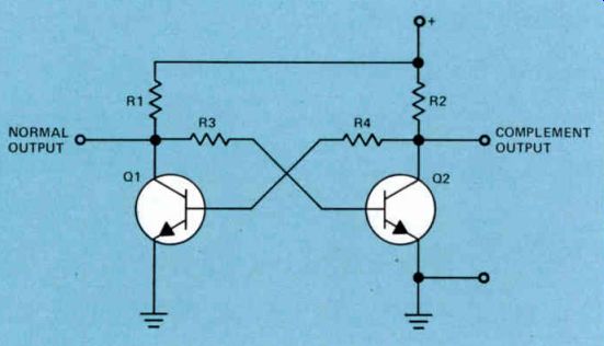
Figure 35. A flip-flop circuit.
Flip-Flops
Another important logic circuit is the flip flop. The circuit is called a flip-flop because it flips and flops between two stable states when trigger signals are applied.
The flip-flop can be made by connecting two logic inverters back to back as shown in Fig.35. One logic inverter is made up of Q1, R1, and R4. The output from this inverter is fed from the collector of Q1 through R3 to the base of the second inverter made up of Q2, R2, and R3. The output from this inverter is fed through R4 to the base of Q1. If the out put from the flip-flop is taken from the collector of Q1, this is called the normal output.
The output from the collector Q2 is called the complement output. Now let's see how the flip-flop works.
When power is first applied to the circuit, one transistor will start conducting faster than the other. Let's suppose that at the instant the equipment is turned on, a high current begins flowing through Q2 because its collector is connected through R2 to the positive side of the supply and its base is connected through R3 and R1 to + V. Under these conditions, the transistor will quickly go into saturation so that the voltage at the collector of Q2 will drop practically to zero.
When this happens, the voltage at the base of Q1 will drop to zero so that Q1 will be cut off.
The output at the collector of Q1 will be + V, which with positive logic we can call binary
1. Unless something is done to the circuit, it will remain in this state with Q1 cut off and Q2 saturated indefinitely. This is called a stable state because it will not change of its own accord.
If we momentarily short the collector of Q1 to ground, the positive voltage applied to the base of Q2 will be removed. This will cut off Q2, and the current flow through R2 will drop to zero, so the collector of Q2 will suddenly be highly positive. Since the base of Q1 is connected to the collector of Q2 through R4, the base will swing positive and base current will begin to flow. This will cause Q1 to saturate, so the collector voltage will drop practically to zero. Since the base of Q2 is connected to the collector of Q1 through R3, the base voltage of Q2 will drop to zero, so Q2 will be cut off. This is the second stable state where Q1 is saturated and Q2 is cut off. Now the output from Q1 will be zero, and we call this a binary O. Again, the circuit will re main in this stable state indefinitely, unless something is done to cause it to change.
Now you see how the circuit gets its name.
It is called a flip-flop because one transistor is conducting while the other is cut off. When an external signal is applied, it flips over to the other state and the first transistor that was saturated is now cut off, and the second one that was cut off is now saturated. If an other signal is applied, it flops back to the original state.
Another flip-flop circuit with two additional resistors and two input terminals is shown in Fig.36. With the normal output taken from the collector of Q1 when the transistor is cut off, the collector voltage will go to + V, which will represent a binary 1 with positive logic. When Q1 is cut off, Q2 will saturate.
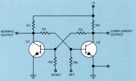
Figure 36. A set-reset flip-flop circuit.
Let's suppose that when the flip-flop is first turned on, Q1 saturates. The collector voltage will drop to zero, so the voltage on the base of Q2 will be zero. Q2 will be cut off, so its collector voltage will be + V. Under these circumstances, the output at the normal out put will be zero, which represents binary O. Suppose, however, that we want it to represent binary 1. We can accomplish this by feeding a positive pulse into the set input.
This will cause Q2 to conduct and go into saturation, so the collector voltage of Q2 will drop practically to zero. When this happens, the base voltage of Q1 will drop to zero so that Q1 will be cut off. With Q1 cut off and its collector current zero, there will be little or no voltage drop across R1. Thus the current swings to + V, so we have a binary 1 stored at the normal output.
If we want to reset the flip-flop to store a binary 0 at the output of Q1, we feed a positive pulse into the reset terminal. This causes Q1 to conduct and saturate, so the voltage at the collector of Q1 drops to zero.
Once again, this causes the base voltage of Q2 to drop to zero so that Q2 will be cut off and the collector voltage will swing to a high positive value. Since the base of Q1 connects to the collector of Q2 through R3, the base of Q1 will be held at a high positive voltage, so Q1 will remain saturated.
This type of flip-flop is called a set-reset flip-flop. Often you will see it referred to as an SR or RS flip-flop. This circuit is also called a latch because the circuit latches in one of the stable states and remains there until changed by a signal fed into the set or reset inputs. The circuit latches itself in either of the two stable states: one where Q1 is cut off, representing a binary 1, and the other where Q2 is cut off and Q1 is saturated, representing a binary 0. Common ICs There are a couple of terms you will see used with ICs and you should know what they mean. One is SSI; this means small scale integration. This is an IC with the equivalent of less than ten gates. MS/ means medium-scale integration. This is an IC with the equivalent of more than ten gates, but less than one hundred. LSI means large-scale integration. This is an IC with the equivalent of more than one hundred but less than a thousand gates. VLSI means very large-scale integration. This is an IC with the equivalent of more than one thousand gates.
Summary
Linear circuits are used to amplify signals so that the output is an amplified version of the input. Digital circuits have only two conditions, on and off.
In digital circuits you are dealing with two logic levels, one of which can be called 1 and the other 0. If logic level 1 is more positive than logic level 0, we have positive logic. If logic level 1 is more negative than logic level 0, we have negative logic. Remember that an inverter is a logic circuit that inverts the logic level.
An AND gate is a gate with two or more inputs that will produce a logic level 1 in the output only when all the inputs are a logic level 1. A NAND gate is an AND gate followed by an inverter.
If you have a logic level 0 on any input of a NAND gate, you'll have a logic level 1 at the output.
An OR gate is a gate that will produce a logic level 1 at the output if there is a logic level 1 on any input. A NOR gate is an OR gate followed by an inverter. A NOR gate will produce a logic level 0 in the output if you have a logic level 1 on any input.
A flip-flop is a circuit with two stable states. It will remain in one of the two stable states until some external signal causes it to flip to the other stable state.
Self-Test Questions
17. How will a series of positive pulses fed into the input of an inverter appear at the output?
18. What is the name given to the gate where a binary 1 must be present at both inputs in order to produce a binary 1 in the output?
19. What is the name given to a gate where a binary 1 at either input will produce a binary 1 at the out put?
20. If there is a binary 1 at one input of a NAND gate, will there be a binary 1 in the output?
21. If a binary 1 is fed into one input of a NOR gate, will there be a binary 1 in the output?
22. If the flip-flop circuit shown in Fig. 36 is storing a binary 0 in the normal output, how do we change it to store a binary 1?
23. If we feed a binary 1 signal to two inputs of a 4-input AND gate, will we get a binary 1 in the output?
ANSWERS TO SELF-TEST QUESTIONS
1. Reverse biased. Zener diodes pass very little current until the break down voltage is reached. This is the voltage that the zener maintains constant. Once this voltage is reached, if the voltage across the diode tends to increase, the current will increase rapidly to maintain the voltage constant.
2. 3 volts. If the voltage drop across each diode is 0.6 volt, and five are connected in series, the voltage across the five will be 5 x 0.6 = 3.0 volts.
3. The diodes are likely to have identical characteristics because they will all be formed at the same time in the manufacturing of the IC. Since they will be formed under identical conditions, it is likely that they will have identical characteristics.
4. Zero. If a 1 volt positive signal is applied to each input, it will cause the current through each transistor to increase, which will cause identical voltage drops across R2 and R3 so that the voltage between E1 and E2 will be zero.
5. In phase. The positive-going signal applied to the input of Q1 will cause the collector current to increase.
This will cause the current through R2 to increase, which will swing the emitter of Q2 in a positive direction. This will reduce the forward bias across the emitter-base junction so that the current through the transistor and through R3 will decrease. If the current through R3 decreases, the voltage drop across it will decrease so that the voltage between the collector and ground will increase.
6. It is a constant-current source. Q3 is also called a current sink. If the current through Q1 increases, the current through Q2 will decrease because the current through Q3 remains constant.
7. Q3 is an emitter-follower. It is used to isolate the differential amplifier made up of Q1 , Q2, and the following stage. It is also used to re duce the DC output voltage so that the output can be fed to another differential amplifier. By connecting differential amplifiers followed by an emitter-follower in this way, we can build an amplifier with a very good low-frequency response; as a matter of fact, it will even respond to de at the input.
8. It has a higher gain and a higher input impedance.
9. A compound-connected differential amplifier will have a much higher gain.
10. Q3 and Q6.
11. Two differential amplifiers, each with a current sink.
12 The circuit shown in Fig.18 has a single-ended input. The input is fed into terminal 7.
13. We have a push-pull output. By looking at Fig.18, you see that the output is taken from terminals 11 and 12. By referring to Fig.19, you see that terminal 11 is the collector of one transistor and terminal 12 is the collector of the other transistor in a differential amplifier.
14. Less than one-half inch. Figure 20 shows that the maximum diameter of the transistor is 0.370 inch, or considerably less than one-half inch.
15. To identify the various pins of a TO-116 case, you hold the IC with its top toward you and the index point on the left. The first pin on the lower left is pin 1. The lower pins are numbered 1 through 7. The 22 upper pins are numbered from the right, pin 8 through pin 14.
16. In a 24 lead, dual in-line package, the pin at the same end as and opposite pin 1 will be pin 24.
17. They will appear as a series of negative-going pulses. The inverter inverts the input signal.
18. An AND gate.
19. An OR gate. 23 20 Yes. A NAND gate is made up of an AND gate and an inverter. If a logic level 1 is fed to one input of the AND gate, the output will be logic level 0. The inverter will invert this so that binary 1 will appear in the output.
No. A NOR gate is made up of an OR gate and an inverter. If a binary 1 is fed into one input of an OR gate, a binary 1 will appear in the output. The inverter will invert this so that the output will be a binary 0. We feed a positive pulse into the set terminal. This will cause Q2 to conduct so that the voltage between the collector and ground of Q2 will drop practically to zero. This will cause the base voltage of Q1 to drop to zero, so that Q1 will cut off and the collector voltage on Q1 will swing to the + V level, which is the logic 1 or binary 1 level.
No. In a 4-input AND gate, we must have a logic level 1 at all four in puts before we'll get a logic level 1 in the output.
LESSON QUESTIONS
This is Lesson Number 2228.
Make sure you print your name, student number, and lesson number in the spaces provided on the Lesson Answer Form. Be sure to fill in the circles beneath your student number and les son number.
Reminder: A properly completed Lesson Answer Form allows us to evaluate your answers and speed the results and additional study material to you as soon as possible. Do not hold your Lesson Answer Forms to send several at one time. You may run out of study material if you do not send your answers for evaluation promptly.
1. In the circuit shown in Fig.11, if a positive-going signal is fed to input 1 and a negative-going signal is fed to input 2, the current flow will increase through:
a. R1.
b. R2.
c. R3.
d. R4.
2. If in-phase sine wave signals, each having an amplitude of 1 volt, are fed to inputs 1 and 2 of the differential amplifier shown in Fig.11, the output between the two output terminals will be:
a. 0 volts.
b. 1 volt.
c. 2 volts.
d. 4 volts.
3. If an input signal swings the base of Q1 in Fig.12 positive, which of the following statements is true?
a. The collector of Q1 will swing negative.
b. The collector of Q2 will swing positive.
c. The base of Q2 will swing positive.
d. The emitter of Q2 will swing negative.
4. One of the important characteristics of the compound-connected emitter follower circuit is:
a. High output impedance.
b. High input impedance.
c. Low input impedance.
d. None of the above.
5. In the compound-connected differential amplifier shown in Fig.16, which two transistors have the highest collector current?
a. Q1 and Q2.
b. Q3 and Q4.
c. Q1 and Q3.
d. Q2 and Q4.
6. In the IC shown in Fig.17, Q3 is:
a. A current source.
b. Part of a Darlington circuit.
c. A voltage regulator.
d. None of the above.
7. In a 4-input AND gate, in order to have a logic level 1 in the output, we must have a logic level 1 at:
a. One input.
b. Two inputs.
c. Three inputs.
d. Four inputs.
8. In order to get a logic level 1 in the out put of a 2-input OR gate, you need a logic level 1 at:
a. Input A.
b. Input B.
c. Inputs A and B.
d. All three of the above will produce a 1 in the output.
9. You will have a logic level 0 in the out put of a 2-input NAND gate when you have:
a. Logic 1 at both inputs.
b. Logic 0 at both inputs.
c. Logic 1 at input A.
d. Logic 1 at input B.
10. If a logic level 1 is stored in the normal output of the set-reset flip-flop shown in Fig.36:
a. Q1 will be cut off.
b. Q2 will be cut off.
c. Q1 and Q2 will be cut off.
d. Q1 and Q2 will be saturated.
------------------
WISHERS AND DOERS
How often have you said "I wish I had more money"? Many times, possibly. But do you realize that if you are living in a town with a population of 5,000, there may be 4,999 other people saying exactly the same thing! And yet, of these 5,000 "wishers," only about 100 are going to do something about it. The others are going to continue dreaming.
Now, any person who shows enough self-motivation to undertake this course proves that he or she is not a mere wisher. Your job now is to keep going forward on the road you have mapped out for yourself.
Every lesson in this course and every goal you work toward is a step along the road. Don't let yourself wish that the lessons were easier, that you could become successful without effort, or that well-paying jobs would come looking for you. Do something to make your dreams a reality. Stay out of the class of the "wisher" - stay in the class of the "doer."
--------------------------