AMAZON multi-meters discounts AMAZON oscilloscope discounts
Amplitude Modulation
In amplitude modulation (AM), the height or amplitude of the carrier is determined by the modulating waveform. Figure 1-16A shows the origin al sine wave carrier with constant amplitude. Figure 1-16B is the modulating waveform. Figure 1-16C is the modulated carrier with the modulating waveform determining the amplitude of the carrier. The modulating waveform can be seen as the envelope of the modulated waveform. When the modulating waveform increases, the amplitude of the carrier increases. When the modulating waveform decreases, the amplitude of the carrier decreases.
Frequency Modulation
Frequency modulation (FM) also modulates a sine wave carrier, but the amplitude of the carrier remains constant while the frequency of the carrier changes. When the modulating waveform increases, the carrier frequency (the number of cycles per second) increases. When the modulating waveform decreases, the instantaneous carrier frequency de creases. A frequency modulated signal is shown in Figure 1-16D.
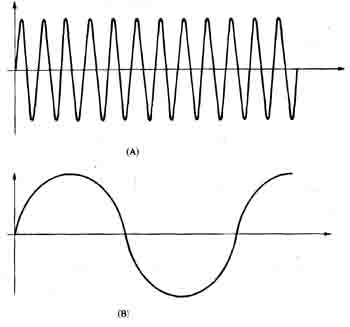
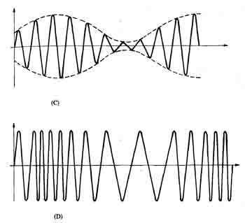
Figure 1-16. Amplitude and frequency modulation. (A) The original
carrier. (B) The modulating signal. (C) The resulting signal if amplitude
modulation is used. (D) The resulting signal if frequency modulation
is used.
Phase modulation is very similar to frequency modulation. The carrier amplitude remains constant and the phase is changed according to the modulating waveform. Since phase and frequency are closely related for our purposes, the effect of phase modulation is very similar to frequency modulation. In fact, phase and frequency modulation may be indistinguishable in a practical measurement system. They are generally considered to be variants of a type of modulation called angle modulation.
Both AM and FM are used in a wide variety of communication systems, including standard radio broadcast stations. The radio station takes its modulating waveform (the data, voice, or music to be broadcast) and superimposes it onto the radio frequency carrier using either AM or FM. At the receiving end, the listener’s radio receiver extracts the modulation from the incoming signal to recover the desired data, voice, or music information.
Modulating a carrier, either with AM or FM, has an effect in the frequency domain (Figure 1-17). With no modulation, the carrier is just a pure sine wave and exists only at one frequency (Figure 1-17A). When the modulation is added, the carrier is accompanied by a band of other frequencies, called sidebands. The exact behavior of these sidebands depends on the level and type of modulation, but in general the side bands spread out on one or both sides of the carrier (Figure 1-17B). Often they are relatively close to the carrier frequency, but in some cases such as wideband FM, the sidebands will spread out much farther. In all cases, modulation has the effect of spreading the signal out in the frequency domain, occupying a wider frequency space.
When a carrier is amplitude modulated by a single sine wave with frequency fM, two modulation sidebands appear (offset by fM) on both sides of the carrier (Figure 1-17C). Carriers that are frequency modulated may have a considerably larger number of sidebands. With a modulating frequency of fM, the sidebands appear at integer multiples of fM away from the carrier frequency. In the general case, FM is a wideband form of modulation, in that the modulated carrier has sidebands that extend out farther than fM away from the carrier. If the modulation occurs at a low level, FM may be narrowband, with sidebands very similar to the AM case. For both modulation schemes, when the modulating signal is complex (voice waveforms, multiple sine waves, etc.) the sidebands will also be more complex.
Radio systems represent intentional use of modulation. Sometimes modulation is produced due to imperfections in practical circuits. In this case, the modulation is either undesirable or at least unnecessary. The effect in the frequency domain is still the same, however, so a sine wave with some residual modulation on it will have sidebands on it in the frequency domain, causing the signal to spread out. This may be an important consideration in an electronic system.
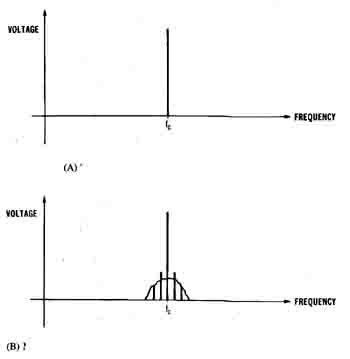
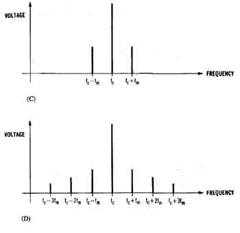
Figure 1-17. The effect of modulation in the frequency domain
is to spread out the signal by creating sidebands. (A) The unmodulated
carrier is a single spectral line. (B) Modulation on the carrier
spreads the signal out in the frequency domain. (C) An AM carrier
(with single sine wave modulation) has a single pair of sidebands.
(D) An FM carrier (with single sine wave modulation) may have many
pairs of sidebands.
Digital Signals
With the widespread use of microprocessor and other digital systems, digital signals have become very common. The basic advantage (and simplicity) of a digital signal is that it has only two valid states: high and low (Figure 1-18). The high state is defined as any voltage greater than or equal to VH and the low state is defined as any voltage less than or equal to YL. Any voltage between VH and VL is undefined. VH and VL are called the logic thresholds.
A typical, well-behaved digital signal (a pulse train) is shown in Figure l-19A. Whenever the voltage is VO.P, the digital signal is interpreted as a high. Whenever the voltage is zero, the digital signal is low. The digital signal in Figure 1-19B is not so well behaved. The signal starts out low, then enters the undefined region (greater than YL but smaller than VH), then becomes high, then low and high once more.
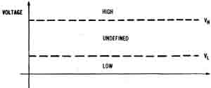
Figure 1-18. A digital signal must be one of two valid states,
high or low.
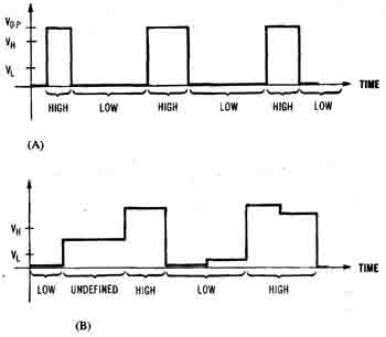
Figure 1-19. Two digital signals. (A) A well behaved digital signal
which is always a valid logic level. (B) A digital signal that's undefined at one point.
Notice that in the last low state, the voltage is not zero but increases a small amount. It does stay less than VL, so it's still a low signal. Similarly, during the last high state the voltage steps down a small amount, but stays above the high threshold.
Although the region between the two logic thresholds is undefined, it does not follow that it should never occur. First of all, to get from a low to a high, the waveform must pass through the undefined area. Also, there are times when one digital gate goes into an “off” or high impedance state while another gate drives the voltage high or low. During this transition, the voltage could stay in the undefined area for a period of time. It is imperative that the digital signal settle to a valid logic level before the digital circuit following it uses the information. Otherwise, a logic error may occur.
Digital signals are mostly used to represent the binary numbers 0 and 1. If positive logic is being used, then a high state corresponds to a logical 1 and a low state corresponds to a logical 0. Although positive logic may appear to be the most obvious convention, negative logic is also sometimes used. With negative logic, the high state represents a logical 0, and the low state represents a logical 1. Thus, the relationship between the voltage of the digital signal and the binary number which it represents varies depending on the logic convention used. Fortunately, the concepts associated with digital signals remain the same, but the instrument user may be left with a digital bookkeeping problem.
Logic Families
There are several different technologies used to implement digital logic circuits. In general, they have unique values for the logic thresholds (VH, VL). In order to interpret a digital signal from a given logic technology or family, these thresholds must be known. Table 1-2 lists logic thresholds for the most popular logic families. All values are in volts. The values may vary slightly with different types of parts within the same general family.
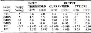
Table 1-2. Logic Thresholds for the Most Common Digital Logic
Families
The logic thresholds are different depending on whether you are concerned with the input of a gate or the output of a gate. The VL for the output of a gate is lower than the VL for the input to a gate. Similarly, the VH for the output is higher than V for the input. This slight amount of intentional over-design guarantees that the output of a digital circuit will drive the input of the next circuit well past its required logic threshold. The difference between the input threshold and the out put threshold is called the noise margin, since the excess voltage is designed to overcome any electrical noise in the system. In general digital testing, the measurement instrumentation should usually be considered a digital input and the logic levels associated with the input should be used.
Decibels
The decibel (dB) is sometimes used to express electrical quantities in a convenient form. The definition of the decibel is based on the ratio of two power levels (log indicates the base ten logarithm):
dB = 10 log (P2/P1)
Since P = V^2 / R (assuming RMS voltage),
dB = 10 log ((V2^2 )/ (V1^2/R1))
and if Ri1= R2 (the resistances involved are the same)
dB = 10 log (V2/V1)^2
dB = 20 log (V2/V1)^2
Voltages V1 and V2 are normally RMS voltages. If the two wave forms are the same shape (for instance, if they are both sine waves), the voltages can be expressed as zero to peak or peak to peak. Since many of our measurements are voltage measurements, calculating decibels using voltages is the most convenient method. Strictly speaking, the voltage equation is valid only if the two resistances involved are the same. For instance, if the input voltage and output voltage if an amplifier were being compared and the input resistance and output resistance are different, they must be accounted for when calculating decibels. In practice, however, this is often ignored. For instance, in operational amplifier circuits, the input impedance is very large while the output impedance is quite small. Usually, the important parameter in this type of circuit is voltage gain (and not power gain). In this type of system, the decibel equation for voltage is used almost exclusively.
To convert decibel values back into a voltage or power ratio, a little reverse math is required:
P2/P1= 10(dB/10)
V2/V1= 10(dB/20)
The usefulness of decibels is sometimes questioned but they are widely used and must be understood by instrument users for that reason alone. In addition, they have at least two characteristics which make them very convenient:
1. Decibels compress widely varying electrical values onto a more manageable logarithmic scale. The range of powers extending from 100 watts down to 1 microwatt is a ratio of 10,000,000 but is expressed in decibels as only 80 dB.
2. Gains and losses through circuits such as attenuators, amplifiers, filters, etc. when expressed in decibels can be added together to produce the total gain or loss. To perform the equivalent operation without decibels requires multiplication.
Some cardinal decibel values are worth pointing out specifically: 0 dB corresponds to a ratio of 1 (for both voltage and power). A circuit that has 0 dB gain or 0 dB loss has an output equal to the input.
3 dB corresponds to a power ratio of 2. A power level that's changed by -3 dB is reduced to half the original power. A power level that's changed by +3 dB is doubled.
6 dB corresponds to a voltage ratio of 2. A voltage that's changed by -6 dB is reduced to half the original voltage. A voltage that's changed by +6 dB is doubled.
10 dB corresponds to a power ratio of 10. This is the only point where the decibel value and the ratio value are the same (for power).
Absolute Decibel Values
Besides being useful for expressing ratios of powers or voltages, decibels can be used for specifying absolute voltages or powers. Either a power reference or voltage reference must be specified. For power calculations:
dB (absolute) = 10 log (P/Pref)
and for voltage calculations:
dB (absolute) = 20 log (V/Vref)
dBm
A convenient and often used power reference for instrumentation use is the milliwatt (1 mW or 0.001 watt), which results in dBm:
dBm = 10 log (P/0.001)
This expression is valid for any impedance or resistance value. As long as the impedance is known and specified, dBm can be computed using voltage. For a 50-ohm resistance, 1 mW of power corresponds to a voltage of 0.223 volt RMS:
P = Vrms^2 / R
Vrms = √PR< = √ (0.001 x 50) = 0.223 volt RMS
Using this voltage as the reference value in the decibel equation results in:
dBm (50 ohm) = 20 log (Vrms / 0.223)
Similarly, for 600 ohms and 75 ohms:
dBm (600 ohm) = 20 log (Vrms / 0.775)
dBm (75 ohm) = 20 log (Vrms / 0.274)
These equations are valid only for the specified impedance or resistance.
dBV
Another natural reference to use in measurements is one volt. This results in the following:
dBV = 20 log (V/ 1)
or simply
dBV = 20 log (V)
This equation is valid for any impedance level (since it’s reference is a voltage). Chart 1-3 summarizes these equations, and Figures 1-20 and 1-21 are plots of the basic decibel relationships. Table 1-3 is a table of voltage and power ratios along with their decibel values. The reader is encouraged to spend some time studying these figures to get a feel for how decibels work.
Chart 1-3.: Summary of Equations Relating to Decibel Calculations. Voltages Are RMS values
dB dB dBm dBV dBm (50 ohm) dBm (75 ohm) dBm (600 ohm) |
= 10log (P2 / P1) = 20 log (V2 / V1) = 20 log P/0.001) = 20 log (V) = 20 log (V / 0.223) = 20 log (V / 0.274) = 20 log (V / 0.775) |
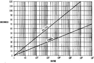
Figure 1-20. Graph for converting ratios to and from decibels
for both voltage and power. Because of the logarithmic relationships,
the plots are straight lines on log axes.
EXAMPLE 1-6. A 0.5-volt RMS voltage is across a 50-ohm resistor. Express this value in dBV and dBm. What would the values be if the resistor were 75 ohms?
50 ohm case:
dBV = 20 log (0.5) = -6.02 dBV
dBm (50 ohm) = 20 log (0.5/0.223) = + 7.01 dBm
75 ohm case:
dBV is based on voltage so that value is the same as the 50 ohm case (-6.02 dBV).
dBm is referenced to 1 mW of power. We must either use the voltage equation for dBm (75 ohm) or compute the power and use the power equation. We will compute the power.
P = Vrms^2 = (05)^2 / 75 = 3.33 mW
dBm = 10 log (P/0.001) = 10 log (0.00333/0.001)
dBm = 5.23 dBm
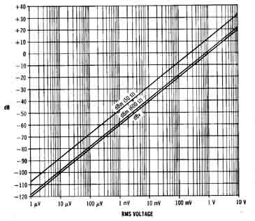
Figure 1-21. Graph of decibels vs. voltage for dBV, dBm (50 ohm) and dBm (600 ohm).
Other References
Other power reference values are 1 watt (dBW) and 1 femtowatt or 1 X 10^-15 watt (dBf). These values can be computed by the following equations:
dBW = 10 log (P)
dBf = 10 log (P/ (1 X 10^-15))
Voltage or power measurements relative to a fixed signal (called the carrier) are expressed as dBc.
dBc = 10 log (P/Pcarrier)
or
dBc = 20 log (V/Vcarrier)
The reader will undoubtedly encounter other variations. The number of possible permutations on the lowly decibel is limited only by the imagination of engineers and technicians worldwide. (It is rumored that some electrical engineers balance their checkbooks using dB$.)
Measurement Error
Because imperfections in any measuring instrument will disturb the circuit being tested by removing energy from that circuit (no matter how small), some amount of error will always be introduced. Another way of saying this is that connecting an instrument to a circuit changes that circuit and changes the voltage or current that's being measured. This error can be minimized by careful attention to the loading effect as discussed later.
Internal Error
In addition, errors internal to the instrument degrade the quality of the measurement. These errors fall into two main categories:
ACCURACY: the ability of the instrument to measure the true value to within some stated error specification.
RESOLUTION: the smallest change in value that an instrument can detect.
Suppose a voltage measuring instrument has an accuracy of ±1% of the measured voltage and 3-digit resolution. If the measured voltage was 5 volts, then the accuracy of the instrument (in volts) is 1% of 5 volts or ± 0.05 volt. The instrument could read anywhere from 4.95 to 5.05 volts with a resolution of 3 digits. The meter can't , for instance, read 5.001 volts since that would require 4 digits of resolution.
If the instrument had 4-digit resolution (but 1% accuracy) then the reading could be anywhere from 4.950 to 5.050 volts (the same basic accuracy, but with more digits). Assume for the moment that both meters read exactly 5 volts. If the actual voltage changed to 5.001 volts, the 3-digit instrument would probably not register any change, but the 4-digit instrument would have enough resolving power to show that the voltage had indeed changed. (Actually, the 3-digit meter reading might change, but could not display 5.001 volts because the next highest possible reading is 5.01 volts.) The accuracy of the 4-digit instrument is not any better, but it has finer resolution so it measures smaller changes. Neither meter guarantees that a voltage of 5.001 volts can be measured any more accurately than 1%.
The example given is a digital instrument, but the same concepts apply to analog instruments. Resolution is not usually specified in digits in the analog case, but all instruments have some fundamental limitation to their measurement resolution. Typically, the limitation is the physical size of the analog meter and its markings. For instance, an analog volt meter with full scale equal to 10 volts will have difficulty detecting the difference between two voltages which differ by a few microvolts. Usually, an instrument provides more measurement resolution than measurement accuracy. This guarantees that the resolution will not limit the obtainable accuracy and allows detection of small changes in readings (even if those readings have some absolute error in them). The relative accuracy between small steps may be much better than the full-scale absolute accuracy.
The Loading Effect
In general, when two circuits are connected together the voltages and currents in those circuits both change. One circuit is referred to as the source and the other circuit as the load. The source might be, for example, the output of an amplifier, transmitter, or signal generator. The corresponding load might be a speaker, antenna, or the input of a circuit. In the case where an electronic measurement is being made, the circuit under test is the source and the measuring instrument is the load. The measuring instrument always has an effect on the circuit, but if this loading effect is small enough, it can be ignored.
Many source circuits can be represented by a voltage source, V and a series resistance, R (Figure 1-22). Thus, complex circuits can be simplified by replacing them with an equivalent circuit model. In the same way, many loads can be replaced conceptually with a circuit model consisting of a single resistance, RL. (Resistive circuits will be considered initially in this discussion, but later expanded to include AC impedances.)
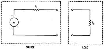
Figure 1-22. A voltage source with internal resistance and a resistive
load.
Vs is also known as the open circuit voltage, since it's the voltage across the source circuit with no load connected. This is easily proven by noting that no current can flow through Rs under open circuit conditions. Therefore, there is no voltage drop across Rs (V = IR), and VL = Vs.
The Voltage Divider
When the load is connected to the source, the voltage across the source (and the load), VL, is no longer the open circuit value, V VL is given by the voltage divider equation (named for the manner in which the total voltage in the circuit divides across R and RL).
VL = Vs RL/(Rs + RL)
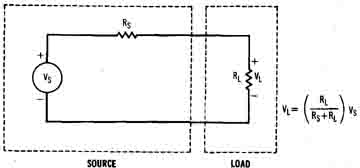
Figure 1-23. The source and load are connected together. The voltage
across the load is given by the voltage divider equation.
Figure 1-23 shows a source and load connected in this manner. The resulting output voltage, VL, as a function of the ratio R is plotted in Figure 1-24. If RL is very small compared to R then VL is also very small. For large values of RL (compared to Rs) VL approaches Vs.
Maximum Voltage Transfer
To get the maximum voltage out of a voltage source being loaded by some resistance, it's necessary to make the ratio RL/Rs as large as possible. From a design point of view, this can be approached from two directions: make R small or make RL large. Ideally, we could make Rs = 0 and make RL = infinity, resulting in VL = Vs. In practice, this can't be obtained, but can be approximated. Figure 1-24 shows that making RL ten times larger than R results in a voltage that's 91% of the maximum attainable (Vs) The larger the load resistance, the better the voltage transfer.
When making measurements, the source is the circuit under test and the load is the measuring instrument. We may not have control over the value of R (if it's part of the circuit under test) and our only recourse is choosing RL (the resistance in our measuring instrument). Ideally, we would want the resistance of the instrument to be infinite, causing no loading effect. In reality, we will settle for an instrument which has an equivalent load resistance that's much larger than the equivalent resistance of the circuit.
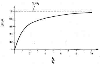
Figure 1-24. A plot of the output voltage due to the loading effect,
as a function of the load resistance divided by the source resistance.
Maximum Power Transfer
Sometimes the power delivered to the load resistor is more important than the voltage. Since power depends on both voltage and current (P = VI), maximum voltage does not guarantee maximum power. The power delivered to RL can be determined as follows:
P = VI
P = Vs/RL / (RL + Rs) x Vs/(RL + Rs)
P = Vs^2 RL/(RL + Rs)^2
This relationship is plotted for varying values of RL/Rs in Figure 1-25. For small values of RL (relative to R the power delivered to RL is small, because the voltage across RL is small, large values of RL (relative to R the power delivered is also small because the current through RL is small. The power transferred is maximum when RL/Rs = 1 or, equivalently, when RL equals Rs.
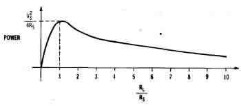
Figure 1-25. Plot of output power as a function of the load resistance
divided by the source resistance.
In many electronic systems, maximum power transfer is desirable. Such systems are designed with all source resistances and load resistances being equal to maximize the power. Maximum power transfer is achieved while sacrificing maximum voltage transfer between the source and load. Maximum power and maximum voltage don't necessarily occur for the same load resistance because power depends on both voltage and current.
Impedance: So far, the discussion of loading has assumed resistive circuits. Now lets define the concept of impedance (Z).
where
Z = Vac / Iac
Vac is the AC voltage across the impedance, Vac is the AC current through the impedance.
Since impedance is the ratio of a sine-wave voltage to a sine-wave current, it's similar to the concept of resistance, except that it's valid only for sine waves. But it's only similar to, not the same as resistance, since the value of the impedance may be different for each frequency (ideally, resistors are constant with frequency). Also, a phase angle may be associated with a given impedance because the voltage and current are not necessarily in phase. The magnitude and phase of the impedance may be accounted for by the use of complex numbers or by stating the magnitude and phase explicitly in magnitude and phase format. Impedances are commonly expressed as complex numbers:
Z = R + jX
where:
In magnitude/phase format:
Z=ZM angle theta
For the purposes of maximum power transfer, when the source impedance and load impedance are not resistive, maximum power transfer occurs when the load impedance has the same magnitude as the source impedance, but with opposite phase angle. For instance, if the source impedance was 50 ohms with an angle of +45 degrees, the load impedance should be 50 ohms with an angle of -45 degrees to maximize the power transfer. A special case is when the phase angle of the source impedance is zero. In that case, the load impedance should have the same magnitude as the source impedance and an angle of zero (load impedance equals source impedance). Note that this is the same as in the purely resistive case.
Instrument Inputs
The characteristics of instrument input impedances vary quite a bit among individual models, but in general they can be put into two categories: high impedance and system impedance.
High-Impedance Inputs
High-impedance inputs are designed to maximize the voltage transfer from the circuit under test to the measuring instrument by minimizing the loading effect. As outlined previously, this can be done by making the input impedance of the instrument much larger than the impedance of the circuit. Typical values for instrument input impedance are between 10 k-Ohm and 1 M-Ohm. For instruments used at high frequencies, the capacitance across the input becomes important and , therefore, is usually specified by the manufacturer.
System-Impedance Inputs
Many electronic systems have a particular system impedance such as 50 ohms (Figure 1-26). If all inputs, outputs, cables and loads in the system have the same impedance then, according to the previous discussion, maximum power is always transferred. At high frequencies (above 30 MHz), stray capacitance and transmission line effects make this the only type of system that's practical. The system impedance is often called the characteristic impedance and is represented by the symbol Z0.
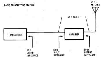
Figure 1-26. An electronic system that uses a common system impedance
for maximum power transfer throughout.
At audio frequencies, a constant system impedance is not mandatory but is often used. It is sufficient for many applications to make all source circuits have a low impedance (less than 100 ohms) and all load circuits have a high impedance (greater than 1000 ohms). This results in near maximum voltage transfer (power transfer is less important here). Some audio systems do maintain, or at least specify for test purposes, a system impedance which is 600 ohms. This same impedance shows up in telephone applications as well.
For radio frequency work, 50 ohms is by far the most common impedance. This impedance can be easily maintained despite stray capacitance and 50 ohm cable is easily realizable. Such things as amateur and commercial radio transmitters, transmitting antennas, communications filters, and radio frequency test equipment all commonly have 50- ohm input and output impedances. Runner-up to 50 ohms in the radio frequency world is 75 ohms. This impedance is also used extensively at these frequencies, particularly in video-related applications such as cable TV. Other system impedances are used as special needs arise and will be encountered when making electronic measurements.
When measuring this type of system, most of the accessible points in the system expect to be loaded by the system impedance (Z Because of this, many instruments are supplied with standard input-impedance values (again, typically 50 ohms). Thus, the instrument can be connected into the system and act as a 50-ohm load while it's measuring. This technique keeps the measured values consistent with normal system operation.
Bandwidth
Instruments that measure AC waveforms generally have some maximum frequency above which the measurement accuracy is degraded. This frequency is the bandwidth of the instrument and is usually defined as the frequency at which the instrument’s response has decreased by 3 dB. (Other values such as 1 dB and 6 dB are also sometimes used.) A typical response is shown in Figure 1-27. Note that the response does not instantly stop at the 3-dB bandwidth. It begins sluggishly decreasing at frequencies less than the bandwidth, and the response is still fairly large for frequencies outside the bandwidth. Some instruments will have their bandwidth implied in their accuracy specification. Rather than give a specific 3-dB bandwidth, the accuracy specification will be given as valid only over a specified frequency range.
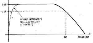
Figure 1-27. The frequency response of a typical measuring instrument
rolls off at high frequencies.
In general, to measure an AC waveform the instrument must have a bandwidth that exceeds the frequency content of the waveform. For a sine wave, the instrument bandwidth must be at least as large as the sine-wave frequency. For sine-wave frequencies equal to the 3-dB band width, the measured value will, of course, be decreased by 3 dB, so an even wider bandwidth is desirable. The amount of margin necessary will vary depending on how slowly the response rolls off near the 3-dB point and the measurement accuracy desired.
For sine-wave measurements, the frequency response near the 3-dB bandwidth can be adjusted for by recording the response at these frequencies using a known input signal. Assuming the response is repeatable, the measurement error due to limited bandwidth can be used to adjust the measured value to obtain the actual value.
Instruments that measure only AC voltages (and not DC) will have a response that rolls off at low frequencies as well as high frequencies.. When using instruments of this type (including many AC voltmeters), both high- and low-frequency bandwidth limitations must be considered.
For waveforms other than sine waves, the harmonics must be considered. If the harmonics are outside the instrument bandwidth then their effect on the waveform will not be measured. This could actually be desirable if the harmonics outside some frequency range needed to be ignored, but, in general, their effect is usually desirable in the measurement. Waveforms with an infinite number of harmonics would require an instrument with infinite bandwidth to measure them. In reality, the higher harmonics have very little energy and can be ignored with proper regard to how much error this produces in the measurement.
Rise Time
Ideally, waveforms such as square waves and pulses change voltage level instantaneously. In reality, waveforms take some time to make an abrupt change, depending on the bandwidth of the system and other circuit parameters. The amount of time it takes for a waveform in transition from one voltage to another is called the rise time. (The rise time is normally measured at the 10% and 90% levels of the transition.) The bandwidth of a measuring instrument will limit the measured rise time of a pulse or square wave. For a typical instrument, the relationship between rise time and bandwidth is given by:
t(rise) = 0.35/BW
where
BW = 3-dB bandwidth (in Hz).
The validity of this relationship depends on the exact shape of the frequency response of the instrument (how fast it rolls off for frequencies above its bandwidth). It is exact for instruments that roll off at —20 dB per decade (factor of 10) in frequency above the 3-dB bandwidth and is a good approximation for most instruments. (These types of instruments are said to have a single-pole frequency response.) The important point here is that the bandwidth, which is a frequency domain concept, will limit the measurement of the rise time, which is a time domain concept. The two characteristics of the instrument (time domain and frequency domain) are inextricably intertwined. Fast changes (small rise times) correspond to high-frequency content in a waveform, so if the high- frequency content is limited by the bandwidth of a system then the rise time will be larger.
The instrument should have a rise time significantly smaller than the rise time being measured. A rise-time measurement using an instrument with a rise time two times smaller than the one being measured will result in an error of about 10 percent. This error drops to 1 percent when the instrument rise time is 5 times shorter than the measured rise time.
Bandwidth Limitation on Square Wave
As an example of how limited bandwidth can affect a waveform in the time domain, consider the square wave shown in Figure 1-28. The wave form is passed through a low-pass filter which has a frequency characteristic similar to Figure 1-27. If the bandwidth of the filter is very wide (compared to the fundamental frequency of the waveform), the square wave appears at the output undistorted. If the bandwidth is reduced, some of the harmonics are removed from the waveform. The output still looks like a square wave, but it has some imperfections that would cause a measurement error. For very limited bandwidth, the square wave barely appears at all, and is very rounded due to the lack of high frequency harmonics.
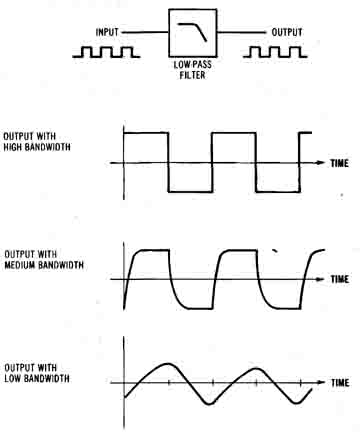
Figure 1-28. The effect of bandwidth on a square wave.
EXAMPLE 1-7. An electronic instrument is used to measure the voltage of a 2-kHz sine wave. What instrument bandwidth is required? What bandwidth would be required to measure a square wave having the same frequency (assume that any harmonic greater than 10% of the fundamental is to be included)?
Since a sine wave has only the fundamental frequency, the bandwidth of the instrument must be at least the frequency of the waveform. BW = 2 kHz. (In reality, we will want to choose a higher value.)
From Table 1-1, the highest significant harmonic (greater than 10% of the fundamental) is the 9th harmonic. Therefore, the band width must be at least (and probably larger than):
BW = 9 x 2kHz=18kHz
EXAMPLE 1-8. A pulse with zero rise time is passed through a low-pass filter with a 3-dB bandwidth of 25 kHz. If the filter has a one-pole rolloff, what will the rise time be at the output?
Even though the rise time at the input is zero, due to the’ 25-kHz bandwidth limitation the rise time at the output will be:
t(rise) = 0.35/ BW = 0.35/ 25 kHz = 14 microseconds
EXAMPLE 1-9. A square wave with a rise time of 1% micro-sec is to be measured by an instrument. What 3-dB bandwidth is required in the measuring instrument to measure the rise time with 1% error?
For a 1% error in rise time, the measuring instrument must have a rise time that's 5 times less than the waveform’s rise time. For the instrument:
t(rise) = 1 µsec / 5 = 0.2 µsec
BW = 0.35/ t(rise) = 0.35 / 0.2 µsec = 1.75 MHz
Table 1-3. Table of Decibel Values for Voltage and Power Ratios
PREV: Measurement TheoryNEXT: Voltmeters, Ammeters, and Ohmmeters