AMAZON multi-meters discounts AMAZON oscilloscope discounts
The oscilloscope produces a picture of the voltage waveform that's being measured. This allows the instrument user to think in terms of the actual waveform when making measurements. Therefore, determining zero-to- peak voltages, RMS voltages, and the like simply means interpreting the scope display using the theory discussed in Section 1. The displayed waveform is subject to the inaccuracies caused by the finite bandwidth of the scope, the loading effect, and errors internal to the scope.
Sine Wave Measurements
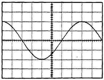
Figure 5-1. Measuring a sine wave voltage using an oscilloscope.
Figure 5-1 shows a typical display of a sine wave using an oscilloscope. The usual sine wave parameters can be determined from the display with a small amount of care. The peak-to-peak voltage can be first found in terms of display divisions and then converted to volts. The peak-to-peak value of the sine wave in Figure 5-1 is 4 divisions. If the vertical sensitivity is set to 0.5 volt per division, then the peak-to-peak voltage is
4 x 0.5 = 2 volts. (This value might need to be adjusted if a divider probe is used. See Section 4.) The zero-to-peak voltage is just 2 divisions, so 2 X 0.5 = 1 volt.
The RMS voltage is not as easy to determine, at least not directly from the oscilloscope. But the relationship between the zero-to-peak and RMS values for a sine wave is known. V = 0.707 Vp-p = (0.707) (1 volt) = 0.707 volt RMS. This calculation is valid only for a sine wave, but conversion factors for other waveforms are included in Section 1. To be precise, the oscilloscope can't measure RMS voltage directly, but does give the user enough information to compute the value for simple waveforms.
The above measurements used the vertical scale to determine voltage information. The horizontal (or time) scale can be used to determine the period of the waveform. The period of the waveform in Figure 5-1 is 8 divisions. With the horizontal axis set at 0.2 msec/div, the period of the signal is (8)(0.2 msec)= 1.6 msec. Although the frequency can't be read from the oscilloscope directly, it can be computed using the period of the waveform.
f = 1/T
The frequency of the waveform in the figure equals 1/1.6 msec or 625 Hz. Frequency is another parameter which can't be determined directly from the oscilloscope, but the scope gives us the information to compute the value.
EXAMPLE 5-1 Determine the zero-to-peak voltage, the peak- to-peak voltage, period and frequency of the waveform shown in Figure 5-2.
The waveform is 1.5 divisions zero-to-peak and 3 divisions peak-to-peak.
Vo-p = 1.5 div X 0.2 volt/div = 0.3 volt
Vp-p = 3 div x 0.2 volt/div = 0.6 volt
The period of the waveform is 3 divisions.
T = 3 div x 500 usec = 1.5 msec.
f = 1/T = 666.67 Hz
Figure 5-2. Oscilloscope waveform for Example 5-1. Vertical sensitivity
= 0.2 volt/division, and time base = 500 usec/division.
Oscilloscope vs. Voltmeter
Figure 5-3 shows a voltmeter and an oscilloscope connected to the output of a function generator. A comparison of the two measurements will highlight the advantages of each. The oscilloscope provides a complete representation of the waveform out of the function generator. Its peak-to- peak and zero-to-peak AC values are easily read and for most waveforms the RMS value can be computed. If there is some DC present along with the waveform, this also will be evident in the voltage vs time display (assuming that the scope is DC coupled). The period and frequency of the waveform can also be measured.
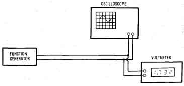
Figure 5-3. The output of a function generator is measured by an
oscilloscope and a voltmeter.
The voltmeter will supply only voltage information about the wave form. Most voltmeters will read RMS, but the accuracy of the reading may be dependent on the type of waveform (if the meter is an average- responding type). Also, no indication is given as to the actual shape of the waveform. The user may assume a given shape, but distortion due to improper circuit operation may cause the waveform to be much different. The voltmeter is easier to use. It requires less interpretation of its dis play, has fewer controls to adjust and its physical size is usually much smaller and more convenient than the scope. Voltmeters are also general ly more accurate for amplitude measurements than oscilloscopes. A typical oscilloscope amplitude accuracy is around 3 percent, while volt meter accuracies are typically better than 1 percent. The voltmeter pro vides no time or frequency information at all.
Voltage Gain Measurement
It is often desirable to measure the gain of circuits such as amplifiers, filters, and attenuators. The voltage gain is defined as
Voltage Gain = G = Vout / Vin
where V and V are the voltages at the input and output of the circuit, respectively (Figure 5-4). In other words, gain describes how big the output is compared to the input. Vin and Vout can be any type of voltage: DC, AC zero-to-peak, AC RMS, etc. as long as both voltages are measured consistently. If the output is larger then the input, the gain is greater than one. If the output equals the input, then the gain is exactly one and if the output is less than the input, the gain is less than one. Circuits with gain less than one can be described as having a loss.
Voltage Loss = Vin / Vout = 1 / G
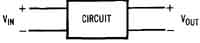
Figure 5-4. The voltage gain of a circuit is determined by dividing
the output voltage by the input voltage.
Gain in Decibels (dB)
Voltage gain can also be expressed in dB:
Voltage Gain (dB) = G = 20 log (V
If the output is greater than the input, the gain (in dB) is a positive number. If the output equals the input, the gain is 0 dB and if the output is less than the input, the gain is negative (in dB). Gain and loss are opposite terms. A gain of -10 dB (output is actually smaller than the input) corresponds to a 10-dB loss.
AC Voltage Gain
Figure 5-5 shows the simplest method for measuring AC voltage gain. A signal source is used to supply the input voltage, and a two-channel oscilloscope is used to measure the input and output voltage of the circuit. The source can be any type capable of producing a sine wave at the frequency of interest. The resulting oscilloscope display is shown in Figure 5-6. The values of the two voltages are determined from the display and the gain is calculated. If the signal level into the circuit is not critical, then it's desirable to set the sine wave source such that the value of Vin is convenient (such as 1 volt) for the gain calculation. Again, the AC voltage can be described in a variety of ways but zero-to peak and peak-to-peak will usually be the most convenient. It is important to maintain proper loading (both input and output) when making voltage gain measurements. Circuits which expect to be loaded with a particular impedance (Z0 systems, for instance) should either be loaded with a resistor or an instrument with the appropriate input impedance. Also, the input to such a circuit should be driven with a source that has the correct output impedance.
EXAMPLE 5-2 Determine the voltage gain for Vin and Vout shown in Figure 5-6. Express the value in dB.
Figure 5-6 shows the zero-to-peak value of V = 1 div X 1 volt/div = 1 volt zero-to-peak, and Vout = 2.5 div X 1 volt/div = 2.5 volts zero-to-peak. The voltage gain, G = Vout / Vin . = 2.5/1 = 2.5. Notice how easy the gain calculation was with Vin equal to 1 volt. In dB, GdB = 20 log 2.5 = 7.96 dB.
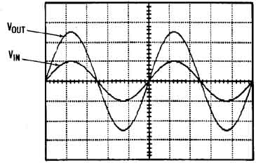
Figure 5-6. The oscilloscope display for measuring the gain of a
circuit. Vertical sensitivity = 1 volt/division.
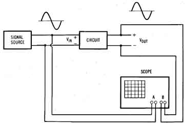
Figure 5-5. Instrument connections for measuring the voltage gain
of a circuit.
Phase Measurement
The waveforms shown in Figure 5-6 have no phase difference between them, but this is not always the case. Many circuits introduce a phase shift between input and output. In some electronic systems, phase shift is unimportant but many times it's a critical parameter to be measured.
Time-Base Method
The same setup shown in Figure 5-5 can be used to measure the phase shift through a circuit. If there is a nonzero phase shift through the circuit, the resulting oscilloscope display will look something like Figure 5-7. (The gain of the circuit is shown as 1 for simplicity.) The scope display gives the user a direct, side-by-side comparison of the two signals and the phase difference can be determined. First, the period of the sine wave is found in terms of graticule divisions. (Recall that one complete cycle corresponds to 360 degrees.) Next, the phase difference is determined in terms of graticule divisions. This can best be done by choosing a convenient spot on one waveform and counting the divisions to the same spot on the other waveform. The starting edge of the sine wave (where it crosses zero) is usually a good reference point since most scope graticules have the middle of the display marked with the finest resolution. The resulting phase difference is:
Phase shift = theta =360 x shift (in div)/period (in div)
The result is in degrees. Since interpreting the oscilloscope display is somewhat tedious, it's recommended that the user double-check the measured value. (This is known as a “reality” check.) This simply means take another look at the display, roughly estimate the phase shift (knowing that one cycle is 360 degrees) and compare this to the calculated answer. The two should be roughly the same.
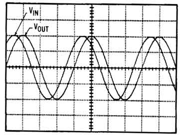
Figure 5-7. The phase difference between two sine waves can be measured
using the time-base method.
The only problem remaining is to determine the sign (positive or negative) of the phase. Vout is normally measured with respect to Vin so Vin is the phase reference. If Vout is shifted to the left of Vin , (Vout leads Vin ), Vout will have a positive phase relative to Vin . If Vout is shifted to the right of Vin (Vout lags Vin ), Vout will have a negative phase relative to Vin . The use of the terms lead and lag are less likely to be confused than calling the phase positive or negative.
Since phase repeats on every cycle (360 degrees), the same phase relationship can be described in numerous ways. For example, if Vin leads Vout by 270 degrees, this will be the same as Vout lagging Vin by 90 degrees. Although both of these expressions are technically correct, it's recommended that phase differences be limited to ±180 degrees. So the appropriate expression would be that Vout lags Vin by 90 degrees.
EXAMPLE 5-3 Determine the phase difference between the V and V as shown in Figure 5-7.
The period of both waveforms is 4 divisions. The phase shift in divisions is 1/2 of a division:
theta = 360 X 0.5 / 4 = 45 degrees
Since Vout is shifted to the right of Vin , Vout lags Vin by 45 degrees or equivalently, Vin leads Vout by 45 degrees.
Lissajous Method
Another method for measuring the phase between two signals is called the Lissajous method (or Lissajous pattern). Although somewhat more complicated, this method will usually result in a more accurate phase measurement. Figure 5-8 shows a scope connected such that the phase between the output and input of a circuit can be measured. The oscilloscope is configured in the X—Y mode with one signal connected to the horizontal input and the other signal connected to the vertical input.
Figure 5-9 shows the elliptical shape that results from this measurement. Two values, A and B, can be read off the display and can then be used to calculate the phase angle. The value A is the distance from the X axis to the point where the ellipse crosses the Y axis, and the value B is the height of the ellipse, also measured from the X axis. It is important that the scope be set up with both the X and Y axes set at the zero volt level. On most scopes this would be accomplished by grounding both inputs and adjusting the dot on the display to be at the center of the screen. Both of the volts/division controls can be adjusted to allow convenient and accurate reading of the values. The two controls don't have to be set the same, since A and B are measured along the same axis.
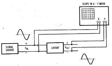
Figure 5-8. The proper connection for measuring the phase difference
between the input and output of a circuit using the Lissajous method.
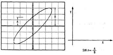
Figure 5-9. The oscilloscope is operated in X—Y mode when using
the Lissajous method.
Two general cases must be considered. If the ellipse runs from lower left to upper right, then the phase angle is between 0 and 90 degrees (Figure 5-10). If the ellipse runs from lower right to upper left, then the angle is between 90 and 180 degrees. The angle can be computed from the A and B values using the appropriate equation as shown in Figure 5-10. Unfortunately, the sign of the angle can't be determined using this method. If the computed answer is 45 degrees, for example, the phase difference may be +45 degrees or -45 degrees. Said another way, the signal on the vertical axis may be leading or lagging the signal on the horizontal axis by 45 degrees. The time-base method can be used to determine the sign, while using the Lissajous method for greater accuracy. A quick look using the time-base method is also a good check on the results from the Lissajous method.
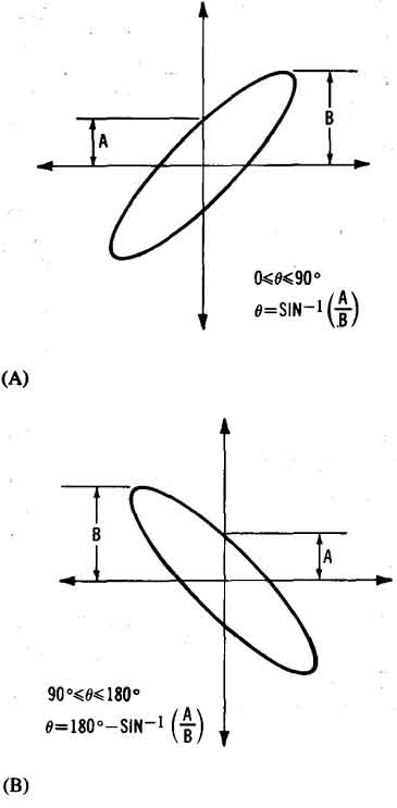
Figure 5-10. The Lissajous method for computing phase has two general cases. (A) The ellipse runs from lower left to upper right. (B) The
ellipse runs from upper left to lower right.
Some special cases of the Lissajous display are shown in Figure 5-11. When the ellipse collapses into a straight line, the two waveforms are in phase. This can be used as a very precise indication when adjusting for zero phase between two signals. If the ellipse is a perfect circle (with both volts/div controls the same), then the waveforms are exactly 90 degrees apart. Again, this could be plus or minus 90 degrees. If the display becomes a straight line, but in the lower right/upper left orientation, then the two signals are exactly out of phase (180 degrees).
EXAMPLE 5-4 Determine the phase difference between the two signals given the Lissajous pattern shown in Figure 5-12.
The ellipse is lower left to upper right. First find the values for A and B. A = 2.3 divisions, B = 3 divisions.
theta = sin^-1( A/B) = sin^-1 ( 2.3/3) = 50 degrees
Note that the vertical sensitivity doesn’t enter into the calculation since A and B are measured on the same axis.
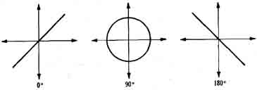
Figure 5-11. Some special cases of the Lissajous phase measurement.
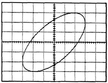
Figure 5-12. Lissajous pattern for Example 5-4.
Lissajous Method for Frequency Measurement
The Lissajous method can also be used to compare the frequency of two sine waves. The oscilloscope, operating in X—Y mode, is connected as shown in Figure 5-13. The frequency being measured is connected to the vertical axis while the reference frequency (hopefully, precisely known) is connected to the horizontal axis. If the two frequencies are the same (have a 1:1 ratio), the situation is exactly the same as the phase measurement case. In A of Figure 5-14, the oscilloscope display is shown for a frequency ratio of 1:1 and a phase shift of 90 degrees. If the phase is other than 90 degrees, then the display will not be a perfect circle, but an ellipse. Again, this case was covered under phase measurement. If the two frequencies are not quite exactly the same then the display will not be stable and the ellipse will contort and rotate on the display.
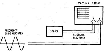
Figure 5-13. The Lissajous method can be used to compare the frequency
being measured with a known reference frequency.
Other frequency ratios are also shown in Figure 5-14. They may also appear warped or slanted in different ways just like the ellipse is a slanted version of a circle (for the 1:1 case). In general, the ratio of the two frequencies is determined by the number of cusps (or humps) on the top and side of the display. Consider B of Figure 5-14. There are 2 cusps across the top and only one cusp along the side, therefore the frequency ratio is 2:1. In D of Figure 5-14, there are 3 cusps across the top and 2 cusps along the side, resulting in a frequency ratio of 3:2. This technique can be applied to any similar frequency ratio. The display will be stable only when the frequency ratio is exact. In general, if the sine waves are not phase locked together, there will be some residual phase drift between the two frequencies with a corresponding movement on the display.
This method of frequency measurement is somewhat limited since it deals only with distinct frequency ratios. It does help if a sine wave source with variable frequency is available for use as the reference. Then the source can be adjusted so that the measured signal’s frequency results in a convenient ratio. Since the method uses frequency ratios, the limiting factor in the accuracy of the measurement is the frequency accuracy and stability of the reference source. If the source used as a frequency reference is not more accurate than the oscilloscope’s time base then there is no advantage in using this method. Instead, the frequency should be computed from the period of the waveform measured in the time-base mode.
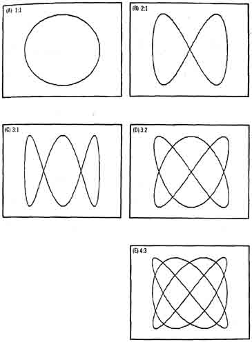
Figure 5-14. Typical Lissajous patterns for a variety of frequency
ratios.
Pulse Measurement
Pulse trains (and square waves) can be measured and characterized using an oscilloscope. The measurement involves connecting the scope to the waveform of interest, obtaining a voltage vs. time display of the wave form, and extracting the parameter of interest from the display. The oscilloscope bandwidth and rise time must be adequate so that the pulse being measured is not corrupted.
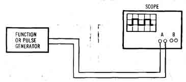
Figure 5-15. The pulse output of a function or pulse generator can
displayed on an oscilloscope.
Various imperfections may exist in a pulse train (Figure 5-16). Be cause of the similarities of the pulse train and square wave, these terms for describing imperfections may also be applied to a square wave. Ideally, the pulse goes from 0 volts to Vo-p in zero time, but due to circuits that can't respond infinitely fast, the rise time is not zero. Rise time is usually specified to be the time it takes to go from 10% of to 90% of Vo-p. Similarly, the fall time is the time it takes for the waveform to go from 90% of Vo-p to 10% of Vo-p. The rise and fall times may or may not be the same.
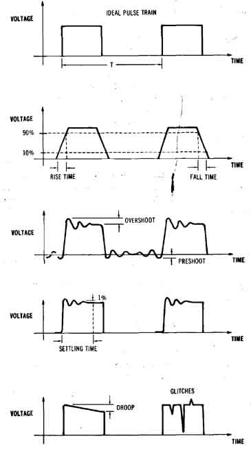
Figure 5-16. The pulse train introduced in Section 1 will usually
have some imperfections in it. The quality of the pulse train can be
determined using an oscilloscope.
The pulse may actually exceed after the rising edge of the pulse and then settle out. The amount that the voltage exceeds is called overshoot, and the time it takes to settle out is called settling time. Settling time is specified such that the waveform has settled to within some small percent of Vo-p (often 1 percent). Pre-shoot is similar to overshoot, except that it occurs before the edge of a pulse.
The top of the pulse may not be perfectly flat, but have some small slope to it. The amount that the top of the pulse slopes down is called droop (or sag). Abrupt voltage changes in the waveform are called glitches and are particularly common in digital circuits. Glitches can be large enough to cause a digital signal to enter the undefined region or in more extreme cases to change logic state. Some circuits will tolerate a certain amount of glitching, but glitches are generally undesirable as they may cause the circuit to malfunction.
Pulse Delay
The time delay between two pulses (for example, in a digital circuit) may be measured using a two-channel scope. Figure 5-17 shows two logic gates (inverters) connected end to end driven by a pulsed logic signal. In all digital technologies it takes a small but nonzero amount of time for the input pulse to reach the output. The oscilloscope is set up to display both the input and output of the two-gate circuit. The resulting time delay between the two waveforms is found by counting the number of divisions between the rising edge of the input pulse and the rising edge of the output pulse. This is then multiplied by the time/division setting on the oscilloscope to obtain the time difference between the pulses.
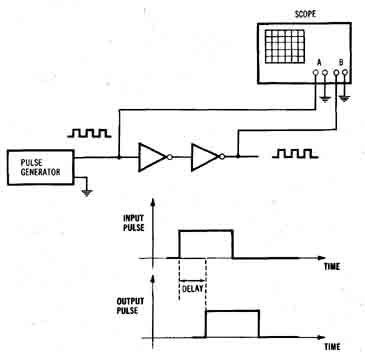
Figure 5-17. An oscilloscope can be used to measure the time delay
between two pulses, as in the input and output of a digital circuit.
Digital Signals
As discussed in Section 1, digital signals can take on one of two valid states: high or low. Assuming positive logic, these two states may be used to represent the binary numbers 1 and 0, respectively. Thus, most digital signals are pulsed in nature. In general, the pulse width and period will depend on the particular digital system. The digital signal may be periodic, repeating the same binary states in a predictable manner, or it may pulse in what appears to be a random manner, with no identifiable repetition. For instance, a digital signal on the data bus of a microprocessor will change according to the data and instructions being read from memory. Usually, there will be no discernible pattern to these binary numbers, and the digital signal will appear to be a sequence of random pulses. (In addition, the data bus may go into the high impedance state between transfers, confusing the situation even further.)
Do not expect to see perfectly clean pulses in digital signals. Even though digital systems are based on the concept of only two valid states, the actual voltage being observed is still an analog voltage capable of having any value within the power supply range. if the output of the driving circuit goes into the high-impedance state, then the voltage may “float” to most any value and will be very susceptible to crosstalk from nearby signals. Also, the digital signal is subject to the same rise time limitations (due to the system bandwidth) as any other signal. Noise can also be a present and , if large enough, can cause a digital signal to change state.
Oscilloscopes tend to show all of the imperfections of the signal. Sometimes this is unnecessary information that can be ignored, but in many cases can be critical to understanding the circuit operation or mal function. A logic analyzer is a better choice for viewing digital signals when the analog characteristics of the signal are known to be good. Logic analyzers have the advantage of handling large numbers of signals efficiently as well as providing very versatile trace capability. But for critical timing or signal quality measurements, the oscilloscope is the right answer. Instruments are now available which combine the best of logic analyzers and oscilloscopes. These take the form of oscilloscopes which have logic analyzer-type triggering, or logic analyzers which have scope-like display capability built in.
Serial Bit Stream
One common type of digital signal is a serial stream of bits (binary digits). Many digital systems transfer binary numbers one binary digit at a time over a single wire. This can significantly reduce the number of connections required to pass a binary number from one place to another. For instance, an eight-bit number normally requires eight connections (each one representing one bit). But the same number can be transferred serially via a single connection.
For example, Figure 5-18 shows the voltage waveform for an 8-bit number sent serially. Each bit is transferred within a given time slot. Thus to transfer eight bits, it takes eight of these time slots. In order to correctly interpret the waveform, the length of the time slot, the logic convention (positive or negative logic), and the order of the bits must be known.
Digital Counter
Other examples of some typical digital waveforms are produced by digit al counters. A 4-bit binary counter is shown in Figure 5-19. The binary outputs (QO through Q3) represent a 4-bit binary number. On each rising edge of the clock input, the binary number increments by one. When the count reaches 15, the next rising clock edge will cause the counter to start again at 0. Thus, the counter counts the number of rising edges of the clock. The binary counting pattern is shown in the figure. Other control lines are often provided to load and clear the counter, but they are not included here.
The voltage waveforms at the digital outputs are plotted in Figure 5-20, assuming that the counter is originally in the 0000 state. Notice that all changes in the outputs occur on the rising edge of the clock. It’s also worth pointing out that the frequency of the QO output is 1/2 the clock frequency (divide-by-2). Similarly, the frequency of the Q1 output is 1/4 the clock frequency (divide-by-4), Q2 is 1/8 the clock frequency (divide-by-8) and Q3 is 1/16 the clock frequency (divide-by-16). So a binary counter can be used for dividing down a clock to generate sub multiple frequencies as well as counting clock pulses.
D-Type Flip-Flop
A D-type flip-flop has an input (D), and output (Q) and a clock input (Figure 5-21). The output remains in the same state until a rising edge of the clock is encountered. At that time, Q takes on the logic level present at the D input. Q will remain in that state until the next rising edge of the clock. The net result is that the Q output tends to track the D input, but only changes on a rising clock edge.
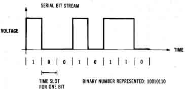
Figure 5-18. Many digital systems transfer data in serial form.
Each bit of the binary number is sent one after another.
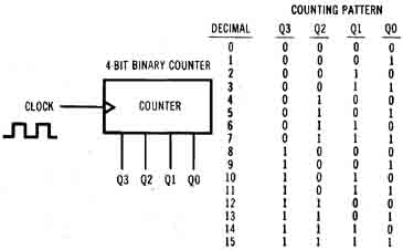
Figure 5-19. A 4-bit binary counter counts the number of rising
edges on the clock input.
Some typical voltage waveforms are shown in Figure 5-21. The key to understanding the circuit operation and the waveforms is to focus in on the rising clock edges. Only at these times can the output change state. On the first rising edge of the clock, Q changes from 0 (its previous state) to 1 (the logic level currently present at the D input). Q stays in this state until the second rising clock edge at which time D is 0, so Q becomes 0. Notice that although the logic level at the D input changes several times, these changes are transferred to the Q output only upon a rising edge of the clock. Also, no action occurs on the falling edge of the clock.
From the preceding examples it's apparent that digital circuit operation can produce some very complex waveforms. Although these wave forms are digital in nature, there still exists a need to examine their voltage and timing characteristics. Clearly, a multiple-channel oscilloscope would be of great value. Adjusting the trigger for a stable display is often a problem, since the waveforms may not be constant. (Try experimenting with the trigger level and slope as well as changing the trigger source.) Single-sweep capability (preferably with storage) is useful for capturing transients.
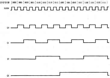
Figure 5-20. The voltage waveforms for a 4-bit digital counter,
assuming the counter is initially in the zero state.
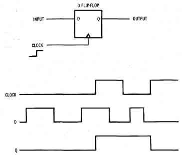
Figure 5-21. The Q output of a D flip-flop changes to the same logic
level as the D input whenever a rising edge of the clock occurs.
Frequency-Response Measurement
Earlier in the section, gain and phase measurements were discussed as applied to a single frequency. A single-frequency sine wave was connected to the input of a circuit and the gain through the circuit, as well as the phase of the output signal (relative to the input), were measured. This describes the behavior of that circuit at that particular frequency, but it's often desirable to characterize the circuit performance over a wide range of frequencies. The gain and , to a lesser extent, phase measured at a range of frequencies is called the frequency response of the circuit.
Frequency Response from Single-Frequency Measurements
The most obvious way to measure the frequency response of a circuit is to perform multiple single-frequency gain (and phase) measurements, and plot them as gain vs. frequency and phase vs. frequency. For example, Figure 5-22 shows a simple RC low-pass filter being driven by a sine wave source. The oscilloscope is connected such that it measures the input voltage and output voltage of the circuit. The resulting voltage measurements at the input and output for a variety of frequencies are tabulated in Table 5-1. Note that if only the gain is required, then other instruments such as a voltmeter could be used to measure Vin and Vout . One might be tempted to assume that Vin will always be constant, but this will not necessarily be true. Vin can change due to source flatness and /or loading effects changing with frequency.
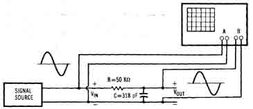
Figure 5-22. An example of a frequency-response measurement.
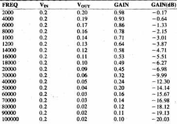
Table 5-1. Measured Values Used to Determine the Frequency Response
of the RC Filter.
The gain for each frequency is calculated by dividing the output 0 by the input voltage at that frequency. The frequency response can then be plotted as shown in Figure 5-23. Alternatively, the frequency response can be plotted in decibels on the vertical axis, and the logarithmic frequency on the horizontal axis. Since the dB scale is inherently logarithm this results in a log vs. log plot. This logarithmic scale has the effect of showing widely varying gain values on a compact plot. Notice that the frequency scale of Figure 5-24 easily accommodates several decades of frequency, while the linear scale used in Figure 5-23 does not.
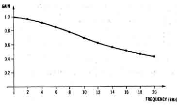
Figure 5-23. The frequency response of the RC filter plotted as linear
gain vs. linear frequency.
Swept Response
Although the previously described point-by-point method is valid and produces accurate results, it's somewhat time consuming. Another method of measuring frequency response involves using a sweep generator to speed up the measurement. The swept sine wave of the sweep generator is connected to the input of the circuit under test (Figure 5-25). The output of the circuit under test is connected to the vertical channel of an oscilloscope operating in the X—Y mode. The sweep voltage of the sweep generator drives the horizontal axis of the scope. As the sweep generator sweeps in frequency, the sweep voltage of the generator ramps up (in proportion to frequency), causing the output of the circuit under test to be plotted across the scope display. In this manner, the entire frequency response of the circuit is quickly displayed on the scope (Figure 5-26).
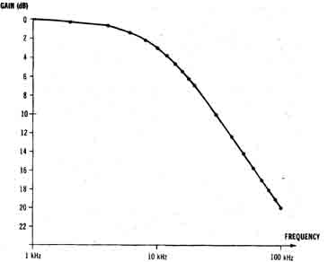
Figure 5-24. The frequency response of the RC filter plotted as
gain in decibels vs log frequency.
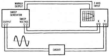
Figure 5-25. A sweep generator and a scope operating in X—Y mode
can be used to automatically plot the frequency response of the circuit.
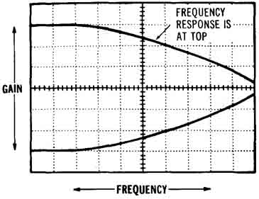
Figure 5-26. The oscilloscope display of the swept- frequency response.
The vertical axis is Vo and the horizontal axis is the frequency range
swept by the generator.
This method relies on the output of the sweep generator being constant with frequency. The flatness of the generator will cause an error in the frequency response. Also the drive capability of the generator is important. The load that the circuit places on the generator will usually vary over frequency. The generator must be relatively insensitive to these load changes or another error will be introduced. For both of these reasons it's a good idea to check (with the scope) to make sure that V is constant as the generator sweeps.
The oscilloscope is displaying Vout and not the gain (Vout / Vin ). If Vin was set up to be a convenient value (such as 1 volt) then the display can be interpreted directly as gain. Otherwise, a small amount of mental arithmetic may be necessary to convert the Vout display to actual gain.
The sweep generator should not be swept too fast, since the circuit under test needs time to respond. This is particularly important in circuits with abrupt changes in gain as the frequency varies. The sweep rate for the generator is usually set experimentally by reducing the sweep rate until the frequency response no longer changes with each change in sweep rate. The sweep generator may be swept in either a linear or logarithmic manner, depending on the desired type of frequency axis. The oscilloscope vertical axis is, of course, always linear.
Sometimes we desire to locate a particular point on the frequency- response curve very precisely with respect to frequency. Thus, many sweep generators supply a marker output signal which pulses when a particular frequency (or frequencies) is present at the generator output. This signal can be connected to the Z axis input of the oscilloscope. The sweep generator will pulse the marker output, causing a change in intensity on the oscilloscope display at precisely the marker frequency. Exactly how the intensity changes (whether it gets brighter or dimmer) will depend on the polarity of the marker signal as well as the polarity of the Z axis input. Another type of marker function is sometimes provided which pulses the output voltage slightly at the marker frequency. This causes a “blip” to appear on the display at the marker frequency. The Z-axis input is not used in this case.
Square Wave Testing
Sine waves are the predominant signal for characterizing the frequency response of analog circuits, but the square wave can also be used. This technique is valid only for devices with flat frequency responses, such as audio amplifiers. (A fairly standard test for audio equipment is a 1 -kHz square wave test.) In addition, the circuit under test must be DC coupled. One special case of square wave testing is the compensation of attenuating probes already discussed in Section 4.
A square wave is applied to the input of the circuit being tested and the output of the circuit is monitored on an oscilloscope (Figure 5-27). The square wave, as discussed in Section 1, is very rich in harmonics extending out to many times its fundamental frequency. The relative amplitude of each of these harmonics must remain unchanged for the output to be a square wave. If the circuit under test is an amplifier, the amplitude of each harmonic will be increased by the amplifier’s gain, but the amplitudes of the harmonics relative to each other should remain the same. In addition, each harmonic has a particular phase relationship with the fundamental frequency that must be maintained. Otherwise, the out put will not be a true square wave. The circuit could even have a perfectly flat amplitude response, but not pass a square wave correctly due to phase distortion. This type of test requires a high quality wave form at the input, otherwise the output square wave will also be de graded. Depending on the output characteristics of the generator, the circuit under test may load the generator enough to cause distortion. It is usually a good idea to monitor the input waveform with the second channel of the oscilloscope.
Although the square wave test does not result in a frequency-response plot, it does test a circuit quickly, with good qualitative results. Some typical output waveforms encountered in square wave testing and their causes are shown in Figure 5-28. Phase shift at low or high frequencies can cause a tilt to one side or the other of the square wave. It is difficult to predict the effects of attenuation at either high or low frequencies as it depends greatly on the exact shape of the frequency response. However, a few typical examples are shown. Some circuits will exhibit a noticeable degradation in the rise time of the output square wave. This is referred to as slew-rate limiting. Due to the nature of the square wave test, it's more effective at determining whether a problem exists than identifying the particular problem.
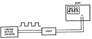
Figure 5-27. The square wave test of a circuit is a good, qualitative
test of a circuit’s frequency response.
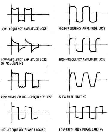
Figure 5-28. Some examples of waveforms resulting from the square
wave test.
Linearity Measurement
It is often desirable to measure the DC output voltage of a circuit com pared to the DC input voltage. This can be done using the X—Y mode of the oscilloscope as shown in Figure 5-29. A slowly varying DC voltage is applied to the input of the circuit as well as to the X axis of the scope. A convenient method of obtaining the varying DC voltage is to use a triangle wave with a very low frequency. The output of the circuit is connected to the Y axis of the scope, resulting in the output voltage being plotted vs the input voltage. The frequency of the generator is chosen high enough so that the display does not flicker too much, but low enough so that the operation of the circuit is not affected. (Remember, a DC voltage is being simulated.)
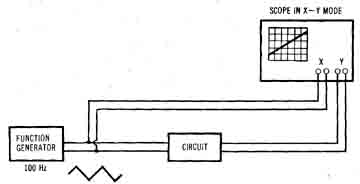
Figure 5-29. The oscilloscope can be used to measure the DC linearity of a circuit.
Consider the clipping circuit shown in Figure 5-30. For a Vin of less than 5 volts and greater than zero volts, the zener diode acts like an open circuit, and Vout , is equal to Vin . When Vin becomes greater than 5 volts (the zener voltage), the diode turns on and Vout , is limited to 5 volts, no matter how large Vin gets. If Vin becomes less than zero, the diode turns on in the other direction and limits Vout to zero volts. (Actually, it would limit the voltage at a slightly negative value, typically -0.6 volt, depending on the diode.) At any rate, the effect of the circuit is to limit the output voltage to between about 0 and 5 volts.
If a DC linearity measurement were made on the circuit using the technique described, the display would appear as shown in Figure 5-31. The sloped portion of the trace corresponds to the region where Vout , equals Vin . The two flat parts of the trace are where Vout , is limited by the clipping action of the circuit.

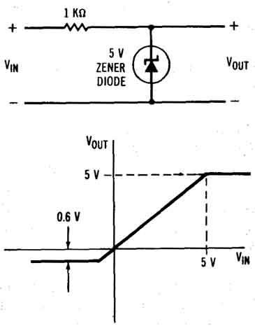
Figure 5-30. This circuit limits the output voltage to be between 0 and 5 volts.
Figure 5-31. The Vout vs Vin linearity display for the clipping circuit.
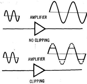
Figure 5-32. Clipping occurs at the output of an amplifier when
the amplifier can't produce the peak voltage of the waveform.
With an amplifier, it's usually desirable to have the output always equal the input, but amplified by some amount. Thus, the output wave form is the same as the input waveform, except with a larger amplitude. For increasingly larger input voltages, the amplifier will at some point stop producing a proportionally larger output voltage. At this point, the output waveform will be clipped (Figure 5-32). The peaks of the wave form are flattened out at this output level.
The Vout vs Vin linearity plot of the amplifier can also be used to measure this phenomenon (Figure 5-33A). The display is a straight line whose slope is the gain of the amplifier. Ideally, the straight line of the display would extend indefinitely. That is, the amplifier would be cap able of amplifying any input voltage, no matter how large. In reality, the amplifier will clip at some point, usually as the peak voltage approaches the amplifier’s power supply voltage, as shown in Figure 5-33B. The straight line is still present, but flattens out at the point of limiting. Typically, the trace does not break sharply, but instead is rounded off.
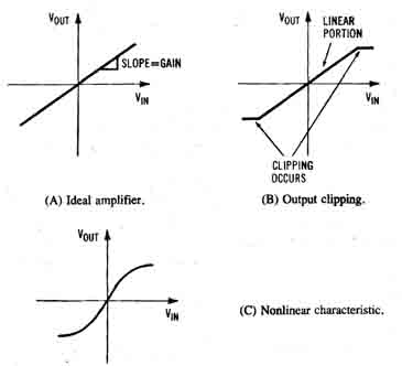
Figure 5-33. The Vout vs V plot for an ideal amplifier is a straight line.
Since the Vout vs Vin characteristic is a straight line, this type of circuit operation is called linear. If the plot is not a straight line then the characteristic is termed nonlinear (Figure 5-33C). Nonlinear amplifier operation causes distortion of the output signal (usually in the form of harmonics).
Curve Tracer Measurement Technique
Another useful oscilloscope measurement technique is the curve tracer circuit. This technique uses the oscilloscope in X—Y mode to display the current through a component (such as a resistor or diode) vs the voltage across the component. This display is referred to as the I-V (current- voltage) characteristic of the component.
There are several ways to make this measurement. Figure 5-34A shows a function generator driving the curve tracer circuit. V is the voltage across the device being measured and V is the voltage across the resistor. By Ohm’s law, V will be proportional to the current through the resistor, which is also the current through the component under test. So if V could be displayed vs V the I-V characteristic of the component would be shown. If the scope has floating inputs, then this can be done with no problem.
Unfortunately, most scopes have grounded inputs which results in the situation shown in Figure 5-34B. Both sides of the component under test are grounded, resulting in a short circuit across it. The situation is com pounded even further if the source has a grounded output. If the source is floating, then the circuit in Figure 5-34C can be used. Note that the circuit ends up being grounded at only one point, which is where both scope input grounds are connected. Something has changed, though. The horizontal axis of the scope will be -V (instead of + V due to the reversal of the horizontal input leads. This can be compensated for if the scope has an “Invert Channel” switch; otherwise, the I-V curve will appear backwards on the display (left half of the display swapped with the right half). This may be acceptable if the user is willing to mentally convert it back.
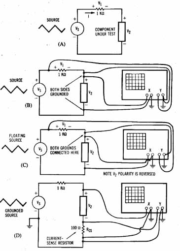
Figure 5-34 Methods for displaying the I-V characteristic of a component.
(A) The approach suitable for use with floating scope inputs. (B) Grounding
problem with typical scope with grounded inputs. (C) An approach for
use with a floating source. (D) Use of a current-sense resistor.
If both the scope and the source are grounded, another technique must be used. A current-sense resistor is placed in series with the component under test. The vertical scope input then uses the voltage across this resistor to measure the current. The voltage across the current-sense resistor will introduce a small error in the measurement of V but as long as the resistor is kept small, the error will be acceptable. The resistor can't be made too small since for a given current being measured, the voltage will decrease with smaller resistance. The sensitivity of the scope will ultimately determine how small the current-sense resistor can be made.
An Example: Diode I-V Characteristic
Figure 5-35 shows an oscilloscope set up to measure the I-V characteristics of a diode, using the current-sense method. The source (usually a function generator) is set to produce a low- frequency triangle wave, although a sine wave will also work. The triangle wave acts as an automatic varying DC voltage, causing the voltage across the diode to also change. At the same time, the voltage across, and the current through, the diode are measured. The amplitude and frequency of the function generator can be set experimentally, but a zero-to-peak voltage of 5 volts and a frequency of 30 Hz is a good starting point.
Figure 5-35. The I-V characteristic of a diode can be measured using the curve tracer circuit with current-sensing resistor.
The resulting I-V characteristic for a diode is shown in Figure 5-36. The horizontal scale can be determined directly from the volts/div set ting. The vertical scale must take into account the value of the current-senses resistor.
amps per div = (volts per div)/Rcs
where
Rcs is the value of the current-sense resistor.
The resulting curve is the classical behavior of the solid-state diode. For voltages greater than zero (right half of the display), the current quickly increases. For voltages less than zero (left half of the display), the current is essentially zero. So the diode conducts in the forward direction, but acts like an open circuit in the reverse direction.
The scope display may actually show two separate traces instead of the single curve. One trace is drawn as the voltage increases, and the other is drawn on the decreasing portion of the triangle wave. They may be slightly different due to either capacitive effects or heating of the component being tested. Reducing either the frequency or the amplitude of the triangle wave will cause the two traces to converge into one single trace.
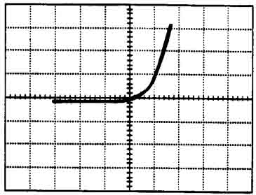
Figure 5-36. The I-V curve of a solid-state diode.
Resistor I-V Characteristic
Worth noting at this point is that the curve tracer circuit can be used to measure unknown resistors. The resulting I-V curve is shown in Figure 5-37. The current-sense resistor, Rcs should be chosen to be at least a factor of ten smaller than the unknown resistance. The voltages shown in Figure 5-37 (Δ X and Δ Y) should be determined, taking into account the volts/div settings. The resistance value is determined by calculating 1/ slope of the line, using the equation shown below.
R = 1/slope
R = Rcs / Δ X / Δ Y
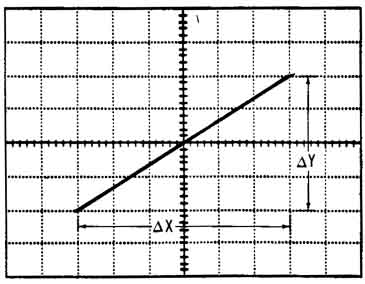
Figure 5-37. The I-V curve of a resistor is a straight line with R = 1/slope.
PREV: Oscilloscopes
NEXT: Miscellaneous Electronic Instruments