AMAZON multi-meters discounts AMAZON oscilloscope discounts
Frequency Counters
As covered in Section 1, the frequency of a periodic waveform is de fined as the number of cycles that occur per second. A convenient and accurate way of measuring frequency is using a frequency counter. A frequency counter uses a precise internal time base and digital counters to produce a digital frequency readout. The measurement is usually as simple as connecting the frequency counter to the signal being measured and reading the digital display.
Figure 6-1 shows a simplified block diagram of a frequency counter. The signal being measured is amplified and changed into a digital pulse train. This pulse train passes through an electronic switch and drives a series of decimal counters. If the switch is closed, the value of the decimal counters will increase by one for each new cycle of the signal being measured. If the switch were to remain closed, the digital counter would keep counting up indefinitely (or at least until it ran out of digits). Instead, the switch is closed for a known length of time and the resulting number of cycles of the waveform is measured. This number represents the frequency of the waveform. For example, suppose that the length of time that the switch is open is 1 second. Then the number of cycles per second (or frequency in hertz) would be displayed on the decimal counter. To perform another measurement, the digital counter is reset and the electronic switch is once again opened. The measurement time of one second was chosen for simplicity. Other measurement times will be used to increase the measurement range of the frequency counter. A typical frequency counter is shown in Figure 6-2.
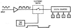
Figure 6-1. A simplified block diagram of a frequency counter.
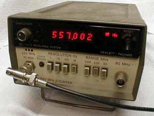
Figure 6-2. A typical 80-MHz frequency counter with both frequency and period measurement functions.
Frequency Dividers
A frequency divider is used to reduce the frequency of a digital signal. Figure 6-3A shows a frequency divider which divides the input frequency by 2 to produce an output frequency at half the input frequency. Similarly, Figure 6-3B shows a divide-by-b circuit which reduces its input frequency by a factor of ten. Notice that both the input and output of the divider is a pulse train. This type of circuit can be used to increase the range of a frequency counter in two ways.
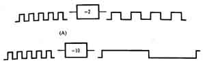
Figure 6-3. A frequency divider produces an output frequency which
is equal to the input frequency divided by an integer number.
(A) A divide-by-2 frequency divider. (B) A divide-by-10 frequency divider.
Figure 6-4 shows a divide-by-10 circuit added to the frequency counter in two different places. At the input, the frequency divider has the effect of increasing the maximum measurable frequency by reducing incoming signals to a range that's usable by the basic frequency counter. In this mode, frequency dividers are often referred to as pre-scalers. For instance, the basic frequency counter may have a maximum frequency limitation of 10 MHz. Adding a divide-by-10 circuit in front of the basic counter extends the range by a factor of 10, to 100 MHz.
The other frequency divider was added to the time-base circuit. This has the effect of increasing the length of time that the electronic switch is on, which means that lower frequencies can be measured than with the original frequency counter.
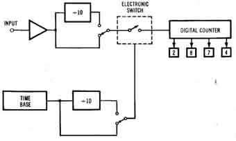
Figure 6-4. A block diagram of a frequency counter showing the use
of frequency dividers to increase the frequency range of the basic
counter.
In both cases, the frequency divider is shown as being able to be switched in and out of the circuit. Typically, several divider circuits are supplied so that the user can conveniently select a measurement range on the instrument. Sometimes a special high-frequency pre-scaler is offered as an external option that increases the high-frequency range of a counter.
Period Measurement
The period of a waveform can be determined mathematically from its frequency (f = 1/T), but the function is often built into a frequency counter. Figure 6-5 shows a small, but important change in the basic frequency counter block diagram—the input and time-base connections are interchanged. In this mode, the input closes the electronic switch for one of its cycles. During this cycle (which is the period of the input), the number of time-base clocks are counted. Suppose the time-base period was 1 msec, then the resulting display would be the number of 1 msec cycles that occurred during one cycle of the input waveform. Put simply, this is the period of the input waveform in msec. By using selectable frequency dividers, other time-base frequencies are easily generated, resulting in other ranges of period measurement.
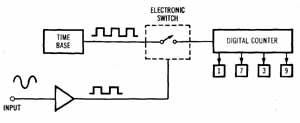
Figure 6-5. The simplified block diagram of a frequency counter
while measuring the period of the input waveform.
Time-Base Accuracy
The time base of a frequency counter is usually a precisely controlled crystal oscillator, which is divided down to produce the needed frequency. This results in a measurement accuracy that's limited only by the stability and accuracy of the crystal oscillator. Since this oscillator must operate at only one frequency, it can be designed to be extremely stable.
Input Impedance
Frequency counters generally have either a 50-ohm or a 1-megohm input impedance. Like several of the instruments already discussed, the 1-megohm input is convenient for general purpose low-frequency measurements. The 50 ohms becomes necessary as higher frequency measurements are made (typically greater than 50 MHz). Since a frequency counter is interested only in frequency (and not amplitude or voltage), a decreased signal level does not immediately reduce measurement accuracy. Thus, capacitive loading due to the 1-megohm input may reduce the signal level into the frequency counter somewhat without introducing error into the measurement. At some point, however, the signal will be attenuated so much that the counter can no longer detect its frequency accurately. Various combinations of 50-ohm and 1-megohm inputs exist. Some counters include both, with the 1-megohm input intended for low-frequency operation, and the 50-ohm input used for high-frequency operation. Other counters have one input that's switchable between 1 megohms and 50 ohms.
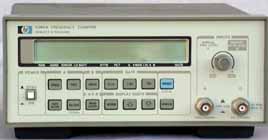
Figure 6-6. A typical 225-MHz frequency counter having both 50-ohm and 1-megohm inputs.
Frequency Counter Specifications
The specifications for a typical frequency counter are given in Chart 6-1. The frequency range is shown as dependent on which input impedance is being used. The sensitivity specifications defines how small of a signal can be measured. Frequency resolution determines how well small of changes in value can be detected.
Chart 6-1. Typical Frequency Counter Specifications
Frequency Range: 10 Hz to 100 MHz (1-Megohm input) 50 MHz to 225 MHz (50-ohm input)
Input impedance: 1 Megohms with 25-pF capacitance in parallel 50 ohm
Sensitivity: 20 mV RMS
Frequency Resolution: 8 digits
Temperature Stability: < 2 ppm, 0 to 40 deg C
Aging Rate: < 0.1 ppm/month
The most desirable specification is conspicuous by its absence. There is no frequency accuracy spec. This seems a bit strange at first, until one understands what limits the performance of the instrument. If the time- base of a frequency counter is adjusted to be exactly on frequency, presumably by comparing it to some perfect frequency standard, then there is essentially no frequency error at that instant in time. However, over any time interval the time base will tend to drift in frequency, primarily due to aging effects in the crystal oscillator and changing performance with temperature. Fortunately, the aging and temperature stability are usually specified by the manufacturer.
Consider the typical specifications given in Chart 6-1. Ignoring temperature changes for the moment, the long term frequency stability will be determined by the aging rate (0.1 ppm/month). Assuming the frequency counter was adjusted to be exactly on frequency (to within the resolution of the counter) at some point in time, then one month later it may be off by as much as 0.1 part per million. For a frequency of 100 MHz, the maximum error would be 10 Hz. One year later, the frequency could be off as much as 12 X 0.1 ppm = 1.2 ppm. This results in an error of 120 Hz on a 100 MHz signal. Similar calculations can be made for the effect of temperature stability.
Receiver Comparison Method
A heterodyne receiver with a product detector may be used to measure the frequency of a signal. Communications receivers that are capable of receiving CW (continuous wave) or SSB (single sideband) signals fall into this category. The receiver is tuned to the approximate frequency of the signal which should result in a steady audio tone out of the receiver.
The frequency of the audio tone is the difference between the receiver’s frequency and the signal frequency. As the receiver is tuned closer and closer to the frequency of the signal, the audio tone will decrease in frequency (become a lower tone). At some point around 20 to 40 Hz, the audio tone will disappear as it falls below the normal human hearing range. This process of tuning the receiver for zero frequency difference is known as zero beating.
If the frequency dial or readout of the receiver is accurate enough, then the process of zero beating the signal may be a suitable means of measuring the frequency of the signal. As modem receiver design has improved, very stable receivers with precise digital frequency readout are available. Periodically, the receiver must be calibrated using an external frequency reference to correct any long term drift (Figure 6-7). If the receiver’s stability is excellent then this may be required only rarely. However, if the receiver can't maintain a constant frequency then calibration will be required before every frequency measurement.
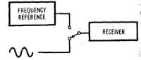
Figure 6-7. An accurate frequency measurement can be made using
a stable communications receiver and an accurate frequency reference.
Frequency References
The most obvious frequency reference is a very accurate sine wave source. A sine wave with known frequency can be connected to the input of the receiver and the frequency calibration adjustment can be tweaked to put the receiver on frequency (using the zero beat technique).
Another type of frequency reference is the crystal calibrator. The calibrator uses a crystal oscillator to produce signals at precise frequencies spaced at some frequency interval (typically 50 or 100 kHz). This is easily done by creating a periodic signal at 100 kHz which has harmonics extending out to the highest frequency of interest. This produces a lot of signals for the receiver to choose from, but the receiver is presumably accurate enough to know which multiple of the calibrator frequency it's tuned to. Crystal calibrators are becoming less common on communications receivers as frequency synthesis techniques allow the receiver to derive its frequency directly from a crystal-controlled oscillator.
An even better and usually convenient frequency reference is pro vided by the National Bureau of Standards (NBS) or similar governmental agency. The NBS operates two radio stations, WWV located in Ft. Collins, Colorado and WWVH located in Hawaii. In addition to transmit ting precise time information, the frequency of the radio transmitters are accurate to one part in 1011. These stations transmit on standard frequencies in the high-frequency band at 2.5 MHz, 5.0 MHz, 10 MHz, 15 MHz and 20 MHz (WWV only). Depending on propagation conditions and the receiver’s geographical location, at least one of these signals will usually be available at any time. The receiver can be tuned to the nominal transmitter frequency and then the frequency calibration adjustment can be used to zero beat the receiver.
Logic Probes
A logic probe is a small instrument built into a probe-sized case for checking out digital circuits. Generally, a logic probe indicates whether the voltage present corresponds to a logic high or a logic low. The actual voltage of the signal is not displayed, since it's not significant except whether it’s above or below the logic thresholds. Better probes also provide a pulse indicator, which flashes if valid logic pulses are present. Detailed information such as duty cycle or period can't be accurately determined with a logic probe, but the presence or absence of a stream of bits can easily be found. The specifications of a typical logic probe are shown in Chart 6-2.
Chart 6-2. Specifications for a Typical Logic Probe
Frequency range: 0 to 50 MHz
Minimum Detectable Pulse Width: 10 ns
Input Impedance: 2 megohms
Logic Thresholds:
TFL: High=2.4 V, Low=0.8 V
CMOS: High = 70% of supply voltage Low = 30% of supply voltage
Logic Thresholds
The logic probe must be set up to detect the logic levels using the appropriate logic thresholds for the logic circuits being measured. These levels were defined in Section 1. Generally, the most common digital technology is TTL (Transistor-Transistor-Logic), followed by CMOS (Complementary metal Oxide Silicon ). Sometimes these two are lumped together in the same category called 5 volt” logic. This is misleading since although both TTL and CMOS can operate using 5-volt supplies, the logic thresholds are wt the same. In order to accommodate both technologies, many logic probes are switchable between TTL and CMOS. Regardless of the type of probe, it's important that the probe’s logic thresholds match the logic family being tested.
Logic probe Indicators
Different logic probes provide different types of logic state indication. The following list is roughly in order of most common to least common.
Logic High—Indicates that the voltage is greater than high-logic threshold, therefore it's a valid high logic signal.
Logic Low -- Indicates that the voltage is less than the low-logic threshold, therefore it's a valid low logic signal.
HighState -- Indicates that the voltage is neither a logic low nor a logic high. Normally, this means that the digital gate is in the high-impedance state (tri-state) or that the logic probe is not connected to the output of the gate (open circuit). The high-impedance state may be indicated by the absence of both the logic high and the logic low indicators.
Pulse -- Indicates that the voltage is changing from a valid low logic level to a valid high logic level (or vice versa). Often the regular logic low and logic high indicators are flashed on and off when a pulse occurs. The better logic probes provide pu1se circuitry which catches very short pulses and lights the indicator long enough for the human eye to detect it. Without this special circuitry, short pulses might go undetected by the user, even though the logic level indicator was on for a brief time.
Pulse Memory -- Indicates that a pulse has occurred since the last time the memory was cleared. This is very useful for cases where a digital pulse comes along infrequently but must still be detected. The probe is connected to the circuit and the clear button is pressed, clearing the pulse memory. The indicator stays off until a pulse comes along, then the indicator comes on and stays on until cleared again.
Oscilloscope vs Logic Probe
At first glance, it looks like a logic probe would not be needed if an oscilloscope is available. This is somewhat true, but the logic probe does have some advantages over the oscilloscope. The oscilloscope gives more information than is required for troubleshooting a digital circuit. Having the voltage waveform displayed, including all if its imperfections, may make it more difficult to troubleshoot a logic circuit. With a logic probe, the user is sheltered from all of the analog information but is given the digital information. The user does not have to memorize the logic thresholds of the particular technology being used, but instead just looks at the indicator on the probe to determine the logic state. Of course, if the analog behavior of the circuit is in question (such as too much overshoot or glitching), then an oscilloscope is quite useful.
The other advantage that the logic probe has over the oscilloscope is when very short pulses need to be detected. If a scope is used, the triggering and sweep controls must be adjusted to display the pulse properly. This may be tricky, particularly if the pulse occurs infrequently. If the scope does not have display storage capability, when the pulse does finally occur it will be a brief flash across the screen (usually at just the time that the user blinks). With a logic probe, the logic levels are already set up so there is no triggering problem. The pulse indicator will detect pulses that are extremely short and display them long enough for a human to see the indicator. If that's not sufficient, then a probe with pulse memory capability can be used to catch the pulse.
Power Supplies
Power supplies don't measure circuit parameters such as voltage and current, but instead supply circuits with DC voltage and current. Most electronic circuits require a DC voltage to operate. This can be supplied using a battery, a built-in power supply that changes AC voltage to DC voltage, or a bench DC supply. For portable applications, the battery is a good solution. For circuits that are used where AC power is available, having a built-in power supply makes sense. But when designing or testing a circuit, a bench DC supply will usually be the most convenient.
Power supplies may either be fixed or variable. As the name implies, a fixed power supply has a constant output voltage. An adjustment may be supplied on a fixed power supply to precisely set the output voltage. Since the adjustment range is only 5 or 10 percent around the nominal value, the supply is still considered to have a fixed voltage.
Variable supplies can be adjusted from the front panel to produce a wider range of voltages, typically 0 to 20 volts or more. This type of supply is more versatile since the voltage can be set to match the particular circuit requirement. In addition, the voltage can be varied around the nominal value during design or testing.
The circuit diagram for a simple power supply is shown in Figure 6-8. The AC line voltage (typically 115 volts RMS) is connected to the transformer which steps down the voltage to something closer to the final DC value. The diode (or rectifier) changes the AC sine wave voltage into a half sine wave. The filter capacitor smooths out the half sine to approximate a DC voltage. This DC voltage is not well controlled so it's passed through a circuit called a voltage regulator which precisely controls the output voltage. This is one of the simplest types of power supplies, shown here to briefly introduce the steps necessary to change AC into DC.
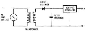
Figure 6-8. Schematic diagram of a simple power supply.
Power Supply Specifications
There will be imperfections in the DC voltage. There will be a small amount of AC ripple remaining riding on top of the DC (Figure 6-9). The AC ripple is a remnant of the AC line voltage which is not removed by the filter capacitor and voltage regulator. The ripple will be at the line frequency (usually 60 Hz in the U.S.) plus the harmonics of the line frequency (120 Hz, 180 Hz, etc.). Some power supplies use regulation techniques that will cause other frequencies to be present. In a quality power supply, all of these ripple components will be low enough that they can usually be neglected (less than a few millivolts).
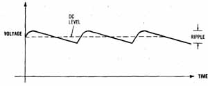
Figure 6-9. The DC output voltage of a power supply will have some
small amount of AC ripple present.
The DC voltage may vary as the amount of current drawn from it changes. The regulation specifications of the power supply describes how much the output voltage may vary under operating conditions. Load regulation (also called load effect) is how much the supply voltage varies with change in power supply load.
LOAD REG = VNO LOAD — VFULL LOAD
VNO LOAD is the output voltage without a load connected, while VFULL LOAD is the output voltage at the maximum load current (full load). Line regulation (also called source effect) is the amount that the output voltage varies due to changes in the power line voltage (over a specified range). Both types of regulation may be expressed as a voltage or as a percent of the output voltage.
A good power supply provides built-in current limiting and short-circuit protection. This means that if the output of the supply is accidentally shorted out (and it will be), the supply reduces its voltage to prevent excessive amounts of current from being drawn. This protects the supply itself and , to a lesser extent, the circuit under test. The current limit may be adjustable so the trip point can be customized to the circuit at hand. The current limit should usually be set just high enough to allow proper circuit operation (with some margin). That way, normal circuit operation is allowed but short circuits will not draw any more current than necessary. This is most important when using supplies capable of supplying high current.
Circuit Model
The simplest circuit model for the DC power supply is just a DC voltage source (Figure 6-10A). With this model, no matter what else happens, the voltage across the two terminals is always the DC value of the voltage source. This is precisely what is desired in a voltage source—a constant DC voltage—and this circuit model is valid for many applications.
A more realistic circuit model, including the internal resistance of the power supply, is shown in Figure 6-10B. This resistance corresponds to the phenomenon that as current is drawn from the power supply, the output voltage decreases. For a good power supply, this resistance value is very small (typically less than an ohm). As a side note, this circuit model is also applicable to batteries.
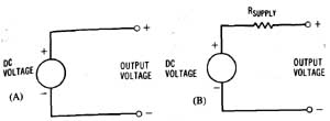
Figure 6-10. Circuit models for a DC power supply.(A) The
simplest model. (B) A model including the internal resistance of the
power supply.
Just as with signal sources and oscilloscopes, the grounding of a power supply output must be understood. Figure 6-11 shows the output connectors of a typical power supply. Three terminals are provided: the + and - terminals are the two connections for the output voltage, and the third terminal is the ground connection. If the ground connection is left disconnected, the power supply’s output is floating. That is, both the + and the - terminals can be connected anywhere in the circuit without regard to grounding. If the ground terminal is connected to the - terminal, then the power supply is grounded. A grounding strap that connects the two terminals is sometimes supplied for this reason. Some supplies are inherently grounded and will not allow the negative terminal to be at any electrical potential other than ground.
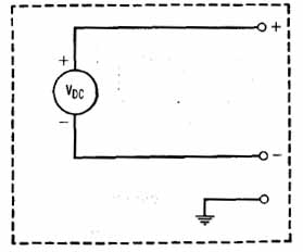
Figure 6-11. Circuit model for a floating power supply with optional
ground connection.
Some electronic circuits (operational amplifiers, for instance) require both positive and negative power supply voltages. These two supplies are often built into one bipolar supply. The circuit in Figure 6-12 shows how the two supplies are connected internally. The supplies shown are floating but can be grounded as needed by connecting the common terminal to the ground terminal. Figure 6-13 shows how two single power sup plies can be connected to produce a bipolar power supply. At least one of the power supplies must be floating to avoid any conflicts in grounding.
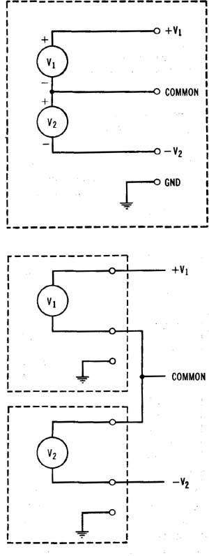
Figure 6-13. Two single power supplies can be connected to create
a bipolar supply.
Figure 6-12. Circuit model for a bipolar floating power supply.
PREV: Oscilloscope
Measurements
NEXT: Circuits for Electronic
Measurements