AMAZON multi-meters discounts AMAZON oscilloscope discounts
Introduction:
Most of the applications of linear electronic circuits are in the amplification of alternating electrical signals, of sinusoidal, or similar repetitive form, and it will usually have been necessary, at some earlier point in the system, to generate this signal, either as the output of some electro-mechanical transducer, or from some other electronic circuit arrangement.
Repetitive signals, of sinusoidal or other forms, may also be used as a means of testing equipment which is intended for use in other applications. In this case, the kind of signal which is used will depend on the type of test which is to be made. Nearly all of the oscillators and signal generators used in electronic circuitry are based on the use of positive feedback -- see Section 7 -- from the output of an amplifying or impedance converting stage back to its input, though there are a few exceptions to this, as in negative impedance oscillators and 'noise' sources, which will be considered later.
Sinewave oscillators:
A number of techniques have been evolved for generating pure (i.e. noise, hum, and harmonic free) sinewave signals, of which the most common is to pass the feedback signal from a low distortion amplifier through a phase-shifting network chosen so that the required 360° loop phase shift is provided. These are generally classed as 'phase shift oscillators', even though, for example, in the case of the Wien Bridge and similar systems, the condition required of the RC network is that it should provide zero phase shift at the required operating frequency.
For a pure sinewave output, assuming a distortion free amplifier block, the gain of the system must be adjusted so that the overall feedback loop has unity gain, or either the system won’t oscillate at all, or the amplifier will be driven into overload, which will cause the peaks of the output waveform to be clipped.
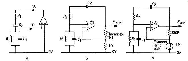
FIG1 Wien bridge oscillator layouts
Phase-shift oscillators
Wien bridge systems:
The simplest style of Wien Bridge oscillator is shown in FIG1a. This design takes advantage of the fact that the Wien network, R1R2C1C2, shown in the practical design given in FIG1b, has zero phase shift, from point ?' to point ?' , at a frequency given by the equation
f0=1/(2 pi CR)
in the case where C1 = C2, and R1 = R2. At this frequency the upper limb, C2R2, has twice the impedance of the lower, C1R1 , so the transmission of the network is 1/3.
If some means is used to adjust the system gain to 3, the circuit will oscillate, and, provided that the amplifier itself is linear, and the output voltage swing is not too large, a low distortion sinusoidal output signal can be obtained.
Clearly, some means for automatically adjusting the loop gain of the amplifier is desirable, and this is commonly done by the use of either a thermistor (TH1), whose resistance will decrease, increasing the amount of NFB and reducing the loop gain, as the output AC signal increases, or a low power filament bulb (LP1, as shown in the design given in FIG1c, whose resistance will increase as the applied AC voltage is increased; which gives the same result.
This type of circuit can be improved by separating out the two portions of the Wien network, as shown in FIG2. In this arrangement, A1 is used as a summing amplifier, combining the negative feedback path through R1C1 with the positive feedback signal through R2C2. The overall loop gain is stabilized, in this case, by connecting a thermistor, TH1 as a negative feedback element across A2.
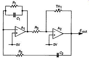
FIG2 improved Wien bridge oscillator
Because both of the amplifiers are operated in the phase inverting mode, so that the 'common mode input' (the signal appearing simultaneously on both the inverting and non-inverting inputs of the amplifier block) is zero, very low orders of harmonic distortion can be obtained from this layout. A typical total harmonic distortion figure for the circuit shown in FIG2 is <0.002% @ 1kHz and IV RMS output.
Lag/lead and lead/lag oscillators:
There are two other layouts, shown in FIGs 3a and 3b, which, for the same R and C values, have identical phase and transmission characteristics to the Wien network, and which can be employed in oscillator systems, as shown in the designs given in FIGs 4a and 4b. Once again, these can be recast in circuit layouts free from common mode distortion effects, as shown in the circuit arrangements, due to the author, of FIGs 5a and 5b. As in the case of the circuit of FIG 2, these designs are characterized by the very low distortion of the output signal, which will consist of third harmonic residues, and be almost entirely due to the amplitude modulation effect, within the waveform, of the amplitude stabilization component.
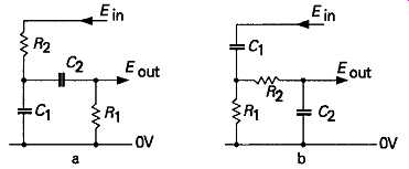
FIG 3 Phase shift networks having an equivalent performance to the Wien
bridge
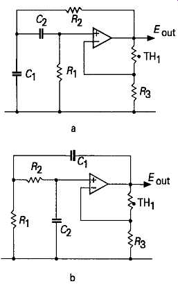
FIG4 Practical oscillator designs based on lag-lead and lead-lag networks
The phase-shift or Dippy oscillator:
This type of design, analyzed fully by Gamertsfelder and Holdam Waveforms, Section 4, MIT/McGraw Hill, 1949), enjoyed considerable popularity some 40-50 years ago, but has now largely been forgotten, though it’s capable of excellent results.
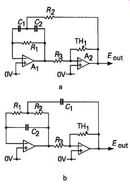
FIG. 5 Rearrangements of lag-lead and lead lag oscillators to avoid common-mode
type distortions
Its method of operation is based on the fact that any simple RC network will give a phase shift of 60° at some input frequency, and that a group of these net works -- at least three are needed -- can therefore be made to give a total phase shift of 180°, to provide the necessary 360° loop phase shift, when connected be tween the output of an amplifying block and an inverting input. There are two ways of doing this, shown in FIGs 6a and 10.6b. If all the values of R and of C are identical, these circuits will oscillate at frequencies given by the equations …

...respectively, and a loop gain of 29.25dB (29) is required.
In any practical design in which the purity of the output waveform is important, the circuit layout of FIG6a is preferable -- in spite of the fact that, for the same operating frequency, it will require the values of the capacitors in the phase shifting chain to be six times greater than that of the layout of FIG6b -
because it has a somewhat lower harmonic distortion, due to greater attenuation of high frequency harmonic components in the RC chain. Also, unless a bridging resistor, Rx, is included in parallel with the CR chain, which somewhat alters the loop gain and the operating frequency, the layout of FIG6b does not provide the DC negative feedback path required to give stability of the amplifier DC level. Automatic control of the system loop gain to sustain oscillation at a suitable level, below the point of overload, can be provided by including a second amplifier, with a thermistor in its feedback path, as shown in FIG6c.
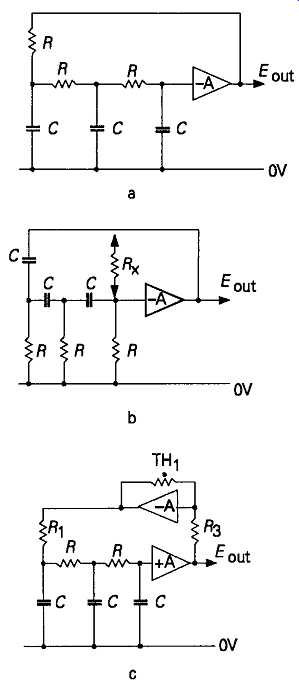
FIG. 6 Phase-shift or Dippy oscillator layout.
A modern version of the phase-shift oscillator is made from a cascaded series of opamps, or digital buffer amplifier ICs, each of which has a capacitor between its output and inverting input, as shown in FIG. 7a. If a CMOS inverter gate is used, the time lags in each of these, due to propagation delays, will allow a phase-shift oscillator without any further components, as shown in FIG. 7b. The operating frequency of such an oscillator is dependent on the supply voltage, allowing its use as a simple voltage controlled oscillator (VCO), but such an oscillator is very temperature dependent, and its long-term frequency stability is poor.
The parallel-T oscillator:
This is a very important type of oscillator, and has the general layout shown in FIG8a. Its method of operation is simply that, since the parallel-T net work will have zero transmission at some specific frequency, depending on the component values, so the amplifier will be free to amplify all those components of circuit noise, which occur at that frequency, with its full open-loop gain. Since all other frequencies will be subject to a large amount of negative feedback, the magnitude of these distortion components will be low.
In reality, though, the method of operation is rather more subtle. Most practical amplifier blocks will have an internal open-loop phase shift of at least -90° over a fairly wide part of their working frequency range, so since the transmission characteristics if the parallel-T shift abruptly from a phase lag of -90° to a phase lead of +90° on transition through the null transmission frequency, as shown in FIG. 9, there will be a frequency, just below the null point, at which the overall phase shift in the feedback loop will be -180°, and the circuit will oscillate.
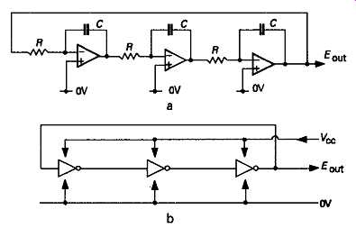
FIG7 Modern versions of phase-shift oscillator circuits.
The circuit can be elaborated slightly, as shown in FIG. 8b, to allow automatic stabilization of the circuit gain. Circuits of this kind can offer very low levels of harmonic distortion, and have formed the basis of commercial ultra-low distortion test oscillator designs.
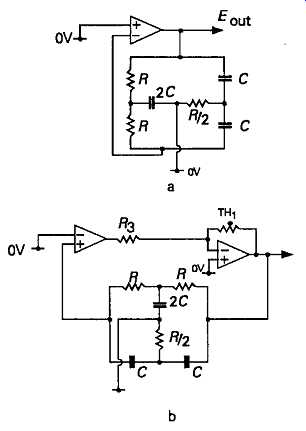
FIG8 Parallel-T oscillator layouts
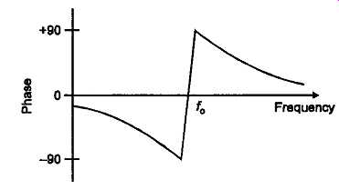
FIG9 Phase shift of parallel-T network on passing through f0
The Fraser oscillator:
This circuit (Fraser, W., Electronic Eng., May 1956), was originally offered as a thermionic valve design, but shown here with opamp gain blocks for simplicity, is based on the use of a pair of all-pass filter networks -- see Section 8 -- each of which will give a phase shift of 90°, interposed between amplifier blocks, as shown in FIG. 10. A third gain control block, A3, can be used, as shown, to stabilize the overall loop gain.
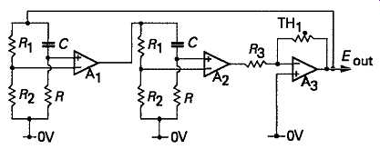
FIG10 The Fraser oscillator
Beat-frequency oscillators (BFOs):
This type of oscillator, which is the pre-eminent choice where a wide output frequency range is to be provided from a single knob frequency control, employs the type of design, shown in schematic form in FIG. 11, in which the outputs from a pair of HF oscillators, OSC1 and OSC2, are combined in a 'sum and difference' frequency generator, PD x, and the resultant output is filtered to remove the 'sum' frequency components. The output 'difference' frequency can then be made to sweep a range from zero up to as high a frequency as is required, depending on the range of the variable frequency oscillator.
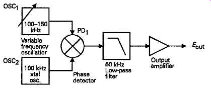
FIG. 11 Layout of beat frequency oscillator
At least one of the input HF oscillators should have a low distortion output if the output signal is to be of high purity, since the difference frequency between any harmonic components present in both oscillators will generate a harmonic component in the output. If one oscillator is harmonic free, the spurious HF signals generated by harmonic components in the other can be removed by subsequent low-pass filtering. To ensure good frequency stability in the final output signal, very high stability is required from the two input oscillators. However, the fixed frequency oscillator can be crystal controlled, which will also assist in achieving a low harmonic content in the output signal.
The function of a sum and difference generator in a BFO can be performed by combining the signals at the input to almost any nonlinear circuit element, but the highest purity in the output difference waveform is best achieved by the use of a 'double balanced modulator' system, such as the Motorola MC 1496 integrated circuit.
Amplitude control and amplitude bounce:
All of the oscillators described above will only give a true, low-distortion, sinewave output if the amplitude of the output waveform is kept within the linear range of the amplifying devices. This requirement generally demands some method of automatic output voltage control, and I have sketched, in several of the circuits shown above, methods, using either negative temperature coefficient thermistors or positive temperature coefficient heated wire systems, by which this can be done. Unfortunately, all high purity sinewave generator circuits simulate, in their characteristics, a high Q tuned circuit (see Section 11), of which one of the most notable characteristics is that its bandwidth, in relation to its operating frequency, is narrow; and the higher the Q of the circuit, the narrower the bandwidth will be. This means that the system will only respond slowly to a change in the magnitude of any input sinusoidal signal applied to it. In this it resembles the operation of an RC integrating network, in which the time constant of integration is related to the Q of the circuit, and to the purity of the output waveform.
It’s also necessary, in any amplitude control system, that there should be a long time constant, typically several seconds, in its response to a change in the signal amplitude, in order to limit the extent to which the wave shape of low frequency signals is distorted by the system gain being modulated by the instantaneous value of the waveform, in terms of its displacement from its mid-point potential. So the control network, itself, is required to simulate an RC integrating network. This leads to the amplitude control system having the general form shown in FIG12, where C1 and R1 represent the effect of the narrow frequency response of the system (related to the sine wave output purity), and C2 and R2 represent the time constant of the thermistor or filament bulb element.
Typically, if a step-function voltage input, shown as line (a) in FIG. 13, is applied to such a feedback system, it will lead to an output response, as shown by the line (b), and this is typical of the behavior of high purity sinewave oscillators following initial switch-on or any subsequent disturbance -- in which the output signal amplitude will exhibit a bounce as a function of time, exactly as shown in FIG. 13b.
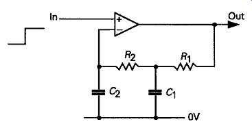
FIG12 Equivalent circuit of low distortion gain stabilized amplifier
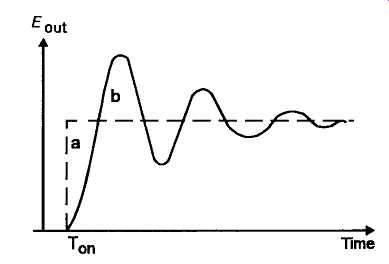
FIG. 13 Output amplitude bounce effect
For any given amplitude control method, the duration of the bounce period, before the oscillator settles down, will lengthen as the purity of the waveform is improved, and as the operating frequency is lowered.
Indeed, the duration of the bounce, in any simple amplitude control system, for any given operating frequency, can be taken as an indication of output waveform purity. This output signal amplitude instability can be a nuisance in practice, especially as an adjustment to the operating frequency in a variable frequency oscillator, is likely to trigger a sequence of amplitude bounces in the output signal.
Various methods have been proposed to avoid this snag, such as the use of two control systems, one to control the amplitude in the normal manner, and the second to 'clip' the output voltage swing at, say, 10% above its normal level: a system which will limit the duration of the amplitude instability.
However, the only really effective system is to use an input waveform which is already amplitude limited, such as an amplitude clipped triangular wave, and then to filter this waveform to remove unwanted harmonics, and to improve its purity.
Relaxation, or capacitor charge/discharge oscillators
This type of oscillator design, in its various versions, can generate a very wide range of output waveforms, almost all of which will be non-sinusoidal. These may be triangular, or 'sawtooth' (a triangular waveform in which the slopes of the 'rise' and 'fall' transitions are not identical), or rectangular, or square-wave (a rectangular waveform in which the ‘on' duration is identical to the 'off' duration -- a condition described as having an equal 'mark-to-space' ratio), or 'stair case, or any combination of these. Most of these circuits were developed for use with thermionic valve gain blocks, though for practical convenience I have shown these, modified as necessary, in their contemporary bipolar transistor, field effect device, or opamp forms. (A useful general survey of the more commonly found types, arranged for use with bipolar junction transistors, is given in the Ferranti 'E-line' transistor application report, 9th Edition, 1980.) It’s perhaps appropriate to note at this point that, in logic circuit nomenclature, free-running waveform generator systems are referred to by the general term 'astable'. Most of these astable designs can be con figured, with some modification in circuit layout, so that they will become 'one shot' oscillators, and be cause of the demands of digital circuit technology there is now a wide range of such triggerable logic function ICs.
However, in order to keep the scope of this guide within reasonable limits, I propose to confine this description to continuous waveform generators, and to omit analysis of those multivibrator or similar systems which are 'mono-stable' -- a term which is used to describe circuit arrangements which will always revert, following a cycle of operation, to some specific 'rest' condition, -- or 'bi-stable' -- a classification which denotes systems which can reside in either of two possible rest states.
The multivibrator
This is one of the longest established of all the rectangular waveform generating circuits, and is represented best, in modern circuit practice, by the junction FET layout shown in FIG. 14. Its method of operation is that, on switch-on, the current flow through one or other of the FETs, Q1 or Q2, will be slightly greater than that of the other, and that, when the voltage drop which this causes, through either R2 or R3, is coupled to the gate electrode of the device passing the lower initial current, by way of C1 or C2, it will cause the current through that device to be reduced still more.
This causes a further reduction in its drain current, and a consequent increase in the forward gate bias of the conducting FET, with the result that the cumulative effects of these changes causes the drain current of one FET to become completely cut off, while the other is passing a value of current which is characteristic of its zero gate bias state.
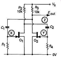
FIG14 Simple FET multivibrator
However, the negative gate bias voltage developed across C1 or C2, in the circuit of FIG14, will decay away with time through R1 or R4, with a time constant dependent on the values of R1/C1 or R4/C2, giving a gate voltage waveform of the type shown in FIGs 15a or 15b. When the voltage has decayed to the extent that the device which is cut off begins to conduct once again, the fall in its drain voltage is coupled to the gate of the conducting FET, causing its drain current to become less, and causing a positive voltage to be applied to the gate of the FET which had been cut off. Once again, the cumulative effect of these voltage changes causes the gate voltage of this transistor to swing rapidly positive, up to the point at which gate current begins to flow (remember that the gate electrode of a junction FET is just a simple junction diode), which limits the forward voltage excursion to about +0.6V. This voltage will again decay back towards zero.
The circuit voltage waveforms for the points X, Y and Z are shown in FIGs 15a, 15b and 15c.
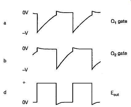
FIG15 Output waveforms of circuit of FIG14.
Because there is a small change in the forward gate bias on the conducting FET, following turn-on, the lower edge of the 'off' part of the waveform won’t be quite horizontal in profile. The duration of the 'on' and 'off' segments of the output waveform, at Z (the mark-to-space ratio), is largely determined by the time constants of R1C1 and R2C4, and the conducting characteristics of Q1 and Q2. If all components are accurately matched, this circuit will give a good 1:1 mark-to-space ratio, though there are better ways of achieving this aim.
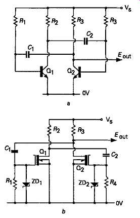
FIG16 Multivibrator layouts using bipolar and MOSFET transistors
This circuit can -- of course -- be built using both bipolar and MOSFET type transistors, using the modified layouts shown in FIGs 16a and 16b: a type of transposition which could equally well be done with any of the circuits described below, where I have chosen to illustrate the type of device which I think to be the most appropriate for the circuit chosen.
The source-coupled oscillator
This type of layout, shown in FIG17 as an arrangement based on MOSFETs, though it could also use junction FETs or bipolar transistors, is based on the long-tailed pair layout described in Section 6, and achieves free-running multivibrator action with the use of only one timing RC network.
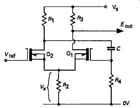
FIG17 Source-coupled oscillator
Its method of operation is that, if, because of an initial imbalance in the device characteristics, Q1 say, is driven towards cut-off by a voltage applied via C to its gate, the loss of Q1 source current through R2 will cause the voltage, V1, developed across R2, to decrease in relation to Vref, turning Q2 more fully on, with a consequent reduction in its gate potential -- which reinforces the action of switching off Q1: a process which is very rapid in effect. When the cut-off bias on Q1 decays away, and source current once more begins to flow through R2, the voltage V1 will begin to in crease, the current through Q2 will begin to decrease, and its drain voltage will become more positive, turning Q1 more fully on. Once again, this action is cumulative (sometimes called 'regenerative') in effect, so that this 'off' to 'on' transition is also very rapid.
The relaxation process is now one in which the gate and source voltages of Q1 decay back towards 0V, until the point is reached at which Q2 again begins to conduct, and the circuit switches back to its alternative state.
Because of its lower loop gain, the transition times for this circuit may not be quite as rapid as those of FIG14, but it offers the advantage that the output signal can be derived from the drain of Q1, an electrode which is not involved in the multivibrator action, so that the oscillatory frequency is not altered significantly by the nature of the output load impedance.
A more modern version of this kind of multivibrator is shown in FIG18, based on an opamp., Av In this the circuit is fundamentally unstable because of positive feedback through R2, from the output to the non-inverting input of A1, which means that the circuit will, on switch-on, rapidly assume a DC state in which the output is either as far positive as the circuit will allow, or as far negative. Current flow through R into C, connected to the inverting input, will then cause this point to become slightly more positive (or negative, as the case may be), which will cause the output voltage of the amplifier to switch into the opposite state, when the discharging, or charging, of C will begin again in an endlessly repetitive manner.
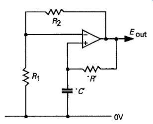
FIG18 Opamp astable circuit
This circuit will give an excellent symmetry in out put mark-to-space ratio, but the rapidity of transition from off to on states, and vice versa, will depend on the opamp. HF characteristics.
The 555 circuit
In view of the proliferation of application specific integrated circuits, it’s hardly surprising that ICs for use as free-running and triggered multivibrator circuits have been included in the range. Some of these circuits have survived for only a short period in the makers' catalogues before being superseded, but the '555' type device, in both bipolar and CMOS versions, has remained as a widely used component, used for both timing applications, and as a free-running oscillator, using the connection layout shown in FIG19.
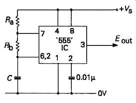
FIG19 Astable circuit based on 555 IC The on (1) and off (0) durations
of the output wave form, in its free-running state are given approximately
by…

The 'Bowes' multivibrator
A modification of the circuit of FIG17, variously attributed to both Bowes and White, in which the timing cycle is accomplished by the emitter circuit components, is shown in FIG20. (See Smith, J. H., El. Eng., p.426, Aug. 1963). Because of the low circuit impedances, and the fact that neither transistor is driven into saturation, this layout offers very rapid transition times.
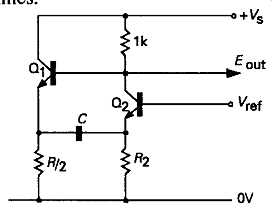
FIG20 The Bowes emitter coupled multivibrator
The 'Spany' pulse generator
This circuit (Spany, V. , EL Eng., Aug. 1961), shown in FIG21, employs a regenerative pair of transistors connected in series, so that either both devices or neither must conduct. This has the effect of generating a very brief output pulse, at a repetition rate determined by whichever of the two time-constant networks (C ^ or C^)» is the longer.
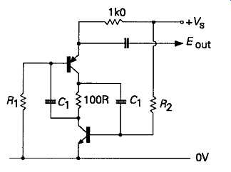
FIG21 The Spany pulse generator
The blocking oscillator
This arrangement, shown in FIG22, employs a pulse transformer (T1), connected so that an increase in current through the primary winding (P), causes a positive potential to be developed at the end of the secondary winding (S2), connected to the base of Q1 which will, in turn, cause an increase in the collector current passing through the primary winding of the transformer. The positive potential applied to the base of the transistor causes current to flow through S1 into C until the increase in base current can no longer be sustained by regenerative action. At this point, the current through P begins to decrease, and the potential at the base of Q1 begins to swing negative. To this potential is now added the accumulated negative charge acquired by C, which causes Q1 to be driven hard into cut-off.
The output waveforms which are given by this circuit are indicated in the diagram, and consist of a brief duration output spike from S2, and a large, and fairly linear, sawtooth waveform across C.
This circuit, in a valve operated version, enjoyed great popularity as a sawtooth generation system for use in picture frame scanning in television equipment.
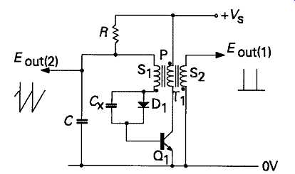
FIG. 22 Blocking oscillator circuit.
In the junction transistor operated version of the circuit shown in FIG22, a diode, D1, must be included in the transistor base lead, with perhaps a 'speed-up' capacitor connected across it, to prevent zener diode action in Q1 base -- emitter circuit limiting the possible negative swing on C.
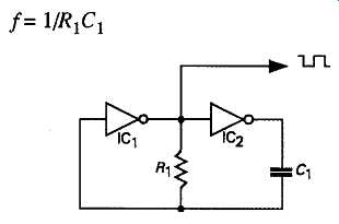
FIG23 Logic gate square-wave generator
Logic element based square-wave generators
Quite apart from the various digital IC types, usually described as 'flip flops', which can be con figured to operate as free-running multi-vibrators, there are two circuits, shown in FIGs 23 and 24, which are based on CMOS inverting buffers. The method of operation of the circuit of FIG 23 is that if the output of ICX is 'high', the output of IC2 will be 'low', and vice versa. This causes C1 to charge or discharge through R! until the potential at the junction of R1 and C1 reaches the threshold input potential of IC1, when the output of this amplifier will change state, and the cycle will repeat itself, giving a continuous rectangular-wave output waveform, of nearly 1:1 mark-to-space ratio, and a frequency of approximately:
f= 1/R1 x C1
The behavior of the circuit of FIG24 is very similar, except that a third inverting buffer, IC3, is connected as an active integration stage. If the output of IC2 is high, the output of IC3 will ramp downwards until, once again, the input threshold potential of IC1 is crossed, when the output of IC1 will go abruptly high, and the output of IC2 will make a very rapid negative transition -- reversing the input potential to IC3, and causing the cycle to start over again. This circuit gives a triangular waveform, from IC3 output, as well as a pair of complementary phase, nearly square, waveforms from IC1 and IC2 outputs.
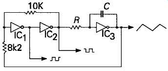
FIG 24 Square and triangular wave generator If an input sinewave is available,
CMOS inverting buffer amplifiers can be used to convert it into a nearly
symmetrical square-wave, having rapid rise and fall times, by the use
of the circuit shown in FIG25.
The resistor, R19 across Ax biases the amplifier into an input voltage setting which approximates to its DC mid-point, and assists in achieving the symmetry of the output waveform. Because a chain of three amplifier blocks is used, the final on/off transitions are rapid.
As with the circuit of FIG24, complementary phase output waveforms are available.
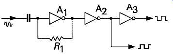
FIG 25 High speed squaring circuit
Sawtooth, triangular and staircase waveform generators
Several of the circuits shown above will generate triangular shaped output voltage waveforms which are useful for various circuit functions. However, the scanning of an oscilloscope, or TV tube, screen nearly always requires that the position of the spot shall move linearly across the screen, as a function of time, and this demands an input waveform which has a very linear relationship between output voltage and time.
In addition, it’s usually desirable that the voltage ramp is terminated by an abrupt flyback transition, in order that the ramp may begin again, giving a voltage/time relationship of the kind shown in FIG 26.
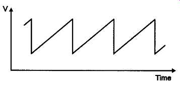
FIG 26 Oscilloscope X-axis scanning waveform
Three approaches are commonly employed for the purpose of generating a linear ramp waveform, of which the simplest is the use of a standard CR charging circuit, which is fed from a relatively high source voltage, as shown in FIG 27a, so that only the initial, and relatively linear portion of the exponential charging slope, seen as the potential across the capacitor, and shown in FIG 27b, need be employed.
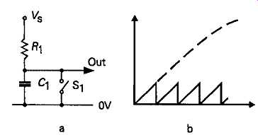
FIG 27 Simple sawtooth scan waveform generator circuit.
The second technique is to cause the timing capacitor (C1), to charge through a constant current source (CCS), as shown in FIG28a, so that the rate of change of voltage with time, shown in FIG28b, is constant, within the limits imposed by the constant current source, regardless of the proportion of the output waveform sampled.
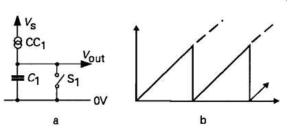
FIG 28 Improved sawtooth generator system.
The third method used it to connect the timing capacitor across a linear inverting DC amplifier, as shown in FIG 29. If the input current source, R1, is connected to a stable voltage reference point, the input current will remain virtually constant, as the output voltage ramps upwards or downwards -- which, in turn, will depend on the polarity of the input voltage reference -- since the action of the amplifier, if its gain is high enough, will be to generate a virtual earth node at its input, which, by definition, remains at a nearly constant potential.
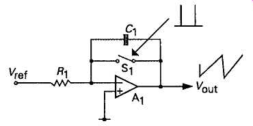
FIG 29 Negative feedback sawtooth generation circuit.
In all of these examples, the circuit will be reset by discharging the timing capacitor through some form of electronic switch, triggered repetitively by some externally applied trigger waveform. In most cases, it’s more useful if the reset function is triggered by the potential reached by the output voltage ramp, rather than just by some arbitrarily applied time interval.
In the case of the sawtooth circuit of FIG 29, the output waveform can be modified to that of triangular profile -- this term is usually employed to denote a waveform in which both linear slopes are of com parable duration -- by switching the input from a positive to a negative input reference potential. A practical example of such a waveform generator layout is shown in FIG 30.
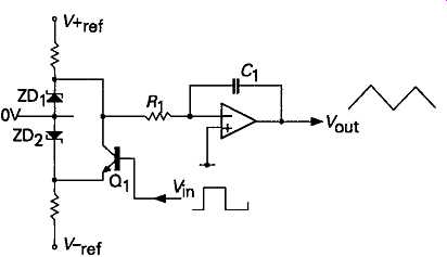
FIG30 Circuit allowing adjustable slope triangular waveform output
A type of waveform which has similar characteristics to the sawtooth is the staircase, shown in FIG 31. This type of waveform can be generated, as for example in the circuit layout of FIG 32, by introducing a uniform, unidirectional, sequence of pulses of charge into the input circuit of a high impedance integrating amplifier (A1). In the circuit shown, these pulses of input current are derived, from a charged capacitor (C1) by way of an electronic switch (S1) actuated by a square-wave control signal. The circuit can be reset by actuating S2, perhaps by means of an output ramp voltage level detecting circuit (A2). This approach is widely used, in a single or double ramp system, as a means of converting an input volt age level into a sequence of pulses, as, for example, in a pulse-counting type digital voltmeter.
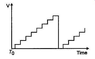
FIG31 Staircase waveform
Mark-to-space ratio adjustment
One of the useful purposes to which a triangular or double-ramp staircase waveform can be put is in the generation of rectangular waveforms in which the mark-to-space ratio can be adjusted by some externally applied control voltage. This can be done by using a triangular waveform as the input signal to a narrow input threshold amplifier, as shown in FIG 33. If the input reference voltage is adjusted, up or down, the slicing level of the amplifier will be modified, and the relative on and of f durations of the output rectangular wave will be altered.
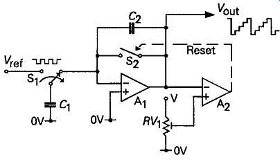
FIG 32 Staircase waveform generator circuit.
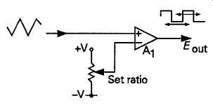
FIG33 Mark-to-space ratio adjustment.
In this application, the use of a double-ramp stair case waveform input will allow greater precision in the on and of f durations, which will be precisely synchronized to the leading edges of the initial ramp generating control square-wave, but at the cost of the loss of the potentially infinite variability of this ratio.
Negative impedance oscillators
These fall into two broad classes: those which employ a simple CR or LR timing circuit as the frequency determining element, and those which use an LC resonant circuit for this purpose. Of the first category, the simplest arrangement is that using a gas discharge device, such as a low pressure neon tube (Vn) in the type of circuit shown in FIG34. In this, when a suitable potential is applied to the free end of R1 the voltage across C1 will begin to climb exponentially towards the level of the applied input potential. Assuming that this is greater than the breakdown voltage of the gas discharge tube, at some point on the charging voltage ramp the tube will 'strike', and current from R1 and C1 will flow through the tube. At this point, the tube will exhibit a negative impedance, in that the greater the current flow, the lower the voltage across the tube -- because the conducting impedance of the tube is inversely proportional to the number of current carrying ions, and this increases as the discharge current increases.
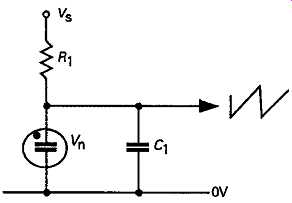
FIG 34 Gas discharge tube sawtooth oscillator.
Since the voltage drop across the tube will depend on the product of current flow and impedance, this negative impedance characteristic causes the output voltage to fall as C1 discharges through Vn> until the system reaches equilibrium, and no more current flows from Cv If R1 has a value which is relatively high in relation to the conductive impedance of the tube, when the current contribution from C1 ceases, the level of internal ionization in the tube will fall and its impedance will rise. However, because of the presence of C1, the voltage across the tube can only rise relatively slowly, and the conditions required for ionic conduction, at that voltage, are no longer met, and so the discharge will extinguish. This allows the voltage across C1 to rise, and the discharge sequence to repeat itself, giving a sawtooth output waveform, as shown.
A similar type of repetitive charge/discharge behavior will be given, though at lower applied voltages, by a range of modern semiconductor devices, such as the DIAC shown in FIG35, the uni-junction transistor of FIG36, and the silicon controlled switch shown in FIG37.
A more general category of negative impedance oscillator is that in which an LC tuned circuit, or other resonant system, is connected to an external negative impedance generator, such as For example the two stage feedback amplifier in the Franklin oscillator --see Section 12 -- or where the active agent is a tunnel diode, a device examined in Section 5, which has a voltage/current curve of the kind shown in FIG38. This type of device is notable for the fact that, for a significant range of applied voltage, any increase in applied potential will result in an reduction in device current -- a true negative impedance condition. When biased into this state, components such as this can be used, in principle, to make 'two-terminal' LC oscillator systems of the type shown in FIG 39. How ever, because of their relatively high cost, tunnel diodes are mainly used in VHF circuitry where other techniques are less conveniently applicable.
Devices such as the impatt diode, and the Gunn diode -- a highly doped three layer device, usually fabricated from gallium arsenide -- also exhibit negative impedance regions, parts of the voltage/current characteristics in which the current flow falls as the applied voltage is increased, and these are also used in low power oscillator systems, though almost exclusively as microwave signal sources.
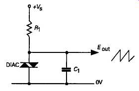
FIG 35 Relaxation oscillator based on DIAC
FIG 36 Sawtooth oscillator based on uni-junction transistor
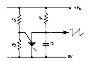
FIG 37 Relaxation oscillator using silicon controlled switch
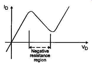
FIG 38 Tunnel diode current vs. voltage characteristics
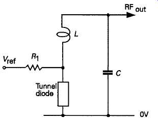
FIG 39 Tunnel diode negative resistance oscillator
Noise sources
'Noise' is generally regarded as an inconvenient, but unavoidable, accompaniment to all electronic signal sources and all subsequent amplification or manipulation processes, and care is usually taken, in the circuit design, to limit the proportion of the output signal which is due to noise -- as defined as a signal voltage of random occurrence and frequency distribution.
White and pink noise
For some types of test procedure it’s very useful to have a calibrated noise source. This type of signal generator will generally be a source of 'white' noise -- a term which is given to a noise signal which has the characteristic that the output power is constant for any equal unit of bandwidth. If converted into an audible signal, this kind of noise would have the sound of the hissing escape of gas from a high pressure system.
The type of noise known as 'pink' noise is that which has a constant output power for each octave of bandwidth, and in audible form, would sound like the rustling of leaves, or the sound of the wind through long grasses.
Since circuit elements designed to produce noise will generally have a white noise power distribution, within their useful bandwidth, some form of output filtering will be necessary to achieve the -3dB/octave reduction in voltage output, as a function of increasing frequency, required for pink noise characteristics. This can be done by an RC network of the kind shown in FIG. 40.
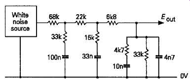
FIG. 40 Noise shaping circuit
Noise source systems and bandwidths
Several circuit layouts can be employed as wide-band noise sources, of which the simplest is the Edison diode, a directly heated filament, mounted in an evacuated envelope, in proximity to a positively charged metal anode, as shown in FIG41. Electrons will be emitted, and immediately collected by the metal plate, in a quite random manner, to give a noise (cur rent) output which is directly proportional to the square root of the measurement bandwidth and the anode current.
With suitable components, the type of circuit shown in FIG41 has a usable output over the frequency range 10Hz-1000MHz, a frequency at which inter electrode transit time effects and electron 'bunching' are beginning to impair the randomness of the output signal.
A commonly used alternative to the Edison diode as a noise source is the simple layout based on a gas FIG. 41 Noise diode circuit discharge tube shown in FIG. 42. In this the random collisions between the ionized atoms of gas in the space between the two electrodes give rise to a fluctuating output current which approximates to a true white noise source over the frequency range 100Hz-20kHz, which is adequate for audio purposes.
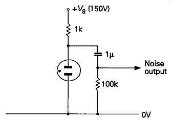
FIG 42 Gas discharge tube noise generator
A somewhat better performance is obtainable from a reverse biased avalanche diode (i.e. most zener diodes with a breakdown voltage above 5.5 V), used in the circuit shown in FIG 43. This is usable over the range 30Hz-100kHz. With a specially designed noise diode the bandwidth can be extended upward beyond 1GHz.
Comparable performance to that from an avalanche diode is given by the use of a silicon transistor base emitter junction which is biased into reverse break down, as shown in FIGs 44 and 45. The largest noise output is given at a bias voltage just greater than the base-emitter breakdown voltage, but this may exhibit random peaks in output voltage at unpredictable parts of the spectrum, so it’s prudent to choose an applied reverse voltage rather higher than this level, say, twice the breakdown value.
A further simple circuit is that based on a MOSFET input opamp such as the RCA CA3140, shown in FIG 46, which has a usable and fairly level noise voltage output over the range 10Hz-200kHz.
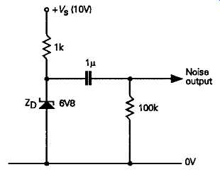
FIG 43 Zener diode noise source
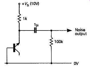
FIG 44 Reverse biased emitter-base junction noise source
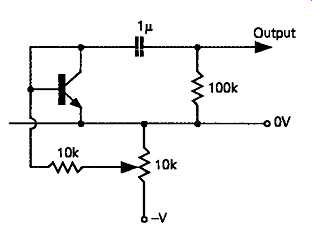
FIG 45 Junction reverse breakdown noise source
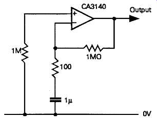
FIG 46 Opamp noise source