AMAZON multi-meters discounts AMAZON oscilloscope discounts
....cont. from part 1
Electronic meter systems:
The use of electronic amplification techniques provides an elegant means of increasing meter sensitivity, and minimizing any nonlinearities due to meter rectifier characteristics, as well as avoiding errors due to the presence of DC components in the signal being measured.
A typical AC voltmeter circuit based on an opamp and a moving coil meter/bridge rectifier combination is shown in FIG. 19. In this circuit arrangement, the fact that the meter/rectifier combination is placed in the feedback path of the amplifier means that the closed-loop negative feedback arrangement acts to generate a feedback voltage across R2 and C2 which is closely similar to the input voltage present across R1.
During those parts of the voltage swing across the meter/rectifier combination in which the silicon junction diode rectifiers are open circuit the negative feed back loop around the amplifier is disconnected, so that the amplifier output voltage (as seen at point '?') is driven, with the full opamp open-loop gain, to 'jump' across the rectifier open circuit voltage band, as shown in FIG. 20a. The voltage developed across R2 is as shown in FIG. 20b and that across the meter as shown in FIG. 20c.
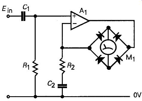
FIG. 19 Electronic AC voltmeter circuit
FIG. 20 Voltage waveforms in circuit of FIG. 19
Because there is no DC path through R2 and C2, the circuit will be insensitive to DC voltages present across Rh even were these not, in any case, blocked by C1. In this circuit, the meter FSD will be ImR2, where Im is the meter FSD current, so that, for example, if R2 = 100 ohms, and Im = 100µA, a full scale deflection of the meter would be given by a voltage of 10mV. The sensitivity of the circuit can be increased, as required, by increasing the overall AC stage gain of the circuit. The basic layout of such a multi-range AC millivoltmeter, is shown in FIG. 21. If the design specification for such an instrument was that it should have a bandwidth of 3Hz 1MHz, at its -3dB points, and a scale range of lmV-100V FSD, this order of bandwidth and sensitivity could be achieved with the basic meter/rectifier circuit without difficulty. However, there are problems which must be resolved in the design of the input attenuator, in respect of the desired input impedance (which should be high, to limit the error caused by connecting the meter to the circuit under test), and the (input open circuit) noise level at zero input signal, which is due to the thermal noise of the input attenuator resistors, and should obviously be as low as possible.
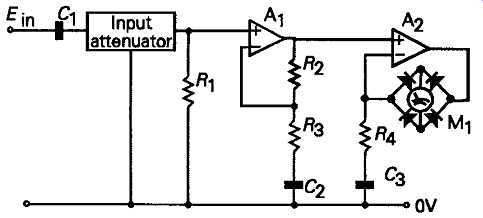
FIG. 21 Multi-range AC milli-voltmeter.
The designer has two options in this circuit, of which the first is to use a low resistance input circuit, such as the constant impedance attenuator network of the kind shown in FIG. 22, which offers an identical input and output resistance at all range settings, and however long the attenuator chain. In this kind of circuit layout, if K is the attenuation, Rt is the necessary value of resistance required to terminate the line, at both ends, and Rc is the required characteristic resistance of the attenuator (i.e. the value of resistance which will be seen by an ohmmeter between the 0V rail and any tapping point on the network), then the value of a will be given by
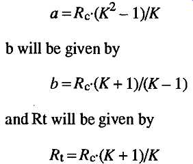
...so that if the desired attenuation from one step to the next was 10, and Rc -- the input impedance of the meter circuit -- is to be 10k-ohms, then a will be 99k, b will be 12.22k, and Rt will be 11.0k.
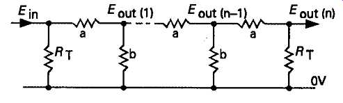
FIG. 22 Constant impedance attenuator network.
Assuming that this level of input resistance was acceptable in a general purpose multi-range instrument, and it’s somewhat on the low side, nevertheless it would still be associated with a background thermal noise voltage, over the 1MHz instrument bandwidth, of some 12µV. -- equivalent to just over 1% of the full-scale reading, which would cause a constant zero offset on all voltage ranges. This would probably be just about tolerable since the offset could be trimmed out by the meter zero adjustment, and the consequent scale error would not be great. On the other hand, increasing the characteristic resistance of the attenuator network to 100k, which would be more suitable for a general purpose instrument, would increase the background meter reading, due to thermal noise, to some 40.6µV, or 4% of FSD, and this would certainly not be acceptable.
Using the simple resistor chain attenuator arrangement shown in FIG. 23, in which the input resistance at the maximum sensitivity position was 1k, would reduce the zero-input-signal noise threshold to 4µV, or 0.4% of FSD, but this circuit layout would need some very high resistance values -- difficult to obtain with any precision -- for the 10V and 100V input ranges. Also, if it’s required that the basic HF -3dB response of the meter remains the same, regardless of the range setting, then care must be taken to keep the stray capacitances of the attenuator network as low as possible, so that their reactive impedances (Zc = 1/(2 pi fC)), are high in relation to that of the attenuator multiplier resistors. This would be feasible with the low impedance attenuator arrangement of FIG. 22, but not with that of FIG. 23.
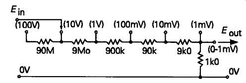
FIG. 23 Resistor chain attenuator circuit for 100V-lmVrange
A practical compromise, easily achieved with electronic meter systems, is to use an input attenuator to select the required FSD sensitivity over the ranges 1mV to 100mV, and then to adjust the gain of the amplifier feeding the meter/rectifier circuit to provide the 1-100V range settings, as shown in the final instrument design illustrated in FIG. 24. The only penalties with this arrangement are that on the 1mV FSD range, the meter will have a low (1k) input resistance and that the low frequency -3dB point is increased to 30Hz on this range. On all range settings above 100mV FSD the meter would accept an input voltage overload of up to 300V without damage. The variable resistor, RV1, is used, when the instrument is initially assembled, to set its FSD sensitivity to the required full-scale values, using an AC voltage reference standard.
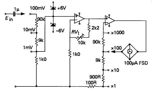
FIG. 24 Wide range milli-voltmeter with two stage attenuation.
Waveform distortion measurement
It’s often desirable that the waveform at the output of an AC signal processing or amplification system is the same as the waveform at the input. If the signal is non-sinusoidal, this kind of waveform distortion, when it’s present, can usually be seen on a cathode-ray oscilloscope display, provided that the change in waveform shape is big enough. However, even when the distortion can be seen, it may still be very difficult to define the effect in numerical terms.
With the rather more restricted category of sinusoidal (single tone) signals, a variety of techniques are available which can define, and quantify, the wave form distortions introduced by the system. These types of test may not be so informative about system defects or malfunctions, but are widely used simply because they do give numerical values by which the linearity of the system can be specified. These methods fall, generally, in two categories, 'notch filtering' and 'spectrum analysis'.
THD measurement by notch filtering:
This technique for measuring total harmonic distortion (THD) relies on the fact that a 'pure' sinusoidal signal will contain only the fundamental frequency, f0, free from any harmonics at 2f0, 3f0, and so on. If the signal under test is fed to a measuring system which has a notch in its frequency response, as shown in FIG. 25, and if this notch is sufficiently sharp that it will remove the signal at/0 completely, but give negligible attenuation at 2/0 and higher frequencies, then a measure of total harmonic distortion can be obtained by comparing the magnitude of the incoming signal, measured on a wide-bandwidth AC milli-voltmeter, in the absence of the notch, with that which remains after the fundamental frequency has been 'notched out'. There are a variety of circuit arrangements which can be used to provide a notch in the frequency response of an AC measuring instrument, such as the parallel tuned LC tuned circuit shown in FIG. 26a, the Wien nulling network shown in FIG. 26b, or the parallel-T notch network shown in FIG. 26c. Of these layouts, the tuned circuit would only be useful, in practice, at frequencies above some 50kHz. Below this frequency the size of the inductor would be inconveniently large. There could also be a problem of hum pick-up due to the inductor itself. Both the Wien and the parallel-T arrangements are practicable layouts for use in the 3Hz-100kHz range, though they will normally need to be somewhat rearranged to allow the use of negative feedback around the loop to sharpen up the frequency response of the system.
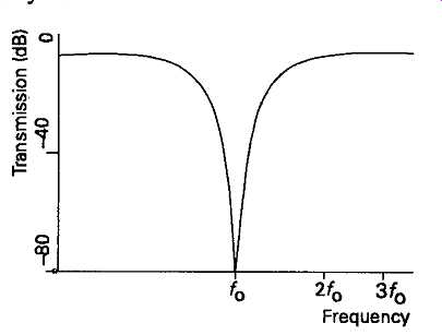
FIG. 25 Frequency response notch
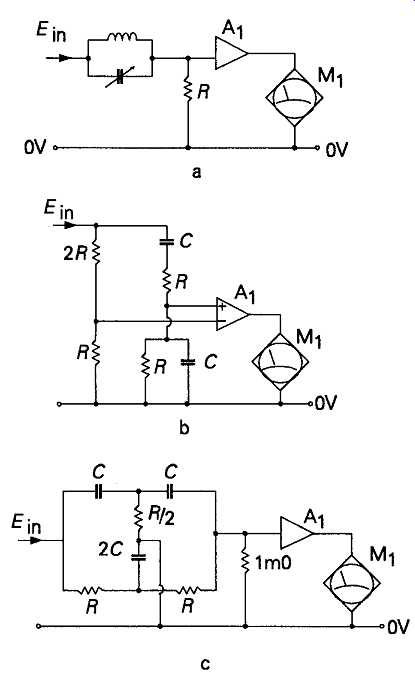
FIG. 26 Possible notch circuit arrangements
The principal advantage of the parallel-T notch net work is that it can be connected directly between the incoming signal and the measurement amplifier (e.g. an AC millivoltmeter) so that no additional noise or waveform distortion is introduced by any input buffering or amplifying stages. Two practical notch type distortion measuring systems of this kind, in which the sharpness of the notch is improved by the use of negative feedback around the notch-filter/amplifier loop, are shown in FIG. 27 and 28. These are capable, respectively, of measuring harmonic distortion residues as low as 0.008% and 0.0001% of the magnitude of the fundamental frequency, but this measurement of signal residues will also include any hum and noise voltages present on the input signal -- since these will still be left after the test signal, fo, has been removed by the notch circuit--and this snag often limits the sensitivity of the system.
The Wien network notch type of distortion meter is easier to use, on the bench, once the display sensitivity has been set, because it only requires two-knob adjustment (frequency tuning and bridge balance adjustment), whereas the parallel-T network generally requires three independent adjustments to achieve a precise null setting. If the signal being measured is at, say, 400Hz and above, reductions in the meter reading error, due to the presence of 50/60Hz and 100/120Hz mains hum, can be made by introducing a steep-cut high-pass filter, with a turnover frequency at, say, 400Hz, giving, perhaps, a -50dB (316x) attenuation at frequencies of 120Hz or lower.
Similarly, the error in the true THD reading due to the presence of the wide bandwidth white noise volt age present in the output can be reduced by restricting the measurement bandwidth by including a sharp cut off low-pass filter in the measurement circuit -- prefer ably with a switched choice of turnover frequencies, at, say, 10kHz, 20kHz, 50kHz and 100kHz.
Intermodulation (IM) distortion measurements:
One of the principle problems caused by nonlinearities in an amplifier transfer characteristic is that the magnitude of the output signal from such a circuit will vary according to whereabouts it sits on the transfer curve, as shown in an exaggerated form in FIG. 29. This effect is always present to some extent in any amplifier which has not got a ruler-straight input/output characteristic. In practice. This means that when two signals are present simultaneously -- let us assume that one is large and one is small -- the output voltage swing produced by the larger one will sweep the smaller up and down the transfer curve, modulating the amplitude of the smaller signal by so doing. This will lead to the generation of sum and difference output frequencies, so that if the two signals are f1 and f2 respectively, there will be present at the output, in addition f1 and f2, signals at f1+f2 and f1-f2. Putting some numbers to this effect, if two signals, at 60Hz and 5kHz, were introduced to a distorting amplifier, the resulting 60Hz modulated 5kHz output voltage will contain spurious frequency components at 4940Hz and 5060Hz. An IM distortion test based on signals at these frequencies, at a 4:1 amplitude ratio, has been recommended by the SMPTE (the USA Society of Motion Picture and Television Engineers).
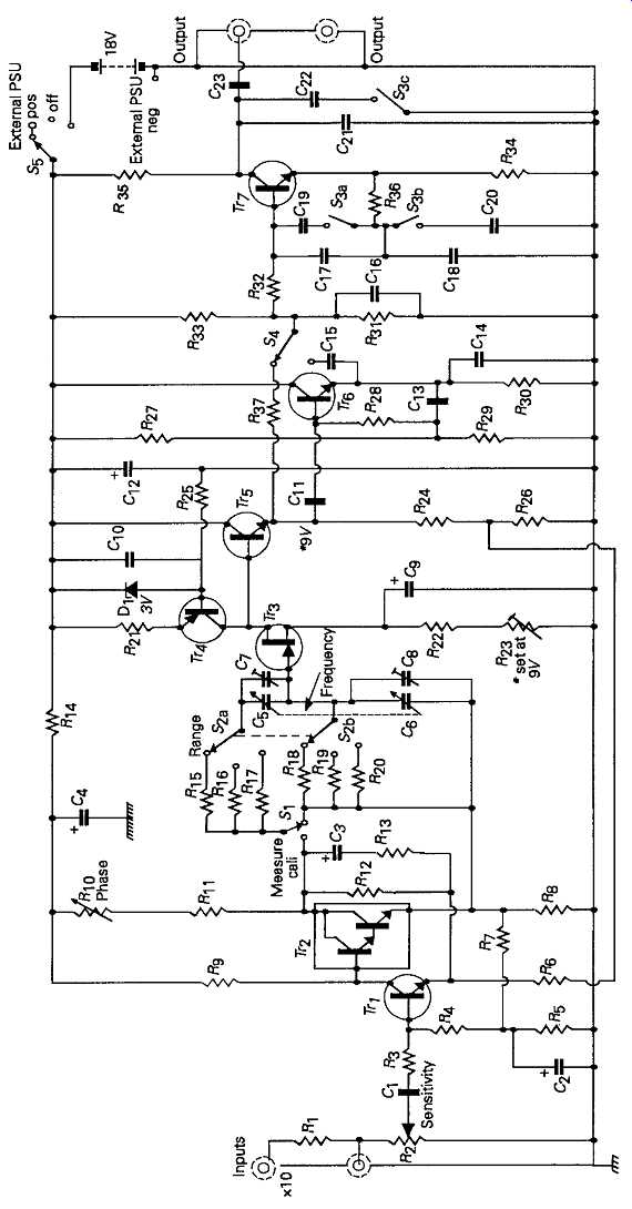
FIG. 27 Practical distortion meter based on Wien bridge notch arrangement.
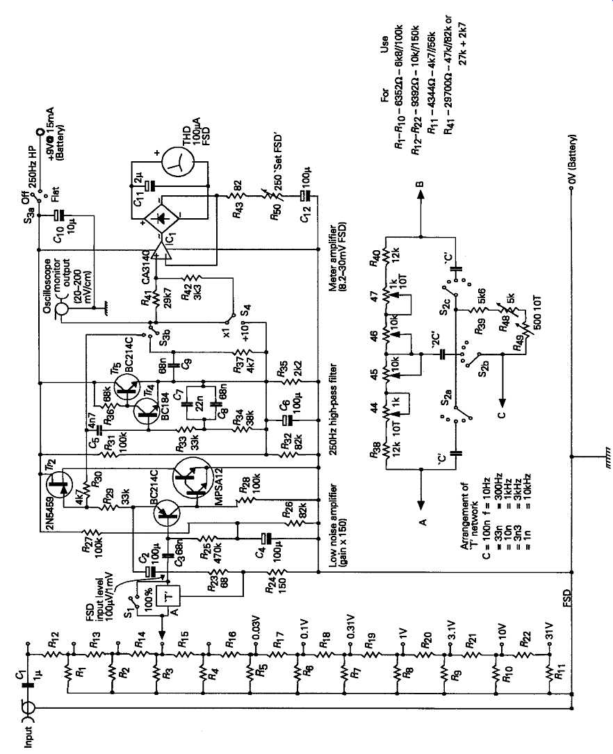
FIG. 28 Practical distortion meter circuit based on parallel T notch layout.
A practical measurement instrument for the SPMTE type test is shown, in outline, in FIG. 30. In this, the composite signals, after transmission through the system under test, are passed through a high-pass filter which removes the 60Hz component. The modulated 5kHz signal is then demodulated, which will result in the re-emergence of a 60Hz signal, and passed through a steep-cut low-pass filter to remove the 5kHz signal.
The magnitude of the residual 60Hz signal, as a pro portion of the 5kHz one, is then defined as the IM distortion figure.
An alternative IM distortion measuring technique has been proposed by the CCIF (the International Telephone Consultative Committee). In this procedure, the input test signal consists of two sine-waves, of equal magnitude, at relatively closely spaced frequencies, such as 9.5kHz and 10kHz, or 19kHz and 20kHz. If these are passed through a nonlinear system, sum and difference frequency IM products will, once again, be generated, which will result in spurious signals at 500Hz and 19.5kHz, or 1kHz and 39kHz, respectively, for the test signal frequencies proposed above. However, in this case, the measurement technique for determining the magnitude of the IM difference-frequency signal is quite simple, in that all that is needed is a steep cut low-pass filter which will remove the high frequency input test tones, and allow measurement of the low frequency spurious signal voltages. A suitable circuit layout is shown in FIG. 31.
In audio engineering practice, the value of IM testing, as, for example, in the case illustrated above, is that it allows a measurement of system nonlinearity at frequencies near the upper limit of the system pass band, where any harmonic distortion products would require the presence of frequency components beyond the pass-band of the system. Because these harmonics would be beyond the system pass-band they would not be reproduced, nor would they be seen by a simple THD meter, although the presence of nonlinearities would still result in the generation of spurious (and signal muddling) IM difference tones which were within the pass-band.
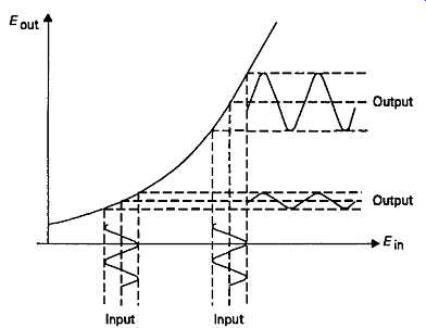
FIG. 29 Intermodulation distortion due to nonlinear amplification characteristics
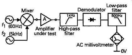
FIG. 30 The SMPTE intermodulation test arrangement
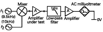
FIG. 31 The CCIF intermodulation distortion measurement procedure
Spectrum analysis:
The second common method of measuring harmonic and other waveform distortions is by sampling the output signal from the system under test by a metering system having a tunable frequency response, so that the measured output voltage will be proportional to the signal component over a range of individual output frequencies. The advantage of this technique is that if the system under test generates a series of harmonics of the fundamental frequency, but there is also an inconveniently large amount of mains hum and circuit noise, which would reduce the accuracy of reading of a simple notch-type THD meter, the relative amplitudes of the individual harmonics -- as well as hum voltages -- can be individually isolated and measured.
In use, the gain of the analyzer amplifier is adjusted to give a 100% (0dB) reading for the fundamental (input test signal) frequency, and the relative magnitudes of all the other output signal components are then read of f directly from the display. This type of analysis can also be used to reveal the presence of IM distortion products resulting from two or more input test tones.
The background noise level will depend on the narrowness of the frequency response of the frequency selective circuitry in the analyzer, and this will generally depend on the frequency sweep speed chosen, with a lower resolution for a fast traverse-speed oscilloscope display than for an output on a more slowly moving paper chart recorder.
Spectrum analyzers of this type are used at radio frequencies as 'panoramic analyzers', to show the presence and magnitudes of incoming radio signals in proximity to the chosen signal frequency, as well as for assessing the freedom from hum and spurious signal harmonics in an oscillator or amplifier design.
A typical circuit layout for a spectrum analyzer using the superhet system is shown, schematically, in FIG. 32. In this, the signal to be analyzed, and the output from a swept frequency local oscillator signal are separately fed to a low distortion mixer, typically using a diode ring modulator layout, and the composite sum and difference frequency signals are then amplified by an intermediate frequency gain stage, and converted into a unidirectional voltage by a logarithmic response detector circuit. If the frequency of the local oscillator is coupled to the sweep voltage which determines the position of the 'spot' on the horizontal trace of the oscilloscope, or the position of the pen on a paper chart recorder, there will then be a precise and reproducible relationship between measurement frequency and spot or pen position, so that the oscilloscope graticule or the recorder chart paper can then be calibrated in terms of signal magnitude and signal frequency.
Oscilloscope Linear, display 20kHz mixer 100 kHz Demodulator; 20kHz mixer; Input signal; Swept frequency oscillator; Time-base sweep voltage
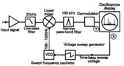
FIG. 32 analyzer
Schematic layout of spectrum:
A typical spectrum analyzer display for a high quality audio amplifier, showing mains hum components, as well as the test signal and its harmonics, is shown in FIG. 33.
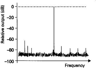
FIG. 33 Typical spectrum analyzer display
Transient distortion effects:
While the discussion above has been confined to the types of waveform distortions which will affect steady-state (i.e. sinusoidal) waveforms, for many circuit applications it’s important to know of the waveform changes which have occurred in 'step function' or rectangular wave signals, as illustrated in FIG. 34. Since these types of abrupt change in a pre-existing voltage level will imply, from Fourier analysis, an infinite series of harmonics (mainly odd order- such as 3rd, 5th, 7th and so on -- in square-wave or rectangular-wave signals), any signal handling system with less than an infinitely wide pass-band will result in a distortion of the input waveform. This may be just a rounding-of f of the leading edge of the signal waveform -- due to inadequate HF bandwidth, or 'overshoot' or 'ringing', as illustrated in FIG. 34, due to the introduction of spurious high frequency components, or just due to errors in the relative phase of the composite signal harmonics.
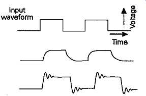
FIG. 34 Typical transient distortion effects.
It’s difficult to derive numerical values, from simple instrumentation, which relate to the nature of any of these rectangular waveform signals, except 'rise time', overshoot magnitude, 'settling time' -- to some specified accuracy level -- or slewing rate (the maximum available rise-time, where this is limited by some aspect of the internal system design), characteristics also shown in FIG. 35. These effects are most easily seen on an oscilloscope display, and if it has calibrated X and ‘Y' axis graticules, their magnitudes in time or voltage, may be approximately established.
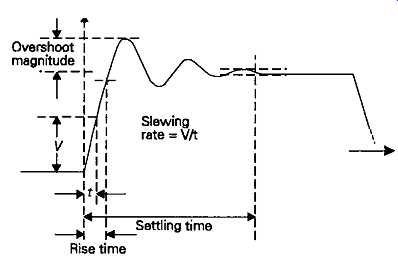
FIG. 35 Quantifiable transient response characteristics.
Oscilloscopes:
The oscilloscope is one of the most useful and versatile analytical and test instruments available to the electronics engineer. Instruments of this type are available in a wide range of specifications, and at a similarly wide range of purchase prices.
In its most basic form, this type of instrument consists of a cathode ray tube in which the electrons emitted by the heated cathode are focused onto the screen to form a small point of light, and the position of this 'spot' can be moved, in the vertical, 'Y-axis', and horizontal, 'X-axis', directions, by deflection volt ages applied to a group of four 'deflection plates' mounted within the body of the cathode ray tube. In normal use, the plates controlling the horizontal movement of the spot are fed with a voltage derived from a linear sawtooth waveform generator, giving an output voltage, as a function of time, which is of the kind shown in FIG. 36. The effect of this is to allow signals displayed in the vertical, Y axis, to be seen in a time sequence. A range of sawtooth waveform repetition frequencies is normally provided, giving a range of deflection speeds, which will provide cm/s, cm/ms, or cm/ps, calibrations.
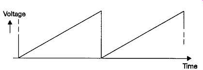
FIG. 36 Output sweep voltage applied to oscilloscope X-deflection plates
--- Time:
The X deflection (time-base) scan speeds are con trolled by a range switch, allowing a switched choice in a 1:3:10:30:100:300, type of sequence, but it’s also necessary for there to be a variable time-base scan speed control to allow the choice of intermediate values between these set choices of time-base frequency.
An important feature of any time-base sweep generator system is that it should allow the X scan to be synchronized with the periodicity of the signal to be displayed, where this is repetitive, so that the wave form pattern will appear to be stationary along the X axis. The more versatile and effective this synchronization facility is, the easier it will be to use the scope.
A typical time-base sweep voltage generator circuit is shown, schematically in FIG. 37. It’s normal practice in better quality instruments to provide both a time-base sawtooth waveform output, for the control of other instruments, such as spectrum analyzers or frequency modulated oscillators (wobbulators), and also a time-base switch position -- sometimes designated 'XY' -- which will allow the injection of an external signal into the X amplifier circuit. This facility will allow the oscilloscope to be used for measurements such as the relative phase of two synchronous waveforms, and also for determining the repetition frequency of an unknown signal, by means of 'Lissajous figures', of which some simple patterns are shown in FIG. 38.
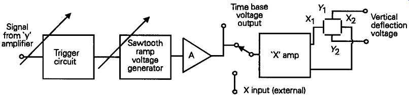
FIG. 37 Schematic layout of time-base generator circuit ---[ Signal from
? T* amplifier / Trigger circuit /sawtooth A ramp voltage; Time base voltage
g output generator Vertical L- deflection 1 voltage ]
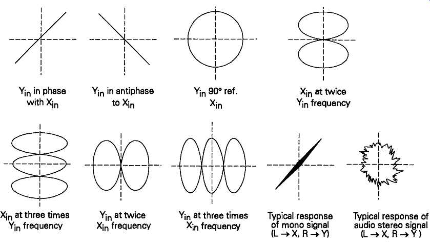
FIG. 38 Typical Lissajous figures
A separate signal input to a low distortion wide bandwidth voltage gain stage provides the vertical,' Y' axis, deflection of the oscilloscope 'trace'. In most modern instruments this will be a DC amplifier design, but with a switched capacitor in series with the input circuit to allow the DC component of an input compo site signal to be blocked. This would be essential in cases where the presence of a DC offset voltage would otherwise prevent the full range of amplifier gain being used, such as when it was desired to examine a relatively low magnitude AC signal present at the same time.
Typical amplifier specifications offer gain/frequency characteristics which are substantially flat from DC to perhaps 10, 20,50, or 100MHz, with some specialist scopes giving upper -3dB turn-over frequencies as high as the GHz range. In the lower bandwidth designs, preset switched input sensitivity values ranging from 1mV/cm to, perhaps, 300V/cm are offered.
Multiple trace displays:
The enormous usefulness of being able to display two or more signals, simultaneously, so that one could, for example, with a dual trace instrument, look at the input and output waveforms from a signal handling stage, has made multiple beam scopes much more common. The early twin-beam oscilloscopes used a cathode ray tube which had two entirely separate electron gun, focus and' Y deflection assemblies, so that the incoming X axis signals could be displayed entirely independently. However, this type of tube is both expensive and bulky, so that, in modern instruments, a single gun tube is used, and the time base trace is split, electronically, into two or more separate scans, by applying a rectangular waveform voltage signal to the input of the final stage of the deflection amplifier. The same signal is also applied to an electronic switch between the outputs of the amplifiers and the output display driver stage. A schematic layout for this type of multiple trace display system is shown in FIG. 39.
What happens, in practice, at higher scan frequencies, is that, for a time interval corresponding to the duration of a single 'Y' axis sweep, a vertical deflection voltage derived from, say, the G front panel shift control, combined with the output from the Y amplifier itself, are switched to the Y axis output voltage amplifier and deflection plates. During the next X axis sweep, a vertical deflection voltage from the front panel 'Y2' vertical shift control, and the output from the amplifier, are switched to the display system, but the outputs from the amplifier and shift controls are disconnected. Similarly, if there are input circuits, these will also be used to display their outputs on successive time-base sweeps.
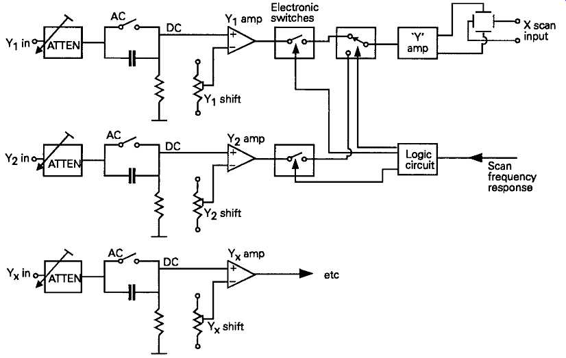
FIG. 39
Because of the persistence of vision, at higher time base speeds, the successive appearances of signals from the various Y inputs will be merged in the perception of the viewer, and will seem to be present simultaneously. Moreover, since the vertical shift volt ages are also switched, it’s possible to move the sequential Y displays, independently, on the scope screen, exactly as if there were a number of completely independent gun and deflection assemblies within the tube.
At lower sweep frequencies, where the limited persistence of vision would no longer allow a flicker free display, it’s normal practice to switch the amplifier outputs and shift voltages at a some high multiple of the scan frequency, so that, if the resolution of each trace were high enough for it to be seen, each trace would consist of a sequence of closely spaced dots.
Storage oscilloscopes:
The normal 'real-time' oscilloscope is only able to display the character of a signal, in a given volt age/time sequence, at the moment it happens, and only then if it’s accurately repetitive -- so that each successive X direction scan repeats and reinforces its predecessors. However, there are instances where the signal which is of interest is sporadic or randomly occurring, and it’s wished to examine in detail this particular event, recorded, briefly perhaps, on an externally triggered trace.
In early 'scopes, the only available technique was to use a 'long-persistence' screen phosphor, so that the image of the trace would only fade away fairly slowly.
An improvement on this system is to use a type of 'scope design in which one layer of a two layer screen is coated with a phosphor which has a fluorescence threshold somewhat above the energy level provided by the 'writing' beam. The image of the last scan pattern can then be recovered by flooding the screen with electrons from a so-called 'flood' electron gun, and this image will persist, at high brilliance, until the flood gun is switched off, and normal writing continues.
However a whole new family of 'scopes has arisen, to make use of the ability of fast analogue to digital (A-D) converters and high storage capacity digital memory techniques to store and recover digitally en coded signals. Using this technique, an incoming ?' axis voltage signal is sampled, at a repetition frequency high enough to give, say, 500 or more voltage sampling points across the X axis scan. This series of discrete signal voltage levels can be stored in random access memory (RAM), cells, from which the digital information can be recovered in its proper time sequence, and decoded, once more, by a digital to analogue. (D-A), converter, to generate an accurate replica of the signal present on the scope at the time when the signal was stored.
The great advantage which this technique offers, by comparison with long-persistence phosphors, or flood gun systems, is that, depending on the resolution of the stored signal -- which depends on the number of volt age sampling points, in the Y axis provided by the A-D and D-A converters, and on the number of time sampling points in the X axis -- the recovered signal can be examined in greater detail by expanding various points of the vertical and horizontal image scale. Although the shape of the signal will be preserved, the time axis is now an arbitrary one, reconstructed from pulses derived from the system clock.
Markers indicating the voltage and time characteristics of the original waveform may be superimposed on the recovered signal to simulate the characteristics of a real-time signal.
A schematic layout of a digital storage oscilloscope system is shown in FIG. 40.
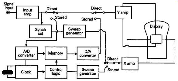
FIG. 40 Schematic layout of digital storage oscilloscope
Frequency measurement:
Although an approximate indication of signal frequency can be obtained from a Lissajous figure, on an oscilloscope display, this is an awkward measurement to make, and is usually time consuming. For high frequencies, the standby of the 'amateur' transmitter enthusiast was the 'grid dip' meter, or its transistorized variants, such as that shown in FIG. 41. In this, the current drawn from the power supply by a low power oscillator is reduced when the oscillator frequency is adjusted to coincide with that of the unknown signal, when this signal is inductively are capacitatively coupled to the dip-meter oscillator coil.
This, also, is only as accurate as the calibration of the dip-meter tuned circuit.
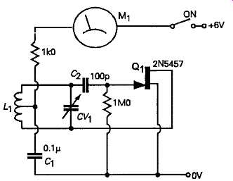
FIG. 41 Grid dip frequency meter.
A much better system, and one which is now almost universally used, is the digital display 'frequency counter'. This operates in the way shown, schematically, in FIG. 42. In this, the incoming signal, after 'conditioning' to convert it into a clean rectangular pattern pulse train, of adequate amplitude, is passed through an electronic switch (gating) circuit, which feeds those pulses received during a precise time interval on to a digital pulse counter system. For convenience in use, the final count is switched to the display through a storage register, to allow the counter to be reset between each measurement interval. The accuracy obtainable is determined by the precision of the setting of the frequency of the crystal oscillator which controls the timing cycle, and by the number of pulses which are allowed through the gating switch, which, in turn, depends on the input frequency. At 1MHz, a gate duration of 0.01 seconds would allow an accuracy of one part in ten thousand, but at 1000Hz, a gating interval, and display refresh periodicity, of once every ten seconds would be needed to achieve the same accuracy.
For high precision frequency measurements where very protracted counting periods would otherwise be necessary, 'frequency difference' meters are usually employed. In these instruments, the difference between the incoming signal frequency, and that of a heterodyne signal derived from an accurate reference frequency is determined. This technique allows accurate frequency measurements to be made in greatly reduced time intervals.
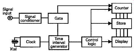
FIG. 42 Schematic layout of frequency counter
Signal generators:
The majority of the tests carried out on AC amplifying or signal manipulation circuits require the use of some standardized input signal, in order to determine the waveform shape or amplitude changes brought about by the circuit under test. These input signals are derived from laboratory 'signal generators', and these are available in a range of forms. In low frequency sinewave generators, the major requirements are usually stability of frequency, purity of waveform, and freedom from output amplitude 'bounce', on changes of frequency setting, with the accuracy of frequency or output voltage being relatively less important.
In HF and RF signal generators, precision and stability in the output frequency are essential, as is usually the accuracy of calibration of the output volt age -- particularly where the instrument is to be used to determine receiver sensitivity or signal to noise ratio. The purity of the output waveform is usually less important provided that the magnitudes of the output signal harmonics, or other spurious signals, are sufficiently small.
RF signal generators usually make provision for amplitude modulation of the signal, either by an internal oscillator or by an external signal source. This facility is useful to determine the performance and linearity of the demodulator circuit of RF receivers, and may also be helpful in aligning RF tuned circuits.
Other test signals, of square-wave or triangular waveform, are also valuable for test purposes, and these are usually synthesized by specialized waveform generator ICs, and available as wide frequency range 'function generators'. These offer square and triangular output waveforms, as well as a sinewave signal of moderate purity, usually in the range 0.1-0.5% THD. They do have the advantage that they allow a rapid frequency sweep to be made, to check the uniformity of frequency response of the circuit under test.
Beat-frequency oscillators:
These instruments derive a relatively high purity, wide frequency range, output signal by heterodyning two internally generated RF signals, as shown in FIG. 43, and then filtering the output from the mixer stage so that only the difference frequency remains.
The major drawback of this technique is that any relative instability in the frequency of either of the RF signals, from which the heterodyne output signal is derived, will be proportionately greater in the resulting difference frequency signal.
Output:
FIG. 43 Layout of high frequency BFO (see FIG. 11)
Frequency modulated oscillators (wobbulators)
These types of signal generators are almost exclusively used in RF applications, such as in determining the transmission characteristics of the tuned circuits or filter systems which define the selectivity of the receiver, and in aligning these receivers. If the linearity of the modulation characteristics of the oscillator are high enough, it will also allow the distortion characteristics of an FM receiver or demodulator to be measured.
Prev. ------- Next