AMAZON multi-meters discounts AMAZON oscilloscope discounts
It’s probably reasonable to assume that most people reading this guide will want to build some of their own projects, whether from plans in a magazine or book, from their own design, or from a kit. In any of these cases, you will need to know some thing about construction techniques. This knowledge is even needed for many commercial kits that have rather brief instructions that assume you know what you’re doing. (A notable exception was the Heath Company. Their manuals are generally excellent, leading the first-time project builder step by step through the construction process without really talking down to the old-hand electronics hobbyist.)
Obviously, constructing a circuit involves more than just gathering the components together and tossing them into a box. Some sort of electrical connection must be made between the component leads, according to the pattern of the schematic diagram. There are several popular types of construction in wide use today. These methods are briefly discussed in this section.
Start with the construction technique known as breadboarding, which is the one best-suited methods for the experiments in the next section (and in sections 23 and 31). It’s strongly recommended that you perform each of the experiments yourself. You will learn more this way than if you just read about them.
Breadboarding
Breadboarding is a method of temporarily hooking up electronic circuits for testing and experimenting. Of course, you could hard wire (connect components with wire and solder) each test circuit, as if it were intended for permanent use. But hard wiring can rapidly become extremely expensive.
You could cut costs somewhat by desoldering each circuit when you’re through with it and reuse the components. But desoldering tends to be very tedious, time consuming, and quite inconvenient. Besides, the repeated heating and reheating of component leads can damage some components.
Fortunately, there is a much more convenient device that allows you to set up temporary circuits—the breadboard. In its simplest form, this is merely a solderless socket that the various component leads and wires can quickly be plugged into or pulled out of. A typical solderless socket is shown in FIG. 1. The various holes in this type of socket are electrically connected to each other. The most frequently used pattern is shown in FIG. 2.
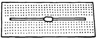
FIG. -1 A typical solderless socket.
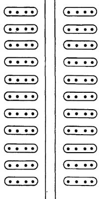
FIG. -2 The most commonly used interconnection pattern for a solderless
socket.
These sockets can make experimentation and circuit design much easier, but they are even more useful as part of a complete breadboarding system. These systems consist of a solderless socket and various commonly used subcircuits, such as power supplies (which produce a desired dc voltage from the standard ac house cur rent, thus saving battery costs) and oscillators (which produce an ac signal, usually with a variable frequency). These subcircuits can be separate, self-standing units used along with a simple solderless socket, but it’s generally more convenient to have them grouped together within a single, compact unit. At any rate, these subcircuits will be needed far too often to make breadboarding them each time they’re needed reasonable. The way these (and other) basic circuits work is described in detail in other sections.
If you don’t have a power supply available, you can perform the experiments in the next section with dry-cell batteries. There will be no difference in circuit operation.
Unfortunately, there is really no substitute for the variable-frequency oscillator. If you don’t have such a device, you won’t be able to perform Experiments 7 through 9. Just read these experiments carefully for now. I in this book, you’ll learn how to build an oscillator. Once you have learned this, you can return to section 16 and complete these experiments.
You should have no problem performing the rest of the experiments in section 16.
Finally, most breadboarding systems have one or more potentiometers and switches handily available for use in experimental circuits.
Once you have designed your circuit, bread-boarded the project, and gotten all the bugs out (bugs are errors that prevent your project from working properly), you will probably want to rebuild some circuits in a more permanent way. Solderless breadboarding sockets are great for testing and experimenting with prototype circuits, but they really aren’t much good when it comes to putting the circuit to practical use. Breadboarded circuits, by definition, have nonpermanent connections. In actual use, some component leads will easily bend and touch each other, creating potentially harmful short circuits. Components can even fall out of the socket altogether when the device is moved about. Interference signals can easily be generated or picked up by the exposed wiring.
Generally, packaging a circuit built on a solderless socket will be tricky at best. They tend not to fit well in standard circuit housings and boxes. Also, a solderless socket is relatively expensive. It’s certainly worth the price if it’s repeatedly reused for many different circuits. But if you tie it up with a single permanent circuit, you are only cheating yourself. Less expensive construction methods are available that are more reliable, more compact, and offer better overall performance.
Soldering
Most permanent circuit construction methods involve soldering. When soldering, you melt a special metal (called solder) over the connection point of two or more leads, binding the leads together and creating a strong, reliable mechanical and electrical connection.
There are different types of solder available for various purpose Some of these are summarized in Table 15-1. The most common type used in modern electronics work is 60-40 solder. This type of solder is composed of 60% tin and 40% lead. It has a rosin core. For electronics work, you must use rosin-core solder only. Never use acid core solder on any electronic circuit. The acid is highly corrosive and will eat through many of the components. Acid-core solder is used only for metal bonding applications.
----Table 1. T types of solder.
Metal used Core Melting point °F ,°C Applications
* TL indicates tin-lead alloy. Percent of each metal in the alloy is shown by the numbers.
Some solder is sold with no core at all. It’s used with a separately applied rosin paste. The rosin helps make a good electrical connection between the leads being soldered together.
Before soldering, clean the leads. A few quick rubs with some fine sandpaper will be sufficient in most cases. Arrange the leads in a mechanically solid connection before soldering. If the mechanical connection is weak, you will most certainly end up with a poor solder joint.
For most modern electronics work, you should use a low-power soldering iron. Generally a 20 to 30W unit will be best. Many electronic components are very sensitive to heat. Semiconductors (discussed in other sections) are especially sensitive. Even with a low-power soldering iron, don’t apply heat near sensitive components for too long a time, or you will damage them.
Don’t use a high-power soldering iron or soldering gun. Most low-power soldering irons are shaped like the one shown in FIG. 3. This type of iron is some times called a soldering pencil. You can also find some low-power soldering guns with an easy-to-hold, pistol-like handle.
Better soldering irons are grounded. Grounding reduces problems with static electricity, which can damage some electronic components, especially CMOS (complementary metal-oxide semiconductor) ICs (integrated circuits). (See section 28 for more information). A grounded soldering iron usually isn’t absolutely necessary, but it’s desirable.
Warm the soldering iron fully before you begin soldering. For most soldering irons, this means you need to plug it in for about 5 to 10 minutes before you actually start soldering. For maximum safety, place the hot soldering iron in a soldering iron stand when not actually being used. A typical soldering iron stand is shown in FIG. 4. You can buy such stands for just a few dollars, and they can reduce consider ably the potential hazards of accidental burns to your body or fire. They are very cheap insurance. Don’t scrimp on safety
FIG. -4 A soldering iron stand can reduce the risk of burns or fire.
Clean the soldering iron tip periodically on a damp sponge. If too much rosin and miscellaneous build-up accumulates on the tip of the soldering iron, the heat transfer will be significantly reduced. The odds of producing cold solder joints (explained below) will increase enormously.
FIG. -3 Most low-power soldering irons use the pencil shape. Insulated handle; Tip; Power cord
Before actually soldering, tin the tip of the soldering iron; melt a little bit of solder (not too much) over the tip. Use just enough to coat the tip with solder.
Good soldering is normally a two-handed process. (Some specialized soldering aids will let you solder one-handed, but this is by far the exception, rather than the rule.) Hold the handle of the soldering iron in one hand and the solder in the other. Apply both to the joint being soldered as shown in FIG. 5. Don’t apply the iron directly to the solder as shown in FIG. 6. You don’t want to melt the solder and let it drip over the joint. The idea is to heat up the joint so that the solder will flow evenly over it.
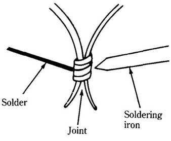
FIG. -5 Apply heat and solder separately to the joint.
FIG. -6 Don’t apply the soldering iron directly to the solder.
Make the solder joint as quickly as possible, remove the unused solder and the soldering iron from the joint without moving or jarring the joint before the melted solder has a chance to cool and set. It takes a couple seconds for solder to set. If you move the joint before the solder hardens, you will likely wind up with a cold solder joint.
Cold solder joints are one of the most common causes of problems in newly built electronic circuits, especially those built by beginners. Examine all solder joints very carefully. A small, high intensity lamp and a magnifying glass can be very helpful. A good solder joint will look smooth and shiny. If any solder joints look rough or grainy, they are probably cold solder joints. The cure is simple enough—just reheat the connection to re-melt the solder and let if flow more smoothly over the joint. In a cold solder joint, there is not a good electrical connection between the soldered leads. In some cases, the mechanical connection is pretty weak too.
The term cold solder joint really refers to a number of possible problems. One of the easiest to visualize is a bubble within the solder joint. This kind of problem is shown in FIG. 7. From the outside, the leads appear to be soldered together, but they aren’t.
Cold solder joints are not always apparent when you examine the joint. Even an experienced expert won’t be able to identify all cold solder joints. If the completed project does not work properly, a cold solder joint might be the problem. Sometimes, if the project is not too complex, it’s worthwhile just to reheat all of the solder connections rather than fry to track down the specific trouble spot.
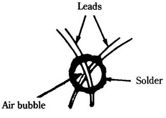
FIG. -7 A cold solder joint could be the result of an air bubble. Solder;
Air bubble
When soldering, be very careful not to create any solder bridges. A solder bridge is an undesired connection made by excess solder between two connections or adjacent printed circuit traces. Solder bridges are most likely to be a problem when a printed circuit board (discussed in this section) is used. Integrated circuits (or ICs), with their closely spaced pins are also frequent candidates for solder bridges. ICs will be discussed in other sections. A careful examination of all solder joints can help save you a lot of grief. Check for solder bridges after each connection is made. Then when all soldering is complete, go back and carefully re-examine all the solder joints again before applying power to the circuit. Remember, a solder bridge is a form of short circuit, if a power line or a signal gets into the wrong part of the circuit, the circuit won’t work properly, and, in some cases, some components (usually the more expensive ones) can be damaged or destroyed.
Don’t use too much solder. Use enough to cover the joint thoroughly, but don’t fill your project with great, ugly lumps of solder. In addition to looking unattractive and unprofessional, too much solder can be the source of many problems. The more solder you use, the greater the chances of solder bridges, and the greater the likelihood that it all won’t melt thoroughly, and cold solder joints will result. If you use too much solder, you will have to apply more heat longer to each joint, increasing the chances of damaging delicate semiconductors. Use what you need, but don’t resort to overkill.
Desoldering
if you work in electronics (whether professionally or as a hobby), sooner or later you’re going to have to do some desoldering. Desoldering is not the fun part of electronics. It’s not awful, but it tends to be a tedious and obnoxious task at best. There are probably no electronics technicians or hobbyists who say they enjoy de soldering. It’s sometimes necessary, and it can save you a lot of money. Desoldering is just the opposite of soldering, as the name suggests. The joint is heated and the solder is removed. This action permits you to remove and replace a component in the circuit.
Suppose you make a mistake and solder the wrong two leads together, or per haps you happened to get a bad component. Perhaps, a project or other circuit has been in use for a while, and you’d now like to modify the circuit in some way. In any of these instances, desoldering is the only alternative to junking the whole thing and starting over from scratch, which not only an extremely inelegant solution, it tends to be ridiculously expensive.
The tricky part of desoldering is removing the old solder. Don’t be deceived by advertising claims, no device is going to make desoldering truly easy or convenient. Some devices make the job a little less of a chore, but it’s still something you’ll want to avoid as much as possible. Aside from the sheer nuisance value, desoldering can overheat temperature-sensitive components (especially semiconductors). Desoldering almost always takes longer than soldering. Basically, there are two main approaches to removing old solder in a desoldering operation:
-Capillary action
-Suction
Each of these methods are discussed below.
Capillary action:
The capillary action approach to desoldering uses a braided cable. You press this cable against the joint as the solder is reheated. Thanks to some principles of physics (which you don’t need to go into here), the melted solder will be drawn up into the braid. This effect is known as capillary action.
Desoldering braid is available from many electronics dealers, including the ever-present Radio Shack chain. Unfortunately, some people seem to have a lot of difficulty with this method. They can never seem to get enough solder sucked up by the braid. Others find the capillary-action method such a snap, they use ordinary stranded wire in place of the special desoldering braid.
If you can get capillary action to work for you, it tends to be the most efficient method. But, if after numerous tries you can’t get it to work, don’t get too upset. You’re not alone. It seems to be a specialized skill that some people have a natural knack for, and others don’t.
Suction:
Melted solder can also be removed with suction. Some sort of vacuum device pulls the molten solder up into some type of container. Almost anybody can use these suction devices, but generally, they are not quite as efficient as desoldering braid. A good suction device can be fairly expensive. They often tend to spit out tiny globules of solder that can cause short circuits if you are not careful. They are also prone to clogging when portions of sucked-up solder harden in the intake nozzle. The simplest and least expensive suction based desoldering devices are simple rubber bulbs with a nonstick nozzle. Such a device is shown in FIG. 8.
To use the bulb, squeeze and hold it, forcing most of the air out of it. Bring the nozzle into position over the melted solder, and release the bulb. There is now a minor vacuum within the bulb, because of the expelled air. Nature abhors a vacuum, so a strong suction force will appear at the nozzle until the pressure outside and inside the bulb is equalized. (This just takes a fraction of a second.) If the nozzle is properly positioned over molten solder, the liquid solder will be pulled up into the bulb. You will usually need several repetitions of this process to remove a sufficient amount of solder from the joint to allow removal of the component.
FIG. -8 A simple rubber bulb with a nonstick nozzle can be used for desoldering. Rubber or plastic squeeze bulb.
The next step up in suction-based desoldering devices uses a spring loaded piston. In the set-up position, the spring is compressed, and a plastic plug blocks the nozzle. Some sort of triggering mechanism is included on the device. When the trigger is activated, the spring is released, and the plug/piston is pulled quickly back out of the way, creating a momentary vacuum and suction force. Again, the liquefied solder is pulled up into the nozzle. There are many variations on this type of device. Some work a lot better than others, of course.
If you frequently have to do a lot of desoldering, you might want to purchase an electric desoldering pump. These rather expensive devices work in a manner very similar to the common vacuum cleaner.
Point-to-point wiring
Now, read about some actual permanent construction techniques for electronic circuits. For fairly simple circuits using just a handful of components, you could use point-to-point wiring. No real base for the components is used. The leads of the components are simply soldered together. Often solder terminals are used. A solder terminal is a strip of Bakelite or other plastic with a screw-down foot for mounting onto the case of the project. One or more metal loops are provided as connection points for the leads to be soldered. Some typical solder terminals are shown in FIG. 9. The leads to be soldered are mechanically connected to the metal loop, or terminal, as shown in FIG. 10. The connection is then soldered.
This construction method is only suitable for very simple circuits. For a circuit of any complexity, you can very easily run into problems with “rats nest” wiring. Rats nest is a fairly self-explanatory name for jumbled wiring that goes every which way, full of tangles. Such jumbled wiring is next to impossible to trace if any error is made or if the circuit needs to be serviced or modified at a later date.
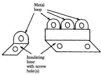
FIG. -9 Solder terminals are often used for point-to- point wiring. Metal
loop
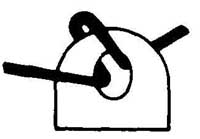
FIG. -10 The component leads are mechanically connected to the loop of the
solder terminal.
Loose, hanging wires can create their own problems, such as stray capacitances and inductances between them, which allows signals to get into the wrong portions of the circuit. The result is erratic or incorrect operation. Rats nest wiring is just begging for internal breaks within the connecting wires, and short circuits between them. Quite a bit of mechanical stress can be placed on some of the connecting wires. Momentary, intermittent shorts might not cause permanent damage in all cases, but they can result in some strange circuit performance that can be maddeningly frustrating to diagnose and service.
Perf boards
Simple to moderately complex circuits can be mounted on perf board (perforated board). A perf board is a nonconductive board with a regular pattern of holes or perforations drilled through it. Component leads are mounted directly through these holes. Alternately, special clips can be mounted in the holes and the component leads connected to the clips. The clips are commonly known as flea clips.
Perf board construction is essentially point-to-point wiring on a fixed base. The potential problems of rats-nest wiring can also show up in this construction method.
In any minimally complex circuit, one or more jumper wires can be required. A jumper wire is used to make a connection from one part of the board to another. If a jumper wire crosses any other wire or component, it must be insulated.
Take your time and experiment with component placement before you start soldering. Try to find an arrangement that will minimize the number of jumper wires and crossings used. Use straight line paths for jumpers whenever possible.
Another reason to experiment with the component placement before you start base with screw hole(s) soldering is to make sure all of the components will actually fit on the board. If you start soldering without checking this out first, you could find yourself facing some unpleasant surprises, like ending up with no place to mount that big filter capacitor.
Printed circuits
For moderate to complex circuits, or for circuits from which a number of duplicates will be built, a printed circuit (PC) board gives very good results. A nonconductive board is used as a base. Copper traces on one side (or, in very complex circuits, on both sides) of the board act as connecting wires between the components. Very steady, stable, and sturdy connections can be made, because the component leads are soldered directly to the supporting board itself.
Take great care in laying out a PC board to eliminate wire crossings as much as possible. Obviously, two copper traces cannot cross over each other (unless they are on opposite sides of the board). If a crossing is absolutely essential, an external wire jumper must be used.
Normally, components are mounted on the opposite side of the board from the copper traces. The component leads are fitted through holes drilled in the board and soldered directly to the copper pad on the opposite side of the board. Snip off the excess lead to reduce the chances of a short circuit and to create a more professional appearance. A typical PC board solder joint is shown in FIG. 11.
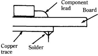
FIG. -11 A typical PC board solder joint. Copper trace; Solder.
Printed circuit board construction results in strong mechanical connections and very short leads. Lengthy leads actually get in the way. Short leads can help minimize interference and stray capacitance problems.
Stray capacitances between adjacent traces can adversely affect circuit performance. In some critical circuits, a guard band between traces can help reduce this potential problem. Especially in circuits using ICs (integrated circuits), the copper traces are often placed very close to one another. You must be extremely careful to avoid solder bridges. Use only small amounts of solder. If you use too much solder, it will flow and bridge across adjacent traces. Also watch out for short circuits from other causes. A small speck of loose solder, or a piece of a excess lead from a component could easily bridge across two (or more) adjacent traces, creating a short.
When soldering to a printed circuit (or PC) board, be very careful not to use too much heat or to apply heat for too long a time. Excessive heat can cause the copper foil trace to lift off the board. The unsupported trace is very fragile and will break.
Tiny, nearly invisible hairline cracks in the copper traces can also be a problem if you’re not careful. Generally, fairly wide traces that are widely spaced are the easiest to work with and the most reliable. However, this method isn’t always practical with all circuits—especially where ICs are used.
Blank boards for use as printed circuits are widely available. These are non-conductive boards with one side (sometimes both sides) completely covered with cop per foil. The desired pattern is put onto the board using a special resist ink. This process can be done either by photographic methods, or it can be drawn on directly with a special resist pen. The board is then soaked in a special acid solution, which eats away the exposed copper. The resist protects the portions of the copper foil it covers. The board is removed from the acid solution, and washed. The resist ink is removed, and the desired copper traces are left on the board.
Universal PC boards
There is a fairly recent form of printed circuit construction. Designing and etching a customized printed circuit board is a time-consuming and somewhat tricky job. Now you can buy various universal PC boards. These boards have a generalized pattern of copper traces, and can be used for many different circuits.
Wire wrapping
There is one type of permanent circuit construction that does not require soldering. This method is the wire-wrap method. It’s used primarily in circuits using large numbers of integrated circuits.
In a wire-wrapped circuit, a thin wire (typically 30 gauge) is wrapped tightly around a square post. The edges of the post bite into the wire, making a good electrical and mechanical connection without soldering. Components are fitted into special sockets that connect their leads to the square wrapping posts.
If you have just a few discrete components (resistors, capacitors, etc.), you can fit them into special sockets or solder them directly, and then wire wrap the connections to the ICs. If you use both soldering and wire wrapping, you have used what is called hybrid construction. In circuits involving many discrete components, the wire-wrapping method of construction tends to be rather impractical.
Wire-wrapped connections can be made (or unmade) quickly and easily, with out risking potential heat damage to delicate semiconductor components. Moreover, it usually is not difficult to make changes or modifications in the circuit.
Manual and electrical wire-wrapping tools are available. The tool is needed to wrap the wire tightly enough around the square post. Most wire-wrapping tools can also be used for unwrapping. Many of these tools can also cut the wire and strip off the insulation.
There are some disadvantages to this type of construction. Wire wrapping is awkward for use with discrete components. The thin wire-wrapping wire is very fragile and easily broken. It can carry only very low-power signals. In complex circuits, the wiring can be difficult to trace.
When many integrated circuits are involved (some advanced circuits require several dozen), wire wrapping can be a very convenient construction method.
<< >>