AMAZON multi-meters discounts AMAZON oscilloscope discounts
1. INTRODUCTION
Kaol first suggested the possibility that low-loss optical fibers could be competitive with coaxial cable and metal waveguides for telecommunications applications. It was not, however, until 1970 when Corning Glass Works announced an optical fiber with loss less than the benchmark level of 10 dB/km. After that, commercial applications began to be realised. The revolutionary concept which Corning incorporated and which eventually drove the rapid development of optical fiber communications was primarily a materials one--it was the realization that low doping levels and very small index changes could successfully guide light for tens of kilometers before reaching the detection limit. The ensuing demand for optical fibers in engineering and research applications spurred further applications. Today, we see a tremendous variety of commercial and laboratory applications of optical fiber technology.
2. HOW DOES AN OPTICAL FIBER WORK?
The optical fiber works on principles similar to other waveguides, with the important inclusion of a cylindrical axis of symmetry.
When light is travelling from one medium ( n 0 ) into a medium of different density ( n 1 ), a certain amount of incident light is reflected. This effect is more prominent where the light is travelling from a high-density medium into a lower-density medium. The exact amount of light that is reflected depends on the degree of change of refractive index and on the angle of incidence. If the angle of incidence is increased, the angle of refraction is increased at a greater rate. At a certain incident angle ( q C ), the refracted ray will have an angle of refraction that has reached 90° (that is, the refracted ray emerges parallel to the interface). This is referred to as the critical angle. For rays that have incident angles greater than the critical angle, the ray is internally reflected totally. In theory, total internal reflection is considered to reflect 100% of the light energy but in practice, it reflects about 99.9% of the incident ray.
FIG. 1 shows the generic optical fiber design, with a core of high refractive index surrounded by a low-index cladding. This index difference requires that light from inside the fiber which is incident at an angle greater than the critical angle be totally internally reflected at the interface.
A simple geometrical picture appears to allow a continuous range of internally reflected rays inside the structure; in fact, the light (being a wave) must satisfy a self-interference condition in order to be trapped in the waveguide. There are only a finite number of paths which satisfy this condition; these are analogous to the propagating electromagnetic modes of the structure. Fibers which support a large number of modes (these are fibers of large core and large numerical aperture) are called multimode fibers , whereas a fibers allowing only one mode of propagation are called single-mode fibers.
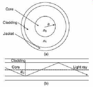
FIG. 1 (a) Generic optical fiber design (cross-section
view) (b) Path of a ray propagating at the geometric angle for total internal
reflection
3. SOURCES AND DETECTORS
This section will examine the operation of the optical sources and their associated detectors used with fiber optic systems.
3.1 Optical Sources
Effective optical sources for fiber optic systems need the following features:
To be able to effectively couple light into small fiber core, as small as 8.5 micrometers for single-mode fibers Easily modulated by electrical signals to convey data, with good linearity to prevent harmonics and inter-modulation distortion Provide high optical output power Have high reliability Small size and weight Low cost Light emitting junction diodes (LED) and laser diodes (LD) fulfill many of these requirements and we will now examine their properties in detail.
1. Light Emitting Diodes (LEDs)
LED is basically a specially designed p - n junction diode. LEDs can provide light output in the visible spectrum as well as in the 850 nm, 1350 nm and the 1500 nm windows.
Compared with the laser, the LED has a lower output power, slower switching speed and greater spectral width, hence there is more dispersion. These deficiencies make it inferior for use with high-speed data links and telecommunications. However, it is widely used for short- and medium-range systems using both glass and plastic fibers because it is simple, cheap, reliable and is less temperature dependent. It is also unaffected by incoming light energy from Fresnel reflections, etc. Although the lower power makes it safer to use, it can still be dangerous when the light is concentrated through a viewing instrument. Typical LED is shown in wires FIG. 2.
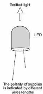
FIG. 2 Light Emitting Diode (LED)
Basic LED Operating Principles
When a positive voltage is applied to the p-region and a negative voltage applied to the n region, electrons and holes flow towards the junction of the two regions where they combine. When an electron combines with a hole, the atom returns to its neutral state and energy is released, having been converted into optical energy in the form of photons. In its simplest form, the radiated energy from the LED is caused by the recombination of the electrons and holes, which are injected into the junction by the forward bias voltage.
FIG. 3 illustrates this process.
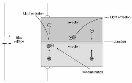
FIG. 3 Basic LED Operation
The size of the band gap determines the energy of the emitted photon. Different semiconductor materials have different band-gap energies and the gap energy ( W ) in electron-volts (eV) can be related to the wavelength ( l ) by the equation:
The usual LEDs applied in fiber optic systems use gallium aluminum arsenide (GaAlAs) for 800 to 900 nm wavelengths and gallium arsenide (GaAs) for 930 nm. LEDs for use with plastic fibers need to operate at about 660 nm and are produced with gallium arsenide phosphide (GaAsP) compounds. Various indium gallium arsenide phosphide (InGaAsP) compounds are used for longer wavelengths of 1300 and 1550 nm.
2. Lasers
Another form of LED is the laser diode. The most common form of laser diode is called an Injection Laser Diode (ILD) or just Injection Diode (ID). The word injection is not of interest-it merely refers to part of the process occurring inside the semiconductor material. A laser provides a light of fixed wavelength which can be in the visible region around 635 nm or in any one of the three infrared windows. The light has a very narrow bandwidth, typically only a few nanometers wide. This ensures that chromatic dispersion is kept to a low value and this, together with fast switching, allows high data-transmission rates. As the laser device itself is barely visible to the unaided eye, it must be contained in some form of package. Two typical examples are shown in FIG. 4 .
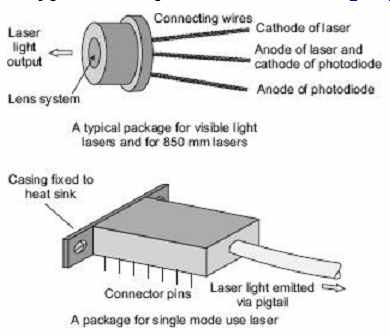
FIG. 4 Typical laser diode
Basic Principles of Laser Operation
LASER stands for Light Amplification by the Stimulated Emission of Radiation. LEDs and lasers use very similar principles of operation. In the earlier section of LED, it has been discussed that light is emitted from an LED when an electron drops from a high energy level to a lower one. When this occurs without outside influence, it is known as spontaneous emission. This occurs in some radioactive material. With the LED discussed in the previous section, a forward-bias voltage was used to stimulate the emission. An electron sitting at the upper energy level can also be stimulated to drop to the lower level by a photon with the right amount of energy. In this way, the external photon can stimulate the emission of a second photon at the same wavelength. Laser action takes place through optical resonance. The laser structure is very similar to an edge LED, having a thin, narrow active region with the addition of reflective-end facets and reflective sides as shown in FIG. 5. In this resonator, the light is confined and reflected backward and forward through the excited medium. The laser is biased to begin the emission of photons. The photons reflect backward and forward and stimulate further emission of photons from electrons waiting to recombine. The light travelling back and forth along the axis of the resonator continues this action and builds up in strength until it is strong enough to break through the reflective end and thus, a laser beam is formed.
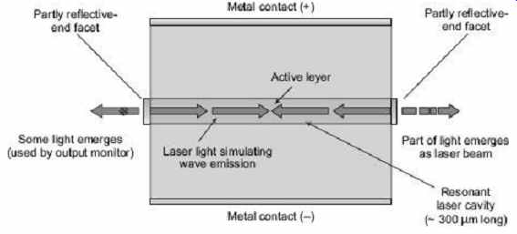
FIG. 5 LASER source
3.2 Optical Detectors
The function of the optical detector is to efficiently convert the small amount of light energy received from the fiber, as photons, into electrical signals. The detector needs to be a low inherent noise device, incorporating appropriate amplification to generate useful output signals from low level inputs. Two main types of devices are used for practical detectors: PIN diodes and avalanche photodiodes.
1. PIN Diodes
The PIN diode is very widely used as a detector for converting light energy received from the optical fiber into an electronic signal. The PIN diodes look like LEDs. The difference is in its construction. The name 'PIN' stands as 'P' for p -type semiconductor, 'I ' for intrinsic semiconductor and ' N ' stands for n -type semiconductor. In this case, the intrinsic layer is in the middle position and one side covers the p -type semiconductor whereas the other side covers the n -type semiconductor. Hence, it is called P-I-N or PIN diode.
The Theory of its Operation
The PIN photodiode has a wide intrinsic semiconductor layer separating the p- and n -regions, as shown in FIG. 6 . The diode is reverse biased (4.5-18 volts) and this helps draw the current carriers away from the intrinsic region. The width of the intrinsic layer ensures that there is a high probability of incoming photons being absorbed in it rather than in the p- or n-regions. The intrinsic layer has a high resistance because it has no free charges. This results in most of the diode voltage appearing across it, and the resultant electrical field raises the response speed and reduces noise. When light of suitable energy strikes the intrinsic layer, it creates electron-hole pairs by raising an electron from the valence band to the conduction band and leaving a hole behind in the process. The bias voltage causes these current carriers (electrons in the conduction band) to quickly drift away from the junction region, producing a current proportional to the incident light, as shown in FIG. 6 .
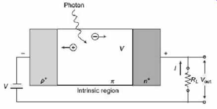
FIG. 6 Theory of operation, PIN photodiode
2. Avalanche Diode/Avalanche PhotoDiode (APD)
Avalanche photodiodes are used where very weak light signals have to be amplified, and converted into a strong electrical signal. These diodes work on higher operating voltages, i.e. reverse-bias voltage is very high, now whenever a small amount of light energy falls on the intrinsic region, avalanche breakdown occurs and hence large reverse bias current flows through the circuit. The main advantages of APD are good output at low light levels and a wide dynamic range-it can handle high and low light levels. The disadvantages of APDs are higher noise levels, higher cost, requires higher operating voltages and its decrees of gain with an increasing temperature.
Operating Principles
Avalanche photodiodes use semiconductor junction detectors with internal gain through avalanche current multiplication. A very high reverse bias voltage (50-300 volts) is applied to a p - n junction. A photon is absorbed in the depletion region, creating a free electron and a free hole. These charges accelerate in the strong electric field. When they collide with neutral atoms in the crystal lattice, their kinetic energy is sufficient to raise electrons across the band gap and create additional electron-hole pairs. These secondary charges also accelerate creating more electron-hole pairs. In this way, the current produced by one photon is multiplied.
The p + and n + layers are highly doped regions with very small voltage drops as shown in FIG. 7. The depletion region is lightly doped, almost intrinsic. Most of the photons are absorbed in this area, forming electron-hole pairs. The electrons move to the p - region that has been depleted of free charge by the large reverse voltage. The depletion region at the p + n + junction effectively reaches right through the p-layer. The strong electric fields across the p -layer cause avalanche multiplication of the electrons. The holes produced drift across the p layer to the p + electrode but do not cause further multiplication. Because this structure limits the charge carrier multiplication to electrons only, it has better noise performance.
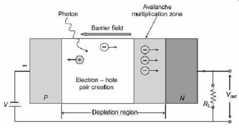
FIG. 7 Theory of operation, avalanche photodiode
4. FIBER OPTIC POWER MEASUREMENT
4.1 Optical Power
The fundamental unit of measure used in fiber optics is light power. As with electric power, optic power is measured in watts.
For light, the total energy Q is given by
Q = NQ p
where, Q p is the energy of a single photon and N is the number of photons
Therefore,…
Power Meter
Power in a fiber optic system is like voltage in an electrical circuit-it's what makes things happen. It is important to have enough power, but not too much. Too little power and the receiver may not be able to distinguish the signal from noise; too much power overloads the receiver and causes errors too.
Measuring power requires only a power meter (most come with a screw-on adapter that matches the connector being tested) and a little help from the network electronics to turn on the transmitter. During the measurement of power, the meter must be set to the proper range (usually dBm, sometimes microwatts, but never "dB" a relative power range used only for testing loss) and the proper wavelengths matching the source being used. FIG. 8 shows the technique used in the measurement of optical power.
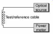
FIG. 8 Measurement of optical power
To measure power, attach the meter to the cable that has the output you want to measure. That can be at the receiver to measure receiver power, or to a reference test cable (tested and known to be good) that is attached to the transmitter, acting as the "source", to measure transmitter power. A typical power meter is shown in FIG. 9 . Turn on the transmitter/source and note the power the meter measures. Compare it to the specified power for the system and make sure it has enough power but not too much.
For the power meter as shown in FIG. 9 , the wavelength is adjustable over the three windows and some offer a facility to step up and down by small increments. This allows the fiber characteristics to be quoted at any required wavelength. It is a 'nice to have' rather than an essential feature. The power levels can be indicated in mW or in decibels as dBm, relative to one milliwatt or as dBr, relative to a previously noted value.
They are available with internal memories to store the day's work and a thermal printer for hard copies.
If the light source and power meter are to be used to Measured power check an installation or repair on a commercial basis, the customer will need assurance that reading of the power meter is correct. The proof of this is provided by a calibration certificate for each instrument which must be renewed at intervals, usually annually. The calibration must be carried out by an authorized company whose instruments themselves are calibrated against the appropriate national standards. In this way, we can trace the accuracy back to its source.
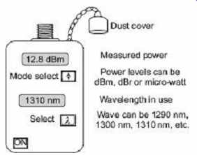
FIG. 9 Typical power meter
4.2 Measurement of Loss
It is basically the difference between the power coupled into the cable at the transmitter end and what comes out at the receiver end. Testing for loss requires measuring the optical power lost in a cable (including connectors, splices, etc.) with a fiber optic source and power meter by connecting the cable being tested to a known good reference cable.
For loss measurement, a power meter along with a test source is required. The test source should match the type of source (LED or laser) and wavelength (850, 1300, 1550 nm).
There are two methods that are used to measure loss, which we call "single-ended loss" and "double-ended loss". Single-ended loss uses only the launch cable, while double-ended loss uses a receive cable attached to the meter.
Single-ended loss is measured by mating the cable under test to the reference launch cable and measuring the power output at the far end with the meter. By doing this, total loss is being measured that is loss of the connector mated to the launch cable and the loss of any fiber, splices or other connectors in the cable under test. This method is described in FIG. 10 . Reverse the cable to test the connector on the other end.
For the measurement of double-ended loss attach the cable to test between two reference cables, one attached to the source and one to the meter. In this way, two connectors' losses are being measured one on each end, plus the loss of all the cable or cables in between. This method is shown in FIG. 11 .
We also need one or two reference cables, depending on the test. The accuracy of the measurement will depend on the quality of your reference cables. Reference cables always need to be tested by the single-ended method discussed earlier, to ensure they are good before starting the test of other cables.
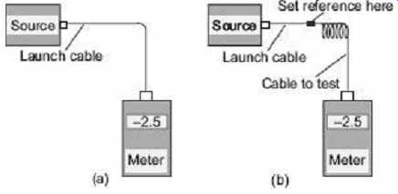
FIG. 10 Single ended loss measurement
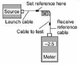
FIG. 11 Double ended loss measurement
Example 1 Calculate the approximate loss at wavelengths of 1300 nm and 1550 nm for a optical system having 2 connectors, 2 splices and a single-mode optical fiber with a length of 10 km.
Solution
For each connector, loss is 0.5 dB.
For each splice, loss is 0.2 dB For the single-mode fiber, the loss is about 0.5 dB per km for 1300 nm sources, and 0.4 dB per km for 1550 nm.
So approximate loss is (0.5 × 2 + 0.2 × 2 + 10 × 0.5 ) dB for 1300 nm wavelength = 6.4 dB and (0.5 × 2 + 0.2 × 2 +10 × 0.4) dB for 1550 nm wavelength = 5.4 dB
4.3 Optical Time Domain Reflectometer (OTDR)
The most commonly used and best recognized method of analyzing the state of a fiber optic link is to test it with an Optical Time domain Reflectometer (OTDR). The OTDR uses backscattered light of the fiber to imply loss. The OTDR works like RADAR, sending a high power laser light pulse down the fiber and looking for return signals from backscattered light in the fiber itself or reflected light from the connector or splice interfaces. By measuring the time it takes for the reflected light to return to the source and knowing the refractive index of the fiber, it is possible to calculate the distance to the reflection point.
When this instrument is connected to one end of any fiber optic system up to 250 km in length, within a few seconds, it is able to measure the overall loss, or the loss of any part of a system, the overall length of the fiber and the distance between any points of interest.
1. Operating Principle
As light travels along the fiber, a small proportion of it is lost by Rayleigh scattering. As the light is scattered in all directions, some of it just happens to return back along the fiber towards the light source. This returned light is called backscatter . The backscatter power is a fixed proportion of the incoming power and as the losses take their toll on the incoming power, the returned power also diminishes as shown in FIG. 12.
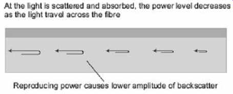
FIG. 12 Loss due to Rayleigh scattering
The OTDR can continuously measure the returned power level and hence deduce the losses encountered on the fiber. Any additional losses such as connectors and fusion splices have the effect of suddenly reducing the transmitted power on the fiber and hence causing a corresponding change in backscatter power. The position and the degree of the losses can be ascertained.
Example 2 An optical fiber has a core of refractive index of 1.5. When the fiber is being tested with an OTDR system, it shows a sharp fault peak after with delay of 1.4 μs. Find the possible distance of fault.
Solution
Travelling speed of light through the core is ...
This means that it will take 5 ns to travel the distance of 1 m.
If the OTDR measures a time delay of 1.4 ms then the distance travelled by the light is The 280 meters is the total distance travelled by the light and is the 'onwards and return' distance. The fault location is therefore only 140 m.
2. Inside the OTDR
In general, an OTDR system has the following inside components:
(a) Timer
The timer produces a voltage pulse which is used to start the timing process in the display at the same moment as the laser is activated.
(b) Pulsed Laser
The laser is switched on for a brief moment, the 'on' time being between 1 ns and 10 ms. The wavelength of the laser can be switched to suit the system to be investigated.
(c) Directive Coupler
The directive coupler allows the laser light to pass straight through into the fiber under test. The backscatter from the whole length of the fiber approaches the directive coupler from the opposite direction. In this case, the mirror surface reflects the light into the avalanche photodiode (an APD). The light has now been converted into an electrical signal.
(d) Amplifying and Averaging
The electrical signal from the APD is very weak and requires amplification before it can be displayed. The averaging feature is quite interesting and we will look at it separately towards the end of this section.
(e) Display
The amplified signals are passed on to the display. The display is either a Cathode Ray Tube (CRT) like an oscilloscope or a computer monitor, or a liquid crystal as in calculators and laptop computers. They display the returned signals on a simple XY plot with the range across the bottom and the power level in decibels up the side.
(f) Data Handling
An internal memory or a floppy disk drive can store the data for later analysis. The output is also available via an RS232 link for downloading to a computer. In addition, many OTDRs have an onboard printer to provide hard copies of the information on the screen. This provides useful 'before and after' images for fault repair as well as a record of the initial installation. Inside components of a typical OTDR system are shown in FIG. 13 .
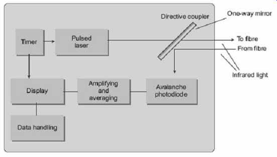
FIG. 13 Functional block diagram of an OTDR
system
3. Measurement Using OTDR
Impurities in the glass will cause a continuous low level reflection as the light travels through the glass fiber. This is referred to as backscatter. The correct technical term of this is Rayleigh scattering . The strength of the backscatter signal received at the source gradually drops, as the pulse moves away from the source. This is seen on an OTDR as a near linear drop in the received reflected signal and the slope of this linear drop is the attenuation of the fiber (dB per km). FIG. 14 illustrates a typical reflection curve for an OTDR and notes the backscatter. Generally, an OTDR will not provide accurate readings of irregularities and losses in the fiber for the first 15 m of the cable. This is because the pulse length and its rise time from the OTDR are comparatively large when compared to the time it takes for the pulse to travel the short distance to the point of reflection within this 15 m and back. To overcome this problem, a reel of cable is inserted between the OTDR and the link to be tested. When reading the OTDR screen, the first length of cable is ignored and is referred to as the dead band . With reference to the OTDR plot in FIG. 14 , the Y -axis of the plot shows the relative amplitude of the light signal that is reflected back to the source and the X-axis represents time. The time base is directly translated and displayed as distance by the OTDR.
The sudden peaks that appear along the slope are the points where reflections have occurred and the light that has reflected back to the source is stronger than the backscatter.
There are five main reflection points illustrated in FIG. 14. In their order of decreasing magnitude, they are
1. Reflection from the unterminated end of the fiber
2. Reflection from a connector
3. Reflection from a splice
4. Reflection from a hairline crack in the fiber
5. Backscatter After each of the reflections, the slope of the attenuation curve drops suddenly. This drop represents the loss introduced by the connector, splice or imperfection in the fiber.
Point (6) noted in FIG. 14 illustrates a splice where the cores of fibers are well matched for light travelling in the direction away from the source. This splice has no reflection but just a loss introduced by the splice. The type of drop at the point (6) in the attenuation curve could also be caused by a sharp bend in the fiber where light escapes out of the fiber at the bend and is not reflected back. Some types of faults in the fiber will also cause similar results.
Point (7) noted in FIG. 14 shows the noise floor of the instrument. This is the lowest sensitivity of a received signal that the device can accept. Measurements made close to this level are not very accurate. OTDR testing can provide very accurate fault analysis over almost any length of fiber. It is important that the deadband roll of cable is always inserted between the OTDR and the link before making the measurement. On the better quality instruments, a resolution of 1 m for fault location and .01 dB for in-line losses can be obtained. Some instruments will operate with a range of up to 400 km.
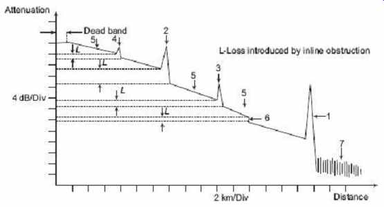
FIG. 14 Trace from an OTDR
QUIZ
Objective-type Questions
1. Light passes through the fiber due to phenomena of (a) total internal reflection (b) reflection from the interface of two medium (c) transmission to the second medium (d) both transmission and reflection at the interface of two medium
2. LEDs operating in the wavelength of 800-900 nm are mainly made of (a) GaAs (b) GaAlAs (c) GaAsP (d) InGaAsP
3. The width of active region of LASER diode is comparatively (a) wider that LEDs (b) almost equal to LEDs (c) much wider that LEDs (d) narrower than LEDs
4. PIN photodiodes are kept in (a) forward bias (b) reverse bias (c) connected circuit and no bias voltages are given (d) initially forward biased and then reverse biased
5. Avalanche photodiodes have output voltage comparatively (a) lower that PIN photodiode (b) higher than PIN photodiode (c) higher than normal photodiode (d) higher than normal and PIN photodiode
6. In OTDR response, the peaks of the reflected waveform do not occur due to: (a) reflection from the unterminated end of the fiber; (b) reflection from a connector; (c) backscatter; (d) reflection from the interface of core and cladding

Short-answer Questions
1. How do light waves travel through an optical fiber? Explain with a proper diagram.
2. State the working principle of a p - n junction photodiode.
3. How are LASER diodes different from LEDs? How do LASER diodes generate LASER light?
4. How do PIN diodes work? What are the benefits of avalanche diodes and how do they work?
5. How is the optical power in a fiber optic network measured? Explain in brief.
6. State the procedures adopted during the measurement of fiber loss.
7. How does the OTDR work? Explain in brief with a diagram.
8. Draw the functional block diagram of a typical OTDR system and explain in brief about each element.
9. How are different reflective components measured using an OTDR system?
10. Calculate the approximate loss at wavelengths of 800 nm and 900 nm for an optical system having 1 connector, 4 splices and a single-mode optical fiber with a length of 10 km.