AMAZON multi-meters discounts AMAZON oscilloscope discounts
1. SYNTHESIS AND ARCHITECTURE OF A SEMICONDUCTOR CHIP FOR ESD PROTECTION
In on-chip electrostatic discharge (ESD) circuit design, the design architecture and synthesis is critical in achieving ESD robustness. This Section will briefly address the fundamental of the physical elements in ESD design. In ESD design, there are fundamental elements needed in the chip design synthesis to establish an alternative current loop to prevent the ESD current from causing chip or system damage. In ESD design, the fundamental elements in the design synthesis are the following:
_ ESD input protection networks
_ ESD power clamps networks
_ ESD rail-to-rail networks
_ Guard rings
In ESD design, the ESD robustness of the system will be a function of the following:
_ Placement
_ Physical size
_ Triggering conditions
_ Inherent robustness of the ESD circuitry
_ Inherent robustness of the circuits that require protection FIG. 1 shows an example of an ESD input circuit, power rails, and an ESD power clamp network.
The high-level schematic highlights the electrical connectivity between the pad and both power rails. Additionally, the ESD power clamp also establishes electrical connections to both power rails.
2. ELECTRICAL AND SPATIAL CONNECTIVITY
In an ESD design, the inter-relation of the elements in the system is key in achieving ESD robustness. The inter-relationship and interaction of the physical elements in the system can be dependent on both electrical connectivity and spatial connectivity. The electrical connectivity between a first electrical node and a second electrical node in the system will influence the ESD robustness of a design, chip, or system. The spatial connectivity between a first spatial point and a second spatial point can also influence the ESD robustness of a semiconductor chip. Depending on the ESD mechanism, the issue of the spatial relationship is not always critical.
2.1 Electrical Connectivity
Electrical connectivity is an important concept in ESD design. It is critical to establish a design architecture that allows electrical connectivity between external pins and power rails, and power rails to power rails. To establish good ESD robustness, current must be able to flow from external pins connections to power rails. Hence, a current path must exists which allows between all physical external node (e.g., input/output circuits, peripheral circuits). A power boundary condition can be stated that states that the flow of current must be able to flow from any node which connects to outside the system to any second node (e.g., a second input pin, or power rail) within the physical system. A second condition is that current must be able to flow from one power rail to a second power rail. In order to achieve this, electrical connectivity must exist between a first and second power rail, where the first and second rail do not have to be at the same bias condition.
In order to provide ESD protection, a Kirchhoff current loop can be established between the first node and the grounded reference power supply. The input source serves as part of the Kirchhoff current loop from the ground, through the source element, the electrical switch, and the input node of the device under test (DUT). The Kirchhoff current loop continues to the grounded reference and back to the ground plane. In the case of power supply to power supply, the Kirchhoff current loop does not contain the input pin but from a first power supply to second power supply.
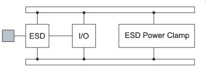
FIG. 1 High-level electrical schematic highlighting the electrical connectivity
between the pad, ESD network, power rails, and the ESD power clamp
2.2 Thermal Connectivity
Thermal connectivity, analogous to the electrical connectivity, also plays a role in ESD protection in a system. A thermal circuit contains thermal components and thermal nodal points. The thermal network can be associated with a point in the circuit or spatial location.
There are temperature values associated with the thermal nodal points. Through the substrate region, components interact through thermal coupling. In the thermal equivalent circuit, the thermal coupling can be represented as thermal transfer resistance terms and thermal feedback phenomenon. Thermal interaction between adjacent structures can play a role in current and voltage distribution.
2.3 Spatial Connectivity
Spatial connectivity also plays a role in ESD protection. The primary reason for issues of a spatial nature is ESD phenomena which is interactive through the silicon substrate.
Through the substrate, both electrical and thermal physical phenomena exist. From an electrical perspective, there is inductive and capacitive coupling, as well as minority carrier injection phenomena. There are also initial conditions where uniform charge exists in the substrate prior to electrical discharge. For example, in the charge device model (CDM) test, the substrate is charged across the entire substrate region. The spatial relationship between input pads, peripheral circuits (e.g., off-chip drivers (OCD), receivers, transmitters), wire interconnects, ESD input circuit networks, ESD power clamps, and busses can play a critical role in the ESD response of a network (FIG. 1). When addressing the spatial dependence, the physical time constants of the system are critical in the understanding of the semiconductor circuit response. These can include the charge relaxation time, the carrier diffusion time, and the circuit time constant response of the network involved in the CDM event. FIG. 2 denotes the interaction of the electrical, thermal, and spatial connectivity.
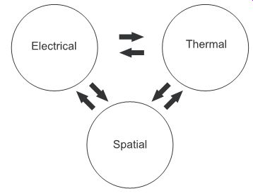
FIG. 2 Electrical, thermal, and spatial connectivity
3. ESD, LATCHUP, AND NOISE
ESD protection, latchup, and noise are all influenced by the electrical, thermal, and spatial connectivity in a chip or system. Providing good electrical connectivity between segments of a chip or a system can provide improved ESD protection, but at the same time introduce noise concerns. Consequently, providing good noise isolation can lead to poor ESD protection; this does not have to be true. Choosing the right design choices in the synthesis of the design segments, circuit set, and the ESD protection type can allow for achieving both good noise isolation as well as good ESD robustness.
ESD, latchup, and noise are also dependent on the process technology and the substrate region. The choice of the n-well, p-well, triple-well, and substrate doping concentrations have a strong influence on all three issues. Typically, higher well doses can lead to lower parasitic bipolar current gain in parasitic transistor elements. This also reduces the noise injection into the substrate region. When using diode-based ESD solutions, it was shown that higher well doses lead to improved ESD diode performance. On the other hand, using MOSFET-based ESD protection leads to a lowering of the MOSFET second breakdown with higher well doses. In the case of the substrate doping concentration, lower substrate doping concentration improves noise isolation. At the same time, the minority carrier lifetime in the substrate improves, leading to a greater concern of latchup initiation from minority carriers.
3.1 Noise
There are many design practices to reduce noise in a chip. Some noise reduction techniques have no influence on ESD robustness or latchup. Some of these design practices may also be good solutions for ESD protection and latchup minimization. Many noise prevention and reduction techniques have been proposed by Verghese, Schmerbeck and Allstot. Noise prevention can be achieved by reduced noise generation through avoiding switching large transient supply current, reduced I/O driver generated noise, and lower switching function bus impedance.
Switching large transient supply currents is a function of whether the circuitry uses balanced current steering logic or voltage switching internal logic families. Noise reduction can also be achieved by power management. This is achievable by shutting down switching functions, logic circuits, or OCD networks. The I/O driver noise generation can be reduced by temporal and spatial placement solutions of the networks. For example, temporal improvements in the noise is achieved by avoiding simultaneous switching of I/O circuits, use of slower OCD circuits, use of voltage rise time-controlled networks, and use of balanced current steering OCD networks. Placement of the drivers close to the power rail returns reduces the network inductance. Use of lower switching function bus impedance is achievable using multi-level and grid-like design, adding distributed on-chip decoupling capacitors, and providing a maximum number of chip power pad/pin ratio. Noise reduction techniques can be achieved by isolating sensitive circuits and providing noise-tolerant circuits. Isolation of sensitive circuits can be achieved by maximizing the impedance between the noise source and the sensitive circuits. This can be achieved by spatial separation and semiconductor process choices of the semiconductor substrate. Noise isolation of the sensitive circuit can also be achieved using guard rings, isolation structures, substrate contact, and shielding films or regions [3]. Many of these solutions for noise reduction are also good solutions for ESD protection and latchup in semiconductor components.
3.2 Latchup
Latchup occurs in semiconductor technology as a result of the presence of a parasitic pnp and npn bipolar transistor forming a pnpn (e.g., silicon controlled rectifier). Latchup robustness is a strong function of semiconductor technology in CMOS and BiCMOS technology. The electrical, thermal, and spatial connectivity can influence the latchup robustness of a semiconductor chip. Latchup can be both a local as well as global phenomena in a semiconductor chip. The electrical connectivity of pads, circuits, and circuit functional blocks can influence the latchup robustness of a semiconductor chip.
The placement of pads, circuits, circuit function, power rails, and the architecture of the semiconductor chip or system can also play a key role in the latchup sensitivity. As with noise, the relative placement of injection sources, and latchup-sensitive circuits is key to latchup robustness. Analogous to the noise issue, semiconductor process choices and semiconductor layout design influences latchup sensitivity. Substrate contacts, isolation structures, and the relative placement of circuits influence the spatial and electrical coupling which occurs in the semiconductor chip. Hence, the spatial and electrical solutions can influence noise, latchup, and ESD protection (FIG. 3). Latchup design practices, as is true in ESD design practice, can involve the following concepts:
_ Addressing high current and high voltage sources.
_ Involvement of parasitic elements.
_ Utilization of guard rings.
_ Decoupling from power supply and ground connections.
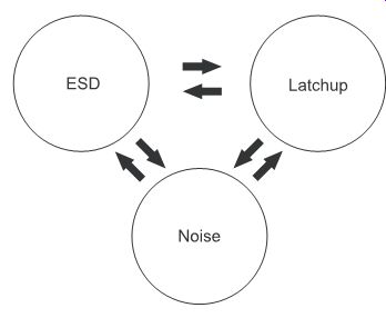
FIG. 3 ESD, latchup, and noise
4. INTERFACE CIRCUITS AND ESD ELEMENTS
Circuits and structures that interface with the external environment are vulnerable to electrical overstress (EOS), ESD, and latchup events. To prevent the failure of semiconductor components, circuits, or chips from ESD events, the circuits must be suitable to absorb the ESD event without damage to the circuit function. In the majority of cases, additional elements are added to the circuit whose function is to provide additional protection to the circuit element. The network choices are dependent on the circuit function, performance requirements, and allowed chip area. The choice of the type of network is also a function of the input stimulus or the ESD event.
ESD networks are placed on the input pads of the circuits which interface with the external environment. Typically, ESD protection networks are placed in the semiconductor substrate and are composed of the same material as the semiconductor chip. In this fashion, the ESD protection networks are constructed out of the same materials and devices as the semiconductor process to which it is to provide the ESD protection. The fact that the ESD protection elements comprise the same technology it is to provide the ESD protection produces a challenge in that each technology will have a different operation and ESD performance.
ESD networks are placed on input pins (e.g., or connected to the input pads) for all circuits. According to Rent's rule, as the number of logic gates increases, the number of input/output (I/O) circuits also increases as...
NI=O = ANC () B
where NI/O is the number of I/O pads, NC is the number of circuits, and the parameter A and B are constants. Given that the all I/O pads require an ESD protection network, then NI/O = NESD; hence...
NESD = A(NC) B
...where NESD is the number of I/O ESD networks needed for a semiconductor chip.
Given a chip design contains an I/O network equal to area defined as AI/O (e.g., area of a given I/O network) then the total area (AI/O)T estimated for the I/O networks can be assumed to be approximately ...
(AI=O)T = AI=ONI=O =(AI=O)A(NC) B
In typical implementations, the area of the ESD networks is a percentage of the total area dedicated to the I/O networks. The depending on the circuit, the application, and the ESD objectives, the percentage of the area can vary from 10 to 50% of the I/O network area.
Defining a variable which represents the ratio of ESD area to the I/O cell area (e.g., kESD, where kESD varies from 0 to 1), we can estimate the total chip area dedicated to ESD protection of the input pads as...
AESD ()T= kESDAI=ONI=O = kESD(AI=O)A (NC) B
ESD networks on input (input or output) pads are designed to provide protection against human body model (HBM), machine model (MM), charged device model (CDM), and fast pulse phenomena that occurs on the physical pads. ESD networks can also serve as providing circuit protection from over- and under-voltage phenomena. The ESD networks can provide clamping function which assists in both over-voltage protection as well as chip functional performance.
ESD networks used for input pads in a peripheral I/O environment are placed near the physical pads for the given circuit function. In some chip architectures, OCD networks are grouped in a semiconductor design. In an ''array I/O'' chip architecture, ESD networks are placed near the I/O circuit itself and are not local to the input pad. Hence, the ESD network is placed local to either the pad itself or the circuit itself, depending on whether the placement is on the chip boundary, or grouped in ''I/O banks,'' or in an array. The architecture of the chip and floor plan will determine the placement. The placement of the pad, the relative distance between the pad and ESD network, and the relative distance between the ESD network and the I/O device can influence the ESD robustness of the system. The electrical connectivity and spatial connectivity play a role; this is most critical with CDM failure protection.
ESD networks can be constructed to provide ESD protection from multiple types of events, where different circuit elements play a different role.
To provide ESD protection from HBM or MM events, a network is required to allow current flow of a positive or negative polarity which is applied to the input pad. HBM event waveforms are a damped double-exponential waveform of a single polarity. These events can be of a positive or negative polarity. As a result, an element is required for both types of events. For example, a double-diode network (FIG. 4) can provide against both positive and negative ESD events.
To provide ESD protection against an MM event, the network must provide protection against an oscillatory waveform which oscillates from positive to negative polarity within a given pulse event at the input pad node. In the HBM event, only one polarity occurs at a given event. In these processes, the location or placement of the ESD network relative to the input pad is not crucial.
To provide ESD protection against CDM events, the spatial placement of the protection scheme relative to the vulnerable circuit element is very important. In the case of the CDM event, the substrate region is charged prior to the discharge process. As a result, the source of charge or current is not initially at the input pad, but contained within the semiconductor chip or package. In this case, the relative placement of the charge source and all physical elements in the network relative to the grounded pad is critical to the protection strategy. In a CDM event, the substrate doping concentration and the substrate charge relaxation time play a role in how the charge transfers to the various elements.
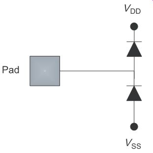
FIG. 4 Circuit with double-diode ESD network
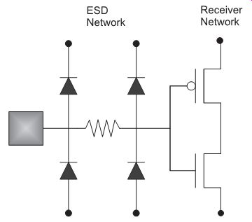
FIG. 5 Example of a ESD network
A circuit type which is sensitive to the CDM event are MOSFET receivers. A typical case is a MOSFET inverter input connected to an input pad. The MOSFET receiver input is connected to the gate of the p-channel MOSFET pull-up device and the gate of the n-channel MOSFET pull-down device. In a p-substrate wafer, the n-channel MOSFET gate is vulnerable to ESD damage during a CDM event. As the substrate is charged positively, and the input pad is grounded, the potential on the MOSFET inverter gates are at a ground potential. Charge from the substrate flows through the MOSFET gate dielectric structure. In this case, the MOSFET dielectric failure will occur. To avoid this issue, a p-n diode is needed local to the MOSFET gate whose impedance is lower. At the time constant of the discharge process, if the impedance through the diode structure is lower than the impedance of the MOSFET gate structure then the p-n junction will ''current rob'' the CDM current, avoiding destruction of the MOSFET gate structure. In this case, the spatial location of the CDM p-n diode and its net impedance will play a role in the effectiveness of protecting the MOSFET gate structure. By placement of an ESD protection n-diffusion device in the p-substrate spatially local to the gate, the holes flow from the substrate across the p-n metallurgical junction formed between the substrate and the n-region contained in the substrate (FIG. 5).
5. ESD POWER CLAMP NETWORKS
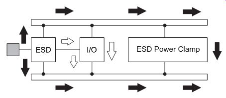
FIG. 6 Illustration of the circuit Kirchhoff current loop and the ESD
Kirchhoff current loop.
In the architecture of systems and chip design, a current loop exists between the pad and the input circuit to a reference point. The ESD current loop is in parallel with the circuit current loop. The objective of the ESD current loop is to allow the current to flow through this bypass current loop avoiding failure of the sensitive circuits. In the ESD Kirchhoff current loop, ESD input element allows the current to flow from the input pad to the power rails of the system. In order for the current to flow to the grounded reference rail, the ESD current must flow through the power grid, and from one power rail to another to complete the ESD Kirchhoff current loop. The effectiveness of the ESD system is a function of the sum of the effectiveness impedance of the ESD Kirchhoff current loop (FIG. 6).
In very large systems, significant capacitance can exist between the power rails. The impedance between the power rails is inversely proportional to the product of the frequency of the ESD event and the capacitance, Ceff, between the power rails.
Z ! ()= 1 j w ESD Ceff
In large systems, or large semiconductor chips, the impedance between the VDD power rail and VSS power rail can be small. With technology evolution and scaling, the sensitivity of the circuits has increased, requiring a lower impedance through the ESD Kirchhoff current loop.
Additionally, to achieve higher circuit performance the ESD input node circuit capacitance must be reduced. As the signal ESD structures are reduced in size, the impedance of these elements will increase. This increases the requirement for a lower power rail impedance in order to maintain a constant impedance through the ESD Kirchhoff current loop.
With technology scaling and integration, noise is also a concern. To minimize noise, regions of the systems are separated to reduce noise coupling between circuits. This is achieved by creation of many separated power supply and ground rails. As the power rails are separated into smaller domains, the ESD Kirchhoff current loop is limited to a smaller chip region, increasing the effective chip capacitance and the impedance.
To improve the effectiveness of the ESD Kirchhoff current loop, ''ESD power clamps'' are placed between the power rails (e.g., VDD and VSS) to lower the effective impedance. In the case where no ESD power clamps are placed in the network, the system will find a current path which is the lowest impedance path. By placement of the ESD power clamp in the system, the current flow can be directed through specified current paths.
ESD events can also occur on the power rails. In this case, the ESD power clamp establishes a ESD Kirchhoff current loop to the grounded reference point. The ESD power clamp also serves the role of establishing a low-impedance path to establish the direction of the current flow. As a result, the ESD power clamps serve a dual role of providing improved input pad protection and power rail-to-power rail connection.
ESD power clamps then provide electrical connectivity to nodal points in a system to allow the current flow from node to node. Whereas the functional objective of the system is to provide both spatial and electrical separation, the ESD power clamp plays the role of reestablishing electrical connectivity during ESD events.
The ESD power clamp networks can consist of passive or active elements. Active elements can consist of semiconductor components in the technology. ESD power clamps can consist of active elements such as n-channel or p-channel MOSFETs, and bipolar transistors. ESD power clamp elements can also contain passive elements such as resistors and capacitor elements.
The ESD power clamps can be initiated by frequency or voltage triggering. As a result, different classes of ESD power clamps exist, with tradeoff in each implementation (FIG. 7). In all cases, the ESD power clamp functional objective is not to be activated during a chip power-up or power-down, not to interfere with system functionality, and to activate during ESD events. Frequency-triggered ESD power clamps remain ''off'' during dc phenomenon but respond to the ''ac'' signal induced by the ESD pulse event (FIG. 8).
Voltage-triggered ESD power clamps remain ''off'' during normal voltage conditions and chip operation, but turn ''on'' when a voltage condition is exceeded. This can be an over voltage condition, overshoot or undershoot phenomenon, or any high current event.
5.1 Placement of ESD Power Clamps
In the floor plan of the system or semiconductor chip, the placement of the ESD power clamps can influence their effectiveness. In the system or semiconductor chip, the power rail distribution has both resistance, capacitance, and inductive characteristics that can influence the current distribution in the ESD Kirchhoff current loop. These impedance characteristics will provide a distributed nature to the current flow through the system. It is the impedance characteristics of the power rail system which will influence the floor plan and placement of the ESD power clamps.
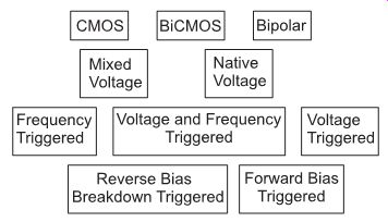
FIG. 7 Example of classes of ESD power clamps
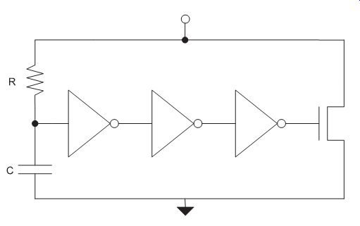
FIG. 8 A frequency-triggered ESD power clamp
The second aspect of importance of the floor plan is the location of the signal pins (e.g., as well as corresponding ESD signal pin network) relative to ESD power clamps. The signal pin, the distributed power grid, and ESD power clamp element are contained in the ESD Kirchhoff current loop. As the signal pin distance increases from the ESD power clamp element, the ESD current must flow through a farther distance through the power grid. As the distance increases, there will be a limitation of the total impedance in the ESD Kirchhoff current loop which will limit the effectiveness of the ESD system. In this case, the placement is an electrical connectivity and electrical impedance defining the spatial positioning of the ESD power clamps relative to the signal pins.
In the floor plan of a chip design, there are other tradeoffs and issues that influence the placement of the ESD power clamps. ESD power clamps can be the sources of minority carrier injection and noise. ESD power clamps can also be sensitive to CMOS latchup. ESD power clamps can serve as a source of minority carrier injection which may affect adjacent circuitry causing noise concerns or external CMOS latchup. ESD power clamps may also undergo CMOS latchup. This can occur within the circuit itself or between elements in the ESD power clamps coupling with adjacent circuitry. ESD power clamps are also typically large area circuits. In a manufacturing environment, this can influence the photolithography, polish, and filling aspects. There may be advantages of placement and distribution based on improved manufacturability.
As a result, the architecture and placement of the ESD power clamps are critical to the ESD robustness of the system or chip.
In the evolution of the integration of the power clamps, in the 1.0-0.5-mm technology nodes (e.g., late 1980s to early 1990s), circuit design teams did not want to utilize chip area for ESD power clamps. It was common in peripheral I/O floor plans that ESD power clamps were placed in the corners of semiconductor chips. In an peripheral I/O design floor plan, the corner areas were not utilized for circuitry but left as empty areas. The placement of the ESD power clamps were placed in the corners, and electrically connected to the peripheral I/O power supply rail and the ground rails. It was experimentally found that as the power clamps were integrated into the I/O peripheral footprint, the ESD robustness improved. Early improvements in logic and microprocessor chips demonstrated a 4_ improvement in HBM results as the power clamps were placed along the power bus.
For the future technology nodes below 0.5-mm technology (e.g., by mid 1990s), in peripheral I/O design, the ESD power clamps were placed more frequently as the need for a local power and ground pad was required. ASIC and microprocessor design methodologies required power pads and ground pads at a higher frequency of usage. Design methodologies required power pads at a fixed periodicity with a requirement for placing every number of I/O cells. In that case, the ESD power clamps were placed in the power and ground ''service pad'' areas. As the number of power pads (and corresponding ESD power clamps) increased, the ESD results improved; the role of the peripheral I/O metal bus resistance decreased between the I/O cell and the local ESD power clamp.
In some design methodologies, the ESD power clamps were integrated into the power placement methodology (FIG. 9). In many design methods, the ESD power clamp was placed automatically with the placement of the ''power book'' or ''power service module.'' With the automated integration of the ESD power clamps with the power pads, the design methodology provided an improved ''built-in reliability'' into the design and chip architecture.
6. ESD RAIL-TO-RAIL DEVICES
In the architecture of systems and chip design, noise reduction is a key concern. Technology required to decrease the effect of noise on noise-sensitive circuits include lightly doped substrates, substrate region isolation (e.g., CMOS dual-well technology, triple-well techno logy, isolated epitaxial regions, and silicon-on-insulator), guard rings, and spatial separation. To maximize the impedance from the noise source to the noise-sensitive circuitry, circuits are placed on separate power grids, power rails, and pads. Electrical connectivity is also reestablished at the package, board, or card level avoiding the on-chip noise sources impacting noise-sensitive circuits.
For ESD protection, an ESD Kirchhoff current loop must be established between the power rails to allow electrical connectivity from any signal pin to any other power rail. In the ESD Kirchhoff current loop, ESD input element allows the current to flow from the input pad to the power rail of the system. In order for the current to flow to a separate reference rail, the ESD current must flow through the power grid, and from one power rail to another to complete the ESD Kirchhoff current loop. The effectiveness of the ESD system is a function of the sum of the effectiveness impedance of the ESD Kirchhoff current loop.
The impedance between the power rails is inversely proportional to the product of the frequency of the ESD event and the rail-to-rail capacitance, CRR, between the power rails...
In the case of ground rails, the rail-to-rail capacitance is intentionally reduced to minimize the noise coupling by lightly doped substrates, separate power grids, and spatial separation. Additionally, in the case of two power rails (e.g., core VDD and I/O VDD), the coupling is intentionally reduced to prevent the I/O networks from influencing the core quiescent power supply rail.
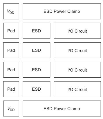
FIG. 9 Placement of ESD power clamps
With scaling, the sensitivity of the circuits has increased, requiring a lower impedance through the ESD Kirchhoff current loop. This increases the requirement for a lower power rail impedance in order to maintain a constant impedance through the ESD Kirchhoff current loop. As the power rails are separated into smaller domains, the ESD Kirchhoff current loop is limited to a smaller chip region, increasing the effective chip capacitance and the impedance.
To improve the effectiveness of the ESD Kirchhoff current loop, ''ESD rail-to-rail'' networks are placed between the power rails (e.g., chip substrate VSS and I/O VSS) to lower the effective impedance. In the case where no ESD rail-to-rail clamps are placed in the network, the system will find an alternative current path, which is the lowest impedance path (which may not be favorable). Additionally, the ESD testing results will be significantly lower or destruction of structures or circuits is possible. By placement of the ESD rail-to-rail networks in the system, the current flow can be directed through specified current paths.
ESD rail-to-rail networks provide electrical connectivity to nodal points in a system to allow the current flow from node to node but, at the same time, not to impact the noise requirements. Whereas the functional objective of the system is to minimize noise using both spatial and electrical separation, the ESD rail-to-rail network plays the role of reestablishing electrical connectivity during ESD events (FIG. 10).
These ESD networks are typically bi-directional in nature. This is to allow the current flow between the rails in either direction. The ESD rail-to-rail networks can be the networks where the electrical bias potential may be equal or unequal. ESD rail-to-rail networks can be voltage-or frequency-triggered elements.
For example, a typical ESD rail-to-rail network is a bi-directional string of diode elements (FIG. 11). The number of elements in series is a function of the noise margin and voltage differential between the two rails. The size of the diode structures is a function of the desired impedance needed for the ESD Kirchhoff current loop to allow the ESD current to flow to the isolated power rail. In digital design, the voltage differential may establish the number of series elements desired. In analog and radio frequency (RF) design, the capacitance coupling may determine the number of desired elements and the physical size of each diode element.
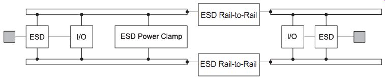
FIG. 10 ESD rail-to-rail protection integrated into multi-rail chip
design architecture.
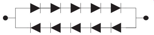
FIG. 11 Example of a ESD rail-to-rail network
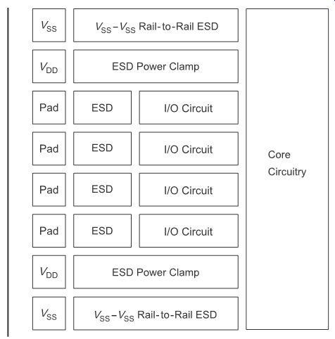
FIG. 12 Peripheral input/output (I/O) floor plan
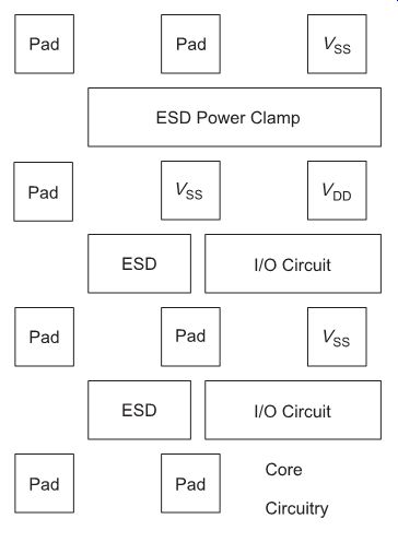
FIG. 13 Array input/output (I/O) floor plan
6.1 Placement of ESD Rail-to-Rail Networks
In the floor-plan of the system or semiconductor chip, the placement of the ESD rail-to-rail network can be a function of the impedance characteristics or architecture and floor plan of the semiconductor chip. The location of the signal pin, the nature of the distributed power plane, and ESD rail-to-rail element are contained in the ESD Kirchhoff current loop.
6.2 Peripheral and Array I/O
In establishing the floor plan for the semiconductor chip, the ESD design architecture must be considered for the peripheral and the array foot print I/O planning. Figures 12 and 13 are examples of the peripheral and ''array'' I/O circuitry. There are key distinctions in the ESD design synthesis for the two different floor plans.
In peripheral I/O design, the fundamental features have certain ESD design advantages; these are as follows:
_ Wire bonds and the I/O pads are placed on the chip periphery.
_ Wire bond pad area can be utilized for ESD structures under the pads.
_ ESD elements are placed local to the wirebond pad.
_ ESD element can be placed local to the I/O pad circuit.
In the case where the ESD element and the receiver circuit are separated spatially, this can lead to CDM concerns.
_ Adjacent pads can utilize ESD ''diode sharing'' and dummy metal rails.
_ Guard rings can isolate the ESD and I/O circuits from the interior latchup sensitive circuits.
_ ESD power clamps can be placed under power pads local to the I/O pads.
_ ESD Rail-to-Rail clamps can be placed under the power pads local to the I/O pads and power rails.
_ Power bussing for the ESD and I/O can be placed around the periphery of the semiconductor chip.
_ Substrate ground guard ring exists on the semiconductor chip substrate, providing a good substrate ground.
_ Power bus ground for ESD and I/O can be placed around the periphery of the semiconductor chip.
_ Electrical wire connection between the pad and the ESD device is not density or wire track nor wire-scaling limited.
_ External latchup sensitivity associated with the ESD network, I/O network, and its interaction with internal circuitry can be reduced with guard rings and physical spatial separation.
In an array I/O design, the fundamental features have certain ESD design advantages and disadvantages; these are as follows:
_ Circuitry exists under the pad regions. There is no ''structure under pad'' restriction.
_ ESD element are placed local to the I/O pad circuit within the I/O book.
_ Guard rings can be placed within the I/O pad book. Latchup is a greater concern in this architecture.
_ ESD power clamps and rail-to-rail circuits must be placed in a service module for every grouping of I/O circuits.
_ ESD rail-to-rail clamps must be placed in a service module for every grouping of I/O circuits.
_ Power bus for the ESD and I/O can be placed as a ''grid'' lowering the total bus resistance distribution problem that occurs in peripheral I/O bus. This lowers the resistance between any I/O pin and the ESD power clamps, as well as the voltage distribution across the entire chip.
_ Substrate ground guard ring exists on the external part of the chip, as well as internal substrate contact distribution.
_ Power ground bus for the ESD and I/O can be placed as a ''grid,'' lowering the total ground bus resistance distribution problem; this lowers the resistance between any I/O pin and the ESD power clamps, as well as the voltage distribution across the entire chip.
_ Electrical wire connection between the pad and the ESD device is density or wire-track or wire-scaling limited; this leads to interconnect failure as a major ESD failure mechanism in high-pin count semiconductor chips.
_ External latchup sensitivity associated with the ESD network, I/O network, and its interaction with internal circuitry can be a key concern. This can occur from voltage or current perturbations. HBM, machine model, and cable discharge events (CDE) can lead to latchup in array environments (FIG. 14).
_ External noise injection from the I/O network and its interaction with internal circuitry can be a key issue.
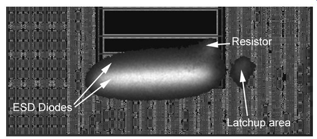
FIG. 14 Example of latchup problem from array I/O due to ESD networks
7. GUARD RINGS
Guard rings are used in semiconductor chip design to isolate circuits and circuit functions. Guard rings serve multiple roles in semiconductor chip design. Guard rings can be used to separate different types of circuits, and digital, analog, and RF circuit functions. Digital circuits serve as noise sources to analog and RF networks; hence, the isolation by separate power domains and guard rings is critical. Guard rings serve as good electrical contact regions, absorb minority carriers, and establish spatial separation between the noise source and the sensitive region. Guard rings can avoid parasitic pnpn devices between the different types of circuits (e.g., inter-circuit parasitic pnpn).
Guard rings are used to separate different circuit function. Guard rings isolate peripheral circuits from core circuits. Peripheral circuits, such as ESD networks and I/O OCD, can serve as a source of minority-carrier injection and noise. Adding guard rings serves in collecting the minority-carrier injection and serves as a ground shield. The effectiveness of the guard ring to collect minority carrier is a function of the ''guard ring efficiency.'' Guard ring efficiency is a function of the type of guard ring (e.g., n-well, p+ substrate contact, deep trench), the depth and width, and the underlying substrate properties.
Guard rings are also used within a circuit or sub-circuit to avoid latchup (e.g., intra-circuit parasitic pnpn) (FIG. 15). To avoid CMOS latchup in I/O OCD networks, guard rings are used between p-channel MOSFETs and n-channel MOSFET, which can form parasitic pnp, and npn devices, respectively. The inter-coupling of the pnp and npn forms an intra-circuit parasitic pnpn leading to CMOS latchup.
CMOS latchup can occur between two I/O cells, or between the ESD network and an I/O network. As a result, placement of the guard rings minimizes spatial and electrical coupling between ESD networks and I/O networks, which can lower the concern for CMOS latchup.
Guard rings can also be integrated into the ESD design. For example, they can be used as part of the ESD design to achieve discharge to the substrate or to the power rails. In this case, the guard ring can serve as a guard ring and ESD function (FIG. 16).
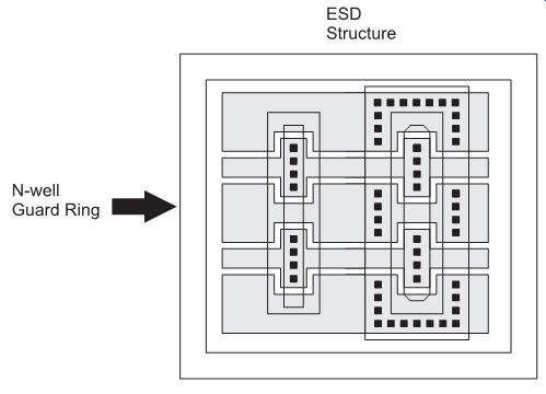
FIG. 15 Guard ring structures
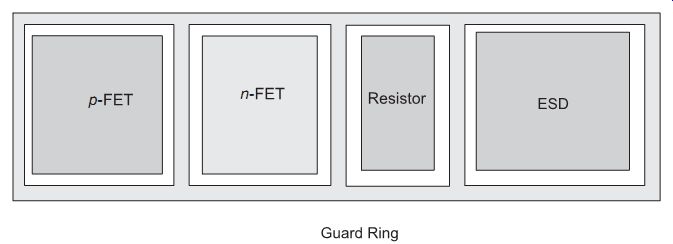
FIG. 16 Example of guard rings integrated into the ESD design
8. PADS, FLOATING PADS, AND NO CONNECT PADS
In the design and floor planning of systems and semiconductor chips, the ''foot print'' (e.g., pad size, spacing, and pitch) of the pads is defined not by the circuits in the chip but by the packaging or design system for compatibility. In this environment, there are cases of floating pads, unused, or ''no-connect pads.'' The footprint and placement of these pads can lead to ESD concerns. These structures are metal shape that can be charged from semiconductor wafer processing, human sources, shipping, or test equipment. These unused pads can be covered with an insulator film, exposed metal shape, or have solder balls. The solder balls are placed as mechanical supports but are not electrically connected to any circuits or power rails. In the case of source of current or charging of these elements, the voltage increases on the structures. As they charge, when the dielectric voltage is exceeded, inter-level dielectric (ILD) insulator failure occurs, leading to either cracking, insulator melting, or metal filling of the material defect.
As a result, the placement of signal lines, power busses, and the floor plan of these relative to the floating or ''no-connect'' pads can influence the failure mechanisms that can occur. Hence, the lack of electrical connectivity to the system and its spatial placement are critical to the success or failure of the usage of ''no connect'' structures.
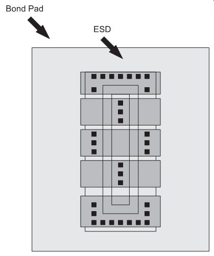
FIG. 17 Structures under pads
9. STRUCTURES UNDER BOND PADS
In the floor plan and design of a semiconductor chip, the area on a chip for different circuit function is established by chip function. ESD signal pin, ESD power clamps, and ESD rail to-rail devices can consume chip area, which is not insignificant. The area consumed by the ESD devices is a function of the number of logic circuits (e.g., Rent's rule). The area includes the number of signal pins, the number of power pads (e.g., VDD, VSS), and the size of the ESD networks. To reduce the area impact, area that are not used for functional applications can be utilized for ESD networks. These areas can include areas under the bond pads, between the bond pads, the corners of the chip, ''fill areas.'' ESD structures can be placed under bond pads to minimize the area impact to the chip. For peripheral signal pads, the I/O cells are placed near the periphery of the semiconductor chip. In this case, the architecture of the chip lends itself to allow the ESD networks under the pads. The floor plan of the semiconductor chip would involve allowing the ESD network under the bond pad and subsequently be connected to the peripheral circuit. This also lends itself to allow the ESD rail-to-rail networks under the power pads. In this architecture, the ESD networks are located on the outside of the chip, followed by the peripheral circuit, and then the core circuitry.
In many technologies, structures under bond pads (also known as circuits under pads) can lead to mechanical dielectric cracking, bond pad adhesion issues, and failure during humidity and temperature stressing. The success of the ability to place semiconductor devices under bond pads is a function of the dielectric material, the thickness of the dielectric materials, the metallurgy material properties, and the physical design. Because of the technology issues, the type of the ESD device, and the interconnect and wiring design can be influenced by the requirements (e.g., metal line width, metal-to-metal spacings, and the allowed metal level) (Figures 17 and 18). In today's technologies, there exist both aluminum and copper interconnects for the metal levels. Additionally, there are both silicon dioxide and low-k materials on the same and different levels. As a result, the qualification of ESD structures under pads must address different material mechanical properties.
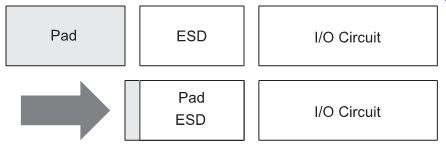
FIG. 18 Examples of an I/O book with pad over part of I/O cell
10. SUMMARY AND CLOSING COMMENTS
In Section 2, a brief overview of the elements to construct ESD protection was discussed:
ESD input circuits, ESD power clamp circuits, ESD rail-to-rail circuits, guard rings, and pad structures. The inter-relationship of electrical and spatial phenomena was discussed to provide the reader an understanding that one must think about both these aspects concurrently in the floor-plan and architecturing of ESD in a semiconductor chip. Addition ally, the relationship of noise, latchup, and ESD is briefly discussed, with the objective of making the reader conscience that other phenomena must be addressed in establishing the ESD design architecture and synthesis.
This provides a top-down perspective in developing an ESD strategy for a semiconductor chip. These will be discussed in depth in the following Sections; but first, spiraling downward, a bottom-up approach will be taken, starting from the basic design elements of MOSFETs, diodes, resistors, and other physical elements-then return to the elements discussed in this Section.
In Section 3, the layout and design of MOSFET devices are discussed. The MOSFET device is used in core and peripheral circuits, as well as in ESD networks and ESD power clamps. The design and layout fundamentals associated with designing MOSFETs are fundamental to the understanding of establishing ESD protection in NMOS, PMOS, CMOS, RF CMOS, and BiCMOS technologies.
PROBLEMS
1. Given a square semiconductor chip with signal pads and power pads on the periphery of the chip, of width W, pitch P, and chip size Wchip. Assume the maximum wire width from the signal pad to the ESD network is W/2. What is the maximum number of signal pins N, assuming a power pad is needed for every four signal pins? At what pad density will the wire interconnect failure occur below 4000 V HBM, assuming the wire achieves 500 V/mm?
2. Given a square chip with peripheral pads (as stated above), assume a metal bus runs across a double-diode ESD networks with a diode series resistance Rd. Assume a metal bus resistance signal pad to signal pad of R. Assume an ESD power clamp in each corner of the semiconductor chip. Plot the total resistance from all signal pads to the ESD power clamp including the diode series resistance and bus resistance. Derive the relationship as a function of chip size.
3. Given a square chip with peripheral pads as above, but assume a power pad (with an ESD power clamp in each power pad) is placed within the signal pads where the ratio of power to signal pads is fixed for a given design. Derive the resistance relation for each pad to each power clamp, as a function of the ratio of power to signal pads.
4. Given a square chip of edge WC, and array of pads whose pads are in an M x M array, where the total number of pads is N = M x M, and are on the last level of metal, LM.
Assume the metal level, LM-1, under the metal pads has a width W. Assume each successive metal level is scaled according to the MOSFET scaling parameter alpha.
Assume the interconnect from the LM-1 level connects from the pad to the ESD network and I/O cell. Assuming a minimum wire width, what is the width of the metal level for a LM-1 level? Assuming the first-level metal M1 fails from ESD events at a value V0 (in terms of HBM voltage), when does the successive levels fail at? How do these results compare to a peripheral signal pin result where the metal from the pad to the ESD is W/2 of a first level metal M1 material?
5. Given an I/O bank of OCDs, where the ESD network is integrated within the I/O cell, given a fixed I/O form factor of width W and length L. Assume the metal line connecting the I/O bank are in a wiring bay of fixed pitch associated with the I/O width W. At what I/O width, assuming 500-V HBM per unit micron of wire width will the chip not achieve 10-kV HBM? 8-kV HBM? 6-kV HBM? 4-kV HBM? 2-kV HBM? Assume the width and space between adjacent lines are equal for each I/O cell.
6. OCD bank ESD results can degrade along a chip design when the metal bus is not properly terminated. Given a bank of N OCD in series on a single metal VDD bus.
Assume that the bus is electrically connected to the chip power on one side. Produce an incremental model showing the ESD resistance and the bus resistance of the successive OCD cells. Assume a width W for the width of the OCDs, and a wire resistance R between each successive driver. Derive the anticipated ESD roll-off that occurs in the OCD bank for an assumed failure mechanism assuming an ESD current I. Make an assumption on the circuit type and failure mechanism in that circuit.
7. Assuming that ESD structures are placed under a pad. Given a square chip of edge W, square pad width Wpad, pad pitch P (pad and space), and square ESD devices of size WESD. Assume a core chip square area of WCORE is needed for circuitry. Derive a relationship of the number of pads for a given chip size, as a function of the variables above. Evaluate the total chip area savings when the ESD device is placed under a pad where the ESD area and the pad sizes are equal in magnitude. Given a 200- and a 300 mm wafer, what is the productivity improvement?