AMAZON multi-meters discounts AMAZON oscilloscope discounts
1. BASIC ESD DESIGN CONCEPTS
MOSFET ESD design contains many fundamental ESD concepts that are relevant to the MOSFET as well as to other structures. ESD design concepts address the control of MOSFET second breakdown, and the prevention of MOSFET dielectric breakdown.
These incorporate the concepts of sensitivity to ESD mechanisms such as human body model (HBM), machine model (MM), and charged device model (CDM) events.
MOSFET design must incorporate local to global effects from the contact to the multi-finger MOSFET structure. In this Section, we will focus on the MOSFET to highlight these issues.
In ESD design, there are some underlying fundamental concepts that one can adhere to in order to have effective ESD results:
_ Provide a solution that establishes a low-voltage trigger element, which can discharge a high current.
_ Provide spatially uniform current density within the trigger element.
_ Avoid localized Joule heating within the trigger element.
_ Avoid electrical connections that exceed the breakdown voltage of the dielectric films.
_ Operate the device under the MOSFET second breakdown voltage.
_ Improve thermal stability of the MOSFET structure.
The ability to provide a low-voltage trigger element can be achieved by the following means:
_ Minimum channel length MOSFETs to provide low MOSFET snapback voltages.
_ Low threshold voltage MOSFETs.
_ Gate coupling techniques.
_ Drain coupling techniques.
_ Substrate coupling.
_ Dynamic threshold MOSFET coupling techniques.
High current can be achieved in MOSFET ESD structures by the following means:
_ n-channel MOSFETs instead of p-channel MOSFETs for higher mobility (e.g., increased MOSFET current drive).
_ Low-threshold MOSFET for increased MOSFET current drive (e.g., maximize VG x VT).
_ Dynamic threshold voltage techniques.
Spatial uniformity is achieved in the MOSFET ESD structure by the following means:
_ Provide design symmetry in the metal and contact design.
_ Ballasting in the direction of the MOSFET current flow.
_ Ballasting perpendicular to the direction of the MOSFET current flow.
_ Segmentation of the MOSFET into multiple regions.
Avoidance of localized heating in the MOSFET structure can be achieved by the following means:
_ Provide design symmetry in the metal and contact design.
_ Ballasting in the direction of current flow.
_ Ballasting perpendicular to the MOSFET current flow (e.g., lateral ballasting).
_ Introduce internal ballasting elements.
_ Introduce external ballasting elements in the MOSFET ESD circuit.
_ MOSFET structures with deep junctions for increased emitter depth.
_ MOSFET structures with ESD implants (e.g., deep junctions) for increased emitter depth.
_ MOSFET structures with extension implants or deep low doped drain regions.
Avoidance of MOSFET second breakdown can be achieved by the following means:
_ Avoid the ESD MOSFET from undergoing MOSFET snapback.
_ MOSFET gate coupling techniques.
Avoidance of failure of the MOSFET structure due to dielectric breakdown can be achieved via the following means:
_ Avoid MOSFET gate-to-power rail direct connections.
_ Avoid MOSFET gate-to-pad direct connections.
Ballasting can be introduced in a MOSFET structure using the following ESD design methods:
_ Removal of refractory metal silicides on the MOSFET source and drain regions in the direction of the MOSFET current flow.
_ Removal of refractory metal silicides on the MOSFET source and drain region lateral to the MOSFET current flow.
_ Removal of silicide under contact regions.
_ Maintain high-resistance phase state of the silicide film (e.g., titanium has two resistive states).
_ Introduction of resistor elements in series with the MOSFET structure (e.g., n diffusion, p- diffusion, n-well, polysilicon film, tungsten local interconnect, and wire resistors).
_ Segmentation of MOSFET into multiple source and drain by introduction of isolation perpendicular to the MOSFET source and drain region.
_ Segmentation of MOSFET by introduction of lateral high resistance source and drain regions.
_ Segmentation of p-well and n-well regions by introduction of lateral well resistance regions.
Under high-current operation, the MOSFET undergoes electrical and thermal breakdown.
Second breakdown is an electro-thermal effect typically leading to thermal runaway and component failure. Parasitic bipolar transistors are inherent in bulk and silicon-on-insulator (SOI) MOSFET devices in parallel with the surface channel MOSFET conduction.
In a MOSFET, the current flow from the drain to source. In parallel with the drain and source diffusion, a parasitic bipolar transistor is formed. The total drain current can be expressed as a function of the MOSFET drain-to-source current, the parasitic bipolar current, and the thermal generation current,
The parasitic bipolar transistor can express the current in the form, ...
The base current can be expressed in a similar form where current is a function of the excess charge in the base divided by the recombination time,
In the case of a MOSFET, the base region is the p- substrate region. In the base, it can be assumed that the doping concentration in the lateral transistor structure is a constant. This simplifies the collector current equation.
...where Ae is the emitter area, Dn is the electron diffusion coefficient in the channel region, Na is the doping concentration in the channel region, and Leff is the lateral bipolar base width of the lateral npn which is the effective channel length. For a MOSFET, the emitter area is equal to the product of the MOSFET channel width and the source/drain implant junction depth, Weffxj. The effective area is the area that participates in the forward bias injection into the substrate.
For the base current, the equation can be expressed as...
...where the base current term I0e is expressed as...
The bipolar current gain is obtained from the ratio of the collector current to the base current. In the case of forward active voltage, the exponential term for the collector-base is negligible, and the bipolar current gain can be expressed solely as a function of the ratio of …
…the two current expressions.
This can be expressed as…
From the current model, avalanche generation can be expressed as a function of the multiplication factor and the total current flowing through the high-electric-field region, where the generation current can be expressed as…
When the electric fields are low, M is unity, leading to no generation occurring. As the electric field increases in the transistor, avalanche multiplication increases leading to the gene ration term. In this expression, some of the hole generation current will serve as base current for the lateral bipolar element, while some of the holes generated will enter the substrate serving as substrate current. The substrate current can be expressed as,
The substrate current in a MOSFET is typically an issue for hot electron generation and total power consumption. For ESD analysis, the substrate current is important because it is associated with the voltage drop that occurs locally in the MOSFET region at high currents
hence, the voltage drop in the substrate can be expressed as...
When the voltage drop equals the forward bias voltage of the p-n junction formed between the source and the substrate, MOSFET snapback occurs. This can be stated as,...
...or a condition for MOSFET snapback occurs when...
From this development, it is important to quantify the substrate resistance in order to anticipate the onset of MOSFET snapback. In a multi-finger structure, the MOSFET can be represented as a plurality of parallel MOSFET devices where the gate and the drain are coupled to common nodes, and the sources are independent nodes. The MOSFET fingers are also coupled together through the substrate potential drops. This introduces a complex model for the substrate current and the substrate resistances. This can be addressed through coupled system of equations, matrices, or transfer resistance representations.
In MOSFET devices, avalanche breakdown occurs in the metallurgical junction formed between the MOSFET drain and its supporting structure. In the case of an n-channel MOSFET, avalanche breakdown occurs in the n+ source/drain implant to p- epitaxy (e.g., or p- substrate) metallurgical junction. From the Townsend criteria,...
...where the integration of the impact ionization over the physical space where there exists a non-zero electric field. From this form, the avalanche multiplication factor M can be related to the impact ionization coefficient integrated over the depletion width and can be expressed as
In a depletion region, the peak electric field is maximum at the center region of the dipole.
In the analysis of the MOSFET, the model is simplified to express it as a function of the depletion width. Hence, it can be integrated over the integral and stated in the form
From semiconductor physics, it is known that the depletion width can be expressed as a power of the applied voltage
The power of this relationship is a function of the doping profile at the metallurgical junction. In this form, it is also clear that when the voltage is greater than the avalanche breakdown voltage, the multiplication factor should increase rapidly. Hence heuristically, it is clear that the multiplication expression should satisfy the form...
In this form, as the drain voltage approaches the avalanche breakdown voltage, the multiplication factor approaches infinity. Amerasekera pointed out that the above relation ship does not address the effect of the gate voltage on the electric field in a MOSFET gated diode region. As the gate electrode voltage in a MOSFET is increased, the electric field in the drain region increases. From the expression...
Substituting in a voltage condition where the electric field is the voltage over a physical distance, where the voltage across the depletion region is the drain voltage minus the drain saturation voltage, and the distance is the depletion region…
...where the drain saturation velocity is expressed as…
where saturation velocity is the voltage drive divided by a two-parameter expression in the denominator, and the voltage drive is the gate voltage minus the MOSFET threshold voltage.
The avalanche generation current can then be calculated from multiplication factor and the current flowing through the drain junction. The current flowing through the drain structure is the MOSFET current flowing through the surface region (e.g., MOSFET source to-drain current) as well as the current flowing from the parasitic bipolar transistor formed from the MOSFET source, epitaxy region, and the MOSFET drain forming a lateral npn transistor. In this case, the MOSFET drain and source serve as the bipolar junction transistor collector and emitter, and the epitaxial region serves as a base. The avalanche current can be expressed as…
The avalanche generation current flows to the p- substrate region of the n-channel MOSFET structure. A portion of this current flows to the base of the lateral parasitic npn transistor serving as the emitter-base current, while the rest of the current will flow to the substrate region as substrate current. Hence, the avalanche current can be defined as the sum of the substrate current (flowing to the substrate contact), and the base current of the lateral npn transistor (serving as base drive current)…
Then the substrate current can be estimated as…
From this expression, Amerasekera noted that the avalanche current and the substrate current can be expressed as a function of the impact ionization, the depletion width, drain voltage, drain saturation voltage, and MOSFET n-channel and parasitic npn current.
1.1 Channel Length and Line width Control
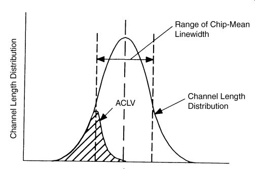
FIG. 1 Line width
In the ESD design of a MOSFET structure, the MOSFET channel length has a key role. The MOSFET channel length has a role in the MOSFET snapback voltage and the MOSFET dynamic on-resistance. On a local scale, the MOSFET channel length and the MOSFET line width control have an important role in the current distribution in multi-finger MOSFET structures. On a global level, the MOSFET across-chip line width variation (ACLV) has an influence on the ESD failure pin probability distribution and cumulative failure distribution functions (FIG. 1).
The understanding of the MOSFET channel length control plays a role in the ESD response of single-finger and multi-finger MOSFET structures. On a local scale, the MOSFET linewidth control has an important role in the MOSFET snapback voltage and the current distribution in multi-finger MOSFET structures. In a multi-finger MOSFET structure, the relative channel lengths play a role in how the current distributes in the MOSFET structure. On a global level, the MOSFET ACLV has an influence on the ESD failure pin probability distribution and worst-case pin failure. The MOSFET channel length and the channel length linewidth control is a function of the MOSFET photolithography, MOSFET gate stack structure, and the MOSFET gate etch process.
The scaling of MOSFETs has led to a significant evolution of the photolithography and gate conductors etching processes. Scaling of the numerical aperture (NA) and exposure wave length of lithographic systems from G-Line (436 nm), I-line (365 nm), deep ultra-violet DUV (e.g., 240 nm), and 193-nm lithography permitted technology scaling to sub-0.5 mm dimensions. Today, demonstrations of extreme-ultraviolet (EUV) micro-exposure tools at 32 nm have been demonstrated for 30-nm isolated lines. With the transition from LOCOS isolation to shallow trench isolation (STI) and the introduction of anti-reflective coating (ARC), topography issues that influence linewidth were reduced; however, new gate conductor linewidth issues were discovered that influence MOSFET design. MOSFET linewidth distribution is used to control semiconductor manufacturing assembly lines. At long channel lengths, channel length limited yield (CLLY) tends toward zero because of poor chip performance. At short channel lengths, yield tends to zero because of MOSFET channel length hot electron degradation, MOSFET device leakage, MOSFET punch-through, and MOSFET timing race conditions. These limitations have led to considerable amount of interest in gate linewidth centering, optimization, and control. Channel length control can be divided into two broad categories: chip-mean linewidth variation (CMLV) and across-chip linewidth variation (ACLV). Both CMLV and ACLV influence the ESD failure distribution and ESD robustness of an individual semiconductor chip. CMLV and ACLV both determine the channel length variation, _L. CMLV consists of across-wafer components, wafer-to-wafer, and lot-to-lot variations. CMLV is calculated as the root-mean-square variation of the lot-to-lot, wafer-to wafer, and chip-to-chip variation. This distribution contains both systematic and random variations. Each variation can be driven by different production issues. Chip-to-chip variation, for example, can occur due to tool radial distributions of etch processes.
Wafer-dependent lithographic variations can determine wafer-to-wafer linewidth control variations. The chip mean linewidth distribution is a function of how a manufacturing line is controlled and a tool set quality. On the other hand, ACLV component, the within-chip linewidth variation, is driven by the local lithographic and gate-conductor etch processes.
For large chips, systematic and random mask variations, lens distortion, and photo tool slit intensity variations play a role in the across chip variations. ACLV includes systematic effects associated with variations in the x-y orientation (e.g., astigmatism and comma), identical and non-identical lines, gate-to-gate spacing (e.g., gate pitch), and within-chip spatial variations. ACLV also contains etch-loading effects: aspect ratio-dependent etching (ARDE), micro-loading, and macro-loading. For ARDE, etch bias is dependent on adjacent structures. Micro-loading occurs where etch bias for identical structures varies as a result of local pattern density factors. Macro-loading reflects the etch-bias differences created by average etch loading on a wafer.
CMLV and ACLV are treated as two separate and independent parameters. For ESD analysis of semiconductor chips, these two parameters should be considered as separate issues. In the case of CMLVs, this impacts the ESD robustness chip-to-chip. Given that the MOSFET linewidth influences the ESD robustness of the technology, this will influence the ESD variation of tested product and will influence the sample size to guarantee the worst case ESD robustness. From a design perspective, the ACLV issue is a larger concern in which it influences the ESD variation within a MOSFET, the pin-to-pin ESD failure probability distribution, and the worst-case pin condition.
1.2 ACLV Control
Controlling across-ACLV is one of the most important variables in semiconductor chip development, and can play a key role in ESD design practices for single finger and multi-finger MOSFET design. ACLV is important for circuit functionality, circuit-to-circuit matching, standby power, and MOSFET hot-electron degradation. ACLV is a function of both etching and photolithographic bias. Etching bias variability is defined as the difference between a photo-resist and etched critical dimensions. Etching and photolithographic bias variability are the two dominant components in ACLV control. ACLV consists of both local and non-local effects from both photolithography and gate conductor etching. The non-local systematic and random effects influence the ESD pin distribution, when the MOSFET channel length is the dominant ESD-limiting result. The local systematic effects influence the MOSFET design layout and the ESD robustness of a given single- or multi-finger MOSFET structure.
Parameters that are key to ACLV are:
_ Line-to-line matching of two adjacent lines.
_ Orientation.
_ Nesting effects.
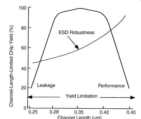
FIG. 2 Linewidth distribution and ESD
FIG. 3 Difference between an isolated and nested line bias as a function of design pitch
Photolithographic chip field variations influence the MOSFET channel length of two identical MOSFET transistors with the same orientation, at two different locations in the optical field. This non-local macroscopic effect of chip field variations leads to a wider ESD pin distribution. Lens distortion, such as astigmatism and coma, can lead to x-y orientation dependent effects. ACLV measurements of identical MOSFET structures, which are oriented on a different axis, have different channel length distributions. The x-y orientation is relevant to semiconductor chips with peripheral I/O books, which contain I/O off-chip drivers and ESD elements, whose orientation changes around the semiconductor chip. In the choice of the floor plan, the orientation of the MOSFET-based off-chip driver (OCD) circuits and ESD elements changes on two sides of the chip. Therefore, ESD pin distributions are widened by this issue. In the peripheral I/O floor plan, the ESD pin distribution samples both the full chip field variations and the x-y orientation issues.
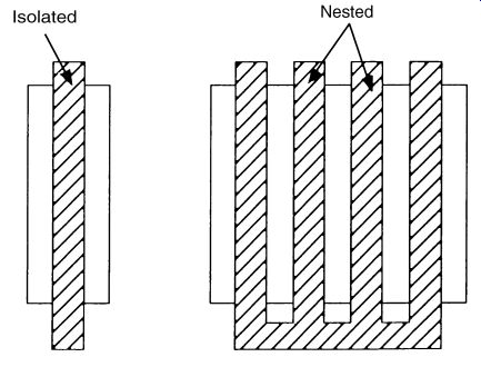
FIG. 4 Example of an ''isolated'' and ''nested'' MOSFET image
For local ACLV effects, the ''nesting'' phenomenon is of significant importance to the ESD design of single- and multi-finger MOSFET structures. Linewidth control in the diffraction limit of photolithography tools for minimum images leads to linewidth bias, which is dependent on both the gate conductor length and space to the adjacent gate conductor. Linewidth bias occurs when the relative difference between the maximum and minimum intensity is modulated by the spacing between the adjacent intensity peaks. For positive tone resist, as the space between the two identical gate conductor lines decreases, the linewidth bias increases. For negative tone resist, linewidth bias decreases with decreasing gate-to-gate space. This effect is the result of the differences in the resist exposure in the optical diffraction limit. Hence, depending on the photo-resist, opposite effects can occur as a function of the linewidth gate-to-gate space. For the etch process, with etching complex gate structures, several sequential plasma etching steps are required leaving behind sidewall passivation and polymer build-up. Aspect ratio-dependent etching dominates the linewidth variation as a function of the gate-to-gate space.
Linewidth control influences the ESD robustness of a multi-finger MOSFET. FIG. 3 shows the linewidth difference as a function of the MOSFET gate pitch (e.g., sum of the MOSFET gate length and gate-to-gate space). As the pitch decreases, the linewidth variation difference between ''isolated'' line and the closely spaced ''nested'' line rapidly decreases. FIG. 4 shows an ''isolated'' and ''nested'' MOSFET image. An ''isolated'' line is a gate conductor with no parallel adjacent gate structure within some distance (e.g., gate-to gate space greater than 10 mm). As the spacing increases, the photo and etch bias change decreases, providing a fixed linewidth ''isolated line.'' A ''nested'' line is a MOSFET gate structure with an adjacent parallel gate structure within a given distance (e.g., gate-to-gate spacing less than 10 mm). As the pitch decreases, the ''nested-to-isolated'' bias increases. For positive tone resist process, the ''nested-to-isolated'' etch and the photolithographic bias are additive. For negative tone resist process, the ''nested-to-isolated'' etch and photolithographic bias are subtractive.
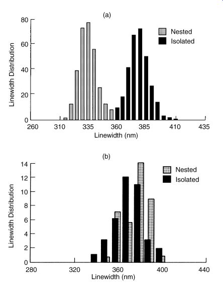
FIG. 5 (a, b) Positive and negative tone resist linewidth distributions
for isolated and nested MOSFET gate structures
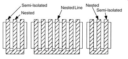
FIG. 6 MOSFET driver pull-down polysilicon level and source/drain region.
The MOSFET is segmented for improved slew rate control
Linewidth metrology can determine the linewidth structure. For characterization of the MOSFET linewidth, four-point probe resistor structures with ''dummy lines'' are measured.
To evaluate the change in the linewidth, the linewidth and pitch can be varied to understand the dependency. In FIG. 5, linewidth distributions were determined using isolated and nested structures for the positive and negative tone processes.
The ''nested-to-isolated'' effect also influences the MOSFET gate conductor sidewall slope. The MOSFET sidewall slope influences the MOSFET effective channel length, and hence the MOSFET snapback voltage. Gate conductor sidewall variations can alter MOSFET second breakdown by influencing the MOSFET source and drain implant profiles in the MOSFET overlap region. The gate conductor sidewall profile is also affected by ARDE, micro-, and macro-loading effects. Using two-dimensional atomic force microscope (2-D AFM) metrology techniques, the sidewall slope can be accurately measured. As the MOSFET gate-to-gate spacing increases, with positive tone resist, the MOSFET sidewall slope decreases. Hence, isolated structures will not only have a higher MOSFET channel length, but will also have a more gradual MOSFET drain doping profile.
As an example, an application of a MOSFET OCD network contained an n-channel MOSFET pull-down device. The MOSFET pull-down was separated into three segments.
During functional operation, to control slew rate, the three segments were driven at different times. The gate structure consisted of a first three-finger MOSFET gate structure, a multi-
finger MOSFET gate, and a second three-finger MOSFET gate structure. FIG. 6 shows a picture of the MOSFET OCD gate structure.
Measurements of the MOSFET polysilicon fingers show that the edge lines of the three-finger MOSFET stages were 0.01 mm larger than the center line. In the ESD measurements, failure analysis consistently showed that the MOSFET failure occurred in three locations.
First, the center fingers of the two three-finger structures consistently showed ESD damage during HBM testing. The location of the MOSFET second breakdown damage always occurred in the center finger of the three fingers (FIG. 7). In the case of the larger multi-
finger center structure, damage was typically contained within one of the center fingers in the seven-finger structure, but never the edge MOSFET polysilicon fingers of the center stage.
Hence, although many other design features are of concern in ESD MOSFET design, in this implementation, the dominant failure mechanism was driven by the MOSFET ''nested-to isolated'' issue.
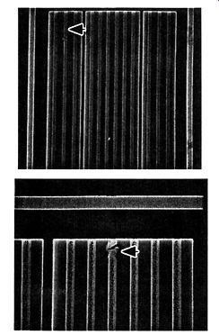
FIG. 7 Failure analysis of MOSFET with systematic MOSFET second breakdown
1.3 MOSFET ESD Design Practices
In summary, the MOSFET ESD and I/O design must note the following ESD design issues:
_ Orientation of MOSFET ESD elements and MOSFET-based OCDs may be dependent on the x-y orientation channel length, driven by optical lens distortion. This is most likely in peripheral I/O design.
_ Placement of MOSFET ESD elements and MOSFET-based OCDs on the periphery of the entire chip will be sensitive to optical chip-field variations.
_ Multi-finger MOSFETs are sensitive to ''nesting'' phenomenon; the MOSFET gate-to gate spacings and the ''nested-to-isolated'' linewidth variation impact the channel length matching of MOSFET channel lengths.
The following MOSFET ESD design practices can be instituted to provide better MOSFET finger linewidth matching:
_ Configure MOSFET OCDs in the same x-y orientation if possible to eliminate x-y lens distortion effects.
_ Place MOSFET OCDs and MOSFET ESD networks locally adjacent to provide improved across chip matching and reduce the effect of the full optical field.
_ Provide a fixed gate-to-gate spacing of MOSFET fingers in a given MOSFET network.
_ Use an even number of MOSFET polysilicon fingers instead of odd number of fingers (e.g., two instead of three).
_ Provide a MOSFET gate-to-gate spacing, which is not in the strong roll-off region of nested-to-isolated bias.
_ Place ''dummy MOSFET gate'' fingers on the edges to eliminate mismatch of the end gate structure to the nested MOSFET fingers.
_ Avoid semiconductor processes with high ''nested-to-isolated'' linewidth mismatch.
_ Use semiconductor processes where the MOSFET gate etch and photolithographic bias are subtractive.
_ Use thinner polysilicon gate structures (reduces ARDE issues).
_ Use negative tone resist instead of positive tone resist.
_ Linewidth metrology can be used for MOSFET ESD model development to accurately evaluate the relationship between the true linewidth and the MOSFET snapback condition.
2. ESD MOSFET DESIGN: CHANNEL WIDTH
2.1 n-Channel MOSFET Design: Channel Width
In ESD design, the MOSFET channel width is an important design parameter. The effectiveness of a MOSFET for ESD protection is a function of how the current distributes through the MOSFET structure. The effectiveness of a MOSFET for ESD protection associated with its width is a function of the following design parameters:
_ MOSFET source/drain lateral sheet resistance.
_ MOSFET silicide resistance.
_ MOSFET contact-to-contact spacing.
_ MOSFET metal resistance along the MOSFET width.
_ MOSFET finger width symmetry (similar or dissimilar lengths).
_ MOSFET substrate contact orientation relative to the MOSFET width.
_ MOSFET lateral ballasting design.
In the list above, the first four items influence the effective lateral resistance in the MOSFET structure along the MOSFET width. These parameters affect the MOSFET current constriction and the MOSFET second breakdown ESD metric of MOSFET current/unit width (e.g., at the MOSFET second breakdown). Additionally, the MOSFET finger width symmetry finger-to-finger influences the ESD failure. This is most apparent in programmable impedance OCD circuitry. Additionally, the orientation of the substrate contact and lateral ballasting technique influence the current distribution in the MOSFET.
3. ESD MOSFET DESIGN: CONTACTS
In ESD design, the microscopic and macroscopic interactions within a MOSFET structure influence the high current operation of a MOSFET. In a MOSFET structure, the placement of the physical contacts influences the ESD robustness. The placement of the MOSFET source and drain contact relative to the MOSFET gate locally influences the current distribution within the physical space. The MOSFET contact-to-contact spacing also defines the current uniformity at the MOSFET gate edge. The MOSFET contact-to-isolation can influence MOSFET leakage mechanism post-ESD stress. The MOSFET contact on the edge of the MOSFET can influence ESD failure mechanisms at the edges of the MOSFET structure.
3.1 Gate-to-Contact Spacing
The MOSFET contact-to-gate spacing locally influences the current uniformity within the MOSFET source and drain junctions. For MOSFET with refractory metal silicide, the current flows through the refractory metal silicide film from the physical contact to the MOSFET gate. Evaluation of the current density within the silicide film provides some insight into the local current distribution and spatial variation in the MOSFET structure.
Assuming a two-dimensional plane where the circular contact is placed on a silicide surface, a solution can be obtained.
Using the method of images, let us assume a source and sink at x = a and x =_a equally spaced from a virtual plane perpendicular to the source and sink. The x-direction is the direction toward the MOSFET gate structure. Defining a complex variable function,
Separating the real and imaginary parts, the complex number z can be represented as a mapping of two harmonic conjugate fields, which satisfy the Cauchy-Riemann equations, ...
Given the source and sink are line charges of a given charge density per unit length, of equal and opposite strengths, ) and _ , respectively, the density function can be defined as...
If we let the first conjugate harmonic field be a constant then the ratio of the first and second radius, r1 and r2, is a constant. This can be shown to produce a locus of points that prescribe a circle. Letting the function _ be a scalar potential field, the electric field can be represented as minus the gradient of the potential field. Since the natural mapping of this potential field produces circular potential contours, we can represent one of the equi-potentials as a contact with a given radius. Assuming a contact of radius R, we can find the equi-potential surface by finding a first and second point where the ratio of the radii is a constant. Let us define a spacing between the center of the MOSFET contact and the MOSFET gate edge as distance ''l''. We can now relate the original sink ''a'' to the MOSFET contact radius, R, and the distance between the center of the contact and the gate edge, ''l.''
[...]
From this expression, it is clear that the self-heating in the silicide film between the contact and the MOSFET gate structure is a function of the parameter k. The parameter k shows the relationship between the center point of the contact and the ratio of the contact size. Hence, the dimensional size of the physical contact and the spacing of the contact to the MOSFET gate structure influence the peak self-heating in the MOSFET structure.
Hence, in the ESD design of contact structures in MOSFETs, the following design parameter is ...
_ The ratio of the sum of the MOSFET contact-to-gate space and the contact radius over the contact radius is a key ESD design parameter in the MOSFET self-heating, where k is expressed as...
3.1.1 Off-axis current distribution
To determine the current gradient off-axis, the values off the y = 0 axis can be evaluated from the current equation. This is obtained by evaluating the derivative of current with respect to the variable y keeping the variable x a constant.
3.1.2 Self-heating equi-energy contours
To determine equi-energy contours, the general equation for self-heating can be set to a constant. Setting the expression equal to a constant, C, the solution for the equi-energy potential can be solved as a function of x and y. The solution forms a quadratic polynomial expression, which is quadratic in y2
…where K is a function of constant C, and expressed as…
In quadratic form, the expression can be converted into a canonical form if the coefficients were symmetric, but they are asymmetric. At the position where ''a'' is much greater than x and y (e.g., at the MOSFET gate edge), the second-order-form terms dominate leaving the approximate expression…
Near the center point, the locus of points of equi-energy can be expressed as a hyperbolic equation in canonical form. At large distances from the center, the fourth-order terms dominate, producing an equation of a circle,
Between the two limits, the locus of points that form equi-energy contours will be elliptical in nature.
In the MOSFET structure, in the region of self-heating, the local temperature is increasing. As the temperature in a titanium silicide film increases, transformations occur in the material properties. Hence in the region of high local self-heating, the silicide property will be altered during ESD events. Failure analysis of MOSFET devices after MOSFET second breakdown shows that the silicide between the MOSFET contact and the MOSFET gate structure changes thermal properties. Using a Wrights' etch, material, which has undergone material property changes due to self-heating, can be highlighted.
FIG. 8 shows an example of the contour patterns evident in the contact area. Regions of equi-energy contours that undergo heating will be highlighted in the etch process. The failure analysis demonstrates the elliptical equi-energy contours.
3.2 Contact-to-Contact Space Figure
8. Failure analysis of a MOSFET device
In ESD design, the local interactions within a MOSFET structure influence the high current operation of a MOSFET. The MOSFET contact-to-contact spacing also defines the current uniformity at the MOSFET gate edge.
Between each physical contact in series, there is a physical resistance associated with the metal bussing, the silicide film, and the contacts themselves. The metal bus, the row of contacts, and the diffusion resistance between form a resistive ladder network along the drain and source region. Each incremental section between each physical contact can be treated as a resistive transmission line, where the incrementation is defined by the contact-to-contact spacing.
On a local understanding, as was shown in the analysis of the contact-to-gate spacing, the relative distance between the centroid of the contact to the MOSFET gate, l, and the contact size (e.g., radius R)influences the local current uniformity.
From the analysis, the current in the x- and y-dimension,...
In the analysis, the current density is shifted relative to the axis of symmetry for each physical contact. When the contact-to-contact spacing is significantly larger than the contact to-gate and radius of the contact, each solution of the current density will appear independent. If we can assume linear superposition, the net current density along the axis will be the sum of the current source. As the spacing of the contact-to-contact become on the same scale as the contact-to-gate distance and contact radius, the current at the MOSFET gate surface will become more uniform.
From the above expression, we can normalize the solution to the parameter a, and the contact-to-contact space parameter b.
In the case of y = 0, it is clear that the solution can be put in the form of the ratio of the parameter a, and the contact-to-contact space parameter b. For example,...
Hence, the solution of the current density at x = 0and y = 0 from the contact at y = b is a function of the contact-to-contact space, the contact radius R, and the MOSFET gate-to-contact spacing. Additionally, the influence of the contact on its adjacent contact is a function of the ratio of a second ratio term, which we can refer to as k2...
As an ESD MOSFET design guideline, we can state the following:
_ A first ESD design parameter, which defines the current uniformity from a single contact, is associated with the gate-to-contact spacing, and the contact radius ....
_ A second ESD design parameter, which defines the current uniformity due to a plurality of contacts, is a function of the gate-to-contact spacing, the contact radius, and the contact-to-contact spacing, ...
_ A ESD design parameter, which inter-relates the two metrics, can be referred as k3 stated as:
During ESD events, as the contact-to-contact spacing decreases, the current uniformity along the MOSFET gate surface improves. In many applications, the contact-to-contact spacing is equal to the size of the physical contact at minimum pitch. If we define the contact-to-contact space as the center-to-center value, b, the physical separation is actually b x 2R. Hence, in practice, the distance between the two contacts is b x 2R that equals the diameter of the contact, or b x 2R = 2R,or b = 4R.
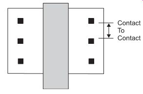
FIG. 9 Contact-to-contact
On a higher level, between each physical contact in series, there is a physical resistance associated with the metal bussing, the silicide film, and the contacts themselves. The metal bus, the row of contacts, and the diffusion resistance between form a resistive ladder network along the drain and source region. Each incremental section between each physical contact can be treated as a resistive transmission line. In a method by DeChairo and G. Krieger, the analysis is discussed as a resistive transmission line. In the higher order model, there are two resistance parameters, one representing the contact-to-contact resistance associated with the metal, diffusion, and silicide, and a second resistance parameter associated with the on-resistance of the MOSFET during conduction. In their analyses, a design parameter associated with the lateral resistance and the MOSFET device resistance solves the characteristic equation. In our analysis, a design parameter is present relating the dimensional similitude of the lateral spacing contact-to-contact, a series term of the contact to the MOSFET gate, and a third parameter, the contact size (FIG. 9). Note that the current density term is related to a resistance term, related to the local spreading resistance between a first point (source) and a second point (image sink) in a two-dimensional plane, where the first point has a finite radius.
3.3 End Contact
Placement of the MOSFET contacts near the end of the MOSFET structure can lead to MOSFET contact ESD failure due to high-current phenomenon from the semiconductor substrate region. Given a CDM event, current can flow from the substrate to the grounded node of the MOSFET structure. In the case of a grounded MOSFET gate structure, the current will flow through the MOSFET gate dielectric due to C (dV/dt) effects. In a CDM event where the MOSFET diffusion is connected to the grounded input node, current will flow from the chip substrate to the input node. In a receiver network, an n-channel MOSFET half-pass element will have one diffusion connected to the receiver and the second connected to the input pad. In this case, C. Duvvury stated that the current flowing laterally from the MOSFET drain structure will have a higher current density and flow to the first physical contact on the MOSFET drain [38]. In this case, the first contact in the substrate will obtain a higher current density than adjacent contacts leading to MOSFET failure (FIG. 10). This is analogous to the three-dimensional effect observed in p+ /n-well diode structures from positive polarity ESD events. ESD design practice to reduce this effect is as follows:
_ The MOSFET contact at the beginning and at the end of the MOSFET diffusions are spaced from the end of the physical diffusion at a greater distance than the minimum spacing.
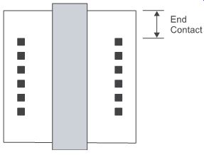
FIG. 10 MOSFET end contact issue
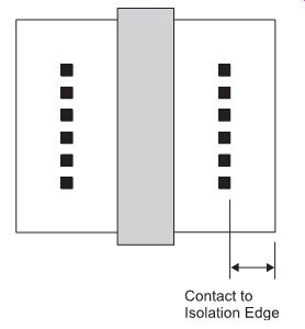
FIG. 11 Contact to isolation edge
3.4 Contacts to Isolation Edge
Placement of the MOSFET contacts near the MOSFET source and drain isolation structure can lead to reliability concerns. This is to avoid LOCOS isolation bird's beak and/or STI pull-down, influencing the MOSFET effective junction depth. The MOSFET contact is spaced from the MOSFET drain and source isolation edge to avoid the process sensitivity issues. As a conservative measure, the placement of contacts relative to the MOSFET source and drain isolation edges is spaced above a minimum design dimension.
ESD design practice to reduce the effect of contact-to-isolation effect is as follows:
_ The MOSFET contact is spaced from the MOSFET drain and source isolation edge (FIG. 11). This is to avoid LOCOS isolation bird's beak and/or STI pull-down, influencing the MOSFET effective junction depth and current crowding issues.
4. ESD MOSFET DESIGN: METAL DISTRIBUTION
4.1 MOSFET Metal Bus Design and Current Distribution
The layout design and resistances of a single- and multi-finger MOSFET have significant influence on the ESD robustness of the structure. Typically, signal pins, I/O pins, and output-only pins consist of large multi-finger MOSFET circuit elements, which are defined by the I/O foot print and pad-to-pad pitch. Additionally, ESD networks use multi-finger layout configurations. The current distribution through these elements have significant influence on the ESD robustness.
4.2 MOSFET Ladder Network Model
An early model analyzed this effect as a resistive ladder network. DeChairo assumed during avalanche breakdown that each MOSFET source-to-drain region can be analyzed as a simple single resistor element, R1. The resistor R1 represents the total resistance across a single-finger MOSFET structure from the drain to the source. In this model, it is assumed that the resistance value R1 is time invariant during an ESD event. In the ''comb'' structure, the metal routing from a finger-to-finger was assumed to be a second resistor R2 (e.g., the metal connection between each adjacent finger). FIG. 12 shows the multi-finger MOSFET represented as a resistive ladder network.
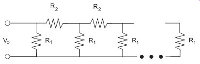
FIG. 12 Multi-finger MOSFET ladder network model
In this ladder network, the left-hand side (LHS) has a voltage source that supplies the incoming current to the distributed ladder network. In this model, the lower source connections is at the same electrical potential with no resistive elements on the lower part of the ladder network.
Using Kirchhoff's current law, the solution for the ith current loop can be solved as:
For N current loops, there exists N equations of this form. The set of N equations can be represented in a matrix equation form consisting of a generalized N x N resistance matrix, a current column vector, and a ''zero'' column vector.
R_ I = 0 where
In this matrix, the term 2R1 + R2 is on the main diagonal, and R1 is on the off-diagonal terms, which are adjacent to the main diagonal.
The solution to this matrix is achieved by defining two recursion coefficients Xj and Yj, which satisfies the relation ....
At the end of the ladder network, only the Nth and (N x 1)th current terms exist, simplifying the Nth loop equation to....
Once the boundary condition is established for the (N x 1)th loop, the recursive coefficients can be solved for each of the current loop terms. This is achieved by re-substituting the recursive coefficient equation into the current loop equation.
The recursive coefficient equation can be substituted into the current loop equation for the ith loop. From this, a general expression for the recursive coefficient can be obtained...
In this double-recursive solution form, the current distribution through the network can be obtained. A key result from the analysis is that the recursive coefficients are a function of the first and second resistor values.
As a special case, let us assume that the finger-to-finger resistance R2 is significantly larger than on-resistance of the MOSFET device. Let R2 x R1 ...
From the boundary condition, the ratio of the two resistances plays a role in the characteristic solution; and the recursive coefficients can be approximated as (where again it can be observed that the ratio of the resistance plays a role in the solution).
Hence, the ratio of the resistance of the metal interconnect relative to the MOSFET device source-to-drain resistance (during ESD operation+ is critical to the understanding of how the current is distributed throughout the network. This fact is also apparent in the Krieger model of parallel and anti-parallel current flow within a single finger. The form and nature of the coefficient is a function of the assumptions used in the ladder network representation.
In the case that the value of resistance R is much less than R , then...
DeChairo established a metric expression to compare the performance of a single-finger MOSFET to the multi-finger implementation. Opening the comb structure where only current flows through the first element, the current can be expressed as…
With the full network connected, the difference in the resistance between a single-finger MOSFET and a multi-finger MOSFET can be evaluated as ...
DeChairo defined an ESD enhancement factor (EEF), where…
.......
The EEF metric expression is the enhancement of a multi-finger MOSFET over a single-finger MOSFET. To quantify the ESD roll-off in the multi-finger structure, DeChairo evaluated different cases of the resistance ratio of the metal resistance to the n+ sheet resistance. In the case that the metal resistance approaches zero (e.g., R2 < < < R1), the ESD results with increasing structure size should increase linearly. In the opposite limit where the metal resistance is infinite, (e.g., R2 > > > R1), current does not flow into the multiple-finger segments beyond the first finger. In this case, as the number of fingers increases, the ESD results do not increase (i.e., they are independent of the number of fingers). In the limit that the finger-to-finger metal resistance approaches zero, the ESD results will increase in a linear fashion with structure size. In the case where the resistance of the metal is significantly higher than the MOSFET resistance, no increase in the ESD results occurs.
Hence, a design curve can be drawn of ESD failure results versus structure size, where the design box is constrained to a triangular region whose upper limit is the linear scaling line with structure size (e.g., MOSFET width) and the lower limit is the ESD failure result for a single-finger structure. Actual measurements will fall within this design curve region. In the design of a multi-finger MOSFET structure, the ideal case is to have the results approach the upper bound of the design box. As the ratio of the metal resistance to MOSFET source-to drain resistance decreases, the upper bound of the design box is approached.
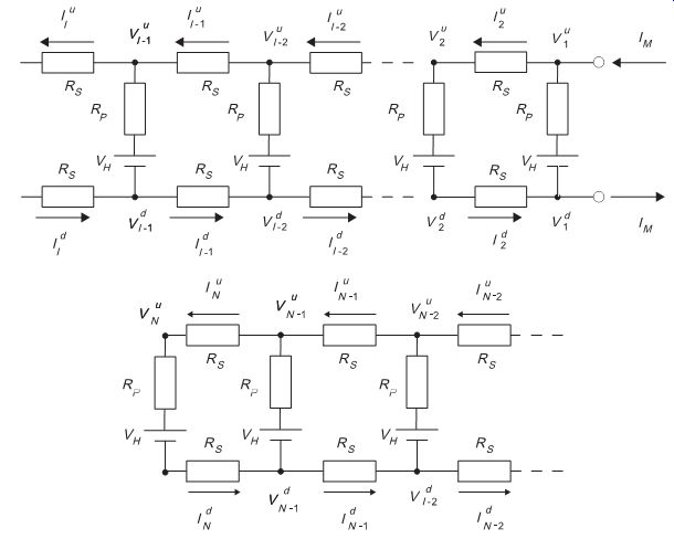
FIG. 13 MOSFET wiring with anti-parallel current flow
4.3 MOSFET Wiring: Anti-Parallel Current Distribution
In a MOSFET structure, the local distribution of the ESD current is strongly influenced by the metal routing. The metal routing influences which part of the MOSFET structure will undergo MOSFET snapback or MOSFET second breakdown.
During an ESD event, for example, the current flows into the MOSFET drain metal line, from MOSFET drain-to-source and out the MOSFET source metal line. The electrical connection to the MOSFET source and drain can be on the same or the opposite sides. In the case where the current is flowing in the same direction, it will be referred to as parallel current flow (e.g., enters and exits on opposite ends of the MOSFET structure). In the case, where the current is flowing in opposite directions, it will be referred to as anti-parallel current flow (e.g. enters and exits on the same end of the MOSFET structure) (FIG. 13).
An incremental model can be established that quantifies the voltage distribution within the MOSFET structure. Krieger proposed that we establish an incremental model, where each contact defines an electrical node and each region between each contact to be modeled as a resistor element. Krieger proposed to best understand the MOSFET during second breakdown; a distributed model is established based on the holding voltage, the dynamic-on resistance, and the metal resistance. During the MOSFET snapback, the MOSFET goes through an unstable negative resistance state and settles into the holding state. The holding state is the lowest voltage and lowest current point where stability is re-established. Krieger defined a network, where the lateral resistance between each physical contact can be defined as a resistor Rs. The MOSFET is represented as a voltage source VH (whose magnitude is the holding voltage) and a local term Rp, which represents the dynamic-on resistance Rd divided by the number of electrical nodes along the electrical network. In this fashion, the MOSFET structure is re-represented as a resistive ladder network with a voltage source between the upper and lower segments of the ladder network.
To solve for the solution of the voltage distribution in the MOSFET structure, the boundary conditions must be established. In the case of the anti-parallel current flow, we can establish a boundary condition that the metal lines are ''open'' on the left-hand side (LHS), and the electrical connections on the right-hand side (RHS) is the source of incoming current and outgoing current. For current conservation, the incoming current in the drain is equal to the outgoing source current.
In the network, it is assumed that the wire resistance of the MOSFET drain and that of source is equal in magnitude, and the contact density is the same. In this fashion, the MOSFET can be divided into equal segments on the upper and lower regions. Along the top and bottom of the network, the regions are segmented with resistors Rs. Between the upper and lower parts of the circuit network, they are electrically connected using resistor Rp and voltage source VH. Since the current flow is symmetrical for each incremental segment, Krieger noted that the analysis of the anti-parallel routing can establish a line of symmetry. A virtual line of symmetry is established, which divides the voltage source and the resistor by a factor of 2. This is analogous to the method of images, where an image is established around an equi-potential (FIG. 13). The equi-potential line of symmetry has a zero voltage reference point, and can be at ground potential. From this form, the voltage drop from the first contact to the second contact is the current flowing through that increment times the resistance drop…
The current loss between the first and second increment is associated with the...
...which can be expressed as…
Using the differential voltage drop and the differential current drop expressions, Krieger showed that this network can be represented as a second order finite difference equation in the form,
...and defining.....
An important aspect of the equation is that the ratio of the incremental interconnect series resistance and the incremental dynamic resistance, which influences the roots and solution values of the network. Hence, the relative magnitude of the two elements is critical to determine the voltage distribution. The characteristic resistance ratio, k, has a significant role. Hence, in ESD MOSFET design, the relative magnitude of characteristic resistance ratio should be a key metric expression.
The solution to the second-order finite difference equation can be expressed as a general set of solutions, where there exists a solution for the voltage at each incremental point .....
...which can be expressed as two roots of the solution,…
..........and two constants. The constants, a and b, are a function of the boundary condition. In this method, the boundary condition assumes symmetry of the incoming and outgoing current.
From the Kirchhoff's nodal current rule at the boundary,...
Substitution of the general nodal solution for the case of the first and nth nodal point, the solution for the constants a and b are as follows ......
As the current flows from the first increment to the last increment, the voltage drop continues along the entire length. The first point, which undergo MOSFET second break down, will be the point where the current enters (e.g., the first nodal point). As the voltage increases, the region of the MOSFET where the voltage is above MOSFET breakdown propagated down the metal routing.
From an ESD perspective, this is the worst case routing for providing utilization of the MOSFET structure. Yet, as the characteristic resistance ratio k approaches zero, the method of routing does not limit the ESD robustness and current distribution. Hence, in the ESD design, the routing solution and its success are a function of the characteristic resistance ratio, k.
4.4 MOSFET Wiring: Parallel Current Distribution
As discussed in the section on MOSFET current distribution, the local distribution of the ESD current is strongly influenced by the metal routing. During an ESD event, for example, the current flows into the MOSFET drain metal line, from MOSFET drain-to source and out the MOSFET source metal line. The electrical connection to the MOSFET source and drain can be on the same side or opposite sides. In the case where the current is flowing in the same direction, will be referred to as parallel current flow (e.g., enters and exits on opposite ends of the MOSFET structure.
An incremental model can be established that quantifies the voltage distribution within the MOSFET structure for the case of the parallel configuration (FIG. 14). Using the same model as the anti-parallel case, the solution can be obtained, but due to the asymmetry of the system, the solution is more difficult.
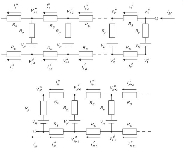
FIG. 14 (a,b) MOSFET with parallel current flow

Again, Krieger proposed that we establish an incremental model, where each contact defines an electrical node, and each region between each contact to be modeled as a resistor element [43]. Krieger defined a network, where the lateral resistance between each physical contact can be defined as a resistor Rs. The MOSFET is represented as a voltage source VH (whose magnitude is the holding voltage) and a local term Rp, which represents the dynamic on resistance Rd divided by the number of electrical nodes along the electrical network. In this fashion, the MOSFET structure is re-represented as a resistive ladder network with a voltage source between the upper and lower segment of the ladder network.
To solve for the solution of the voltage distribution in the MOSFET structure, the boundary conditions must be established. In the case of the parallel current flow, establishing a boundary condition, that the current flows out the bottom of the left-hand side (LHS), and the electrical connections on the right-hand side (RHS) is the source of incoming current. For current conservation, the incoming current in the drain is equal to the outgoing source current.
In the network, it is assumed that the wire resistance of the MOSFET drain and that of the source are equal in magnitude, and the contact density is the same. In this fashion, the MOSFET can be divided into equal segments on the upper and lower regions. Along the top and bottom of the network, the regions are segmented with resistors Rs. Between the upper and lower parts of the circuit network, they are electrically connected using resistor Rp and voltage source VH.
Incrementally, the voltage drop from the upper node to the lower node is equal to the voltage drops across the network at a node. The current flowing through that nodal point is the current, which is not flowing down the upper region
This can also be represented as the current not flowing between two sequential contacts on the lower segment of the structure,...
… additionally, the voltage drops along the metal line can be represented by the current flowing down the upper and lower wiring times the resistance drop
Using the above four expressions, we can solve for the respective voltage drops from the upper to lower segment as a function of the currents and resistances as well as the voltage differentials associated with the current differencesr simplicity, the following values are defined as [...]
5. ESD MOSFET DESIGN: SILICIDE MASKING
5.1 Silicide Mask Design
In the ESD design practice, resistor ballasting is introduced into MOSFET structures to prevent MOSFET second breakdown [38]. MOSFET resistor ballasting has two roles:
_ Introduction of MOSFET series resistance.
_ Introduction of MOSFET lateral resistance.
The MOSFET series resistance serves a first purpose of limiting the current in a MOSFET during ESD events. The role of the series resistance establishes a current limit through the MOSFET structure. In the case that the MOSFET has an ESD element in a parallel ESD current loop, the voltage drop incurred by the series resistance allows for the current to flow through the ESD current loop, buffering the MOSFET network, as well as establishing an increase in the voltage margin of ESD network operation prior to MOSFET failure.
A second aspect is the introduction of MOSFET lateral resistance. The introduction of MOSFET lateral resistance provides lateral ballasting. This is a second ESD design practice of utilization of the MOSFET width by improving the MOSFET ''effective width.'' Current constriction occurs during self-heating in the MOSFET source and drain regions. With the introduction of lateral ballasting, lateral current flow is minimized.
Refractory metal are deposited on MOSFET source, drain, and gate regions to lower the MOSFET series resistance for improved MOSFET functionality. The refractory metal is deposited on the silicon surface forming a silicide compound. The silicide lowers the series resistance of the MOSFET source, drain, and gate significantly enough to lower the ESD robustness of the semiconductor device. The silicide formation is self-aligned to the MOSFET physical regions, and is commonly referred to as self-aligned silicide or salicide.
A second aspect is that the low-resistance silicide film is in parallel with the MOSFET silicon diffusion. Given the resistance is significantly lower than the silicon region, the majority of the current flow is contained within the silicide film, leading to high current densities in the silicide film. A third ESD aspect is that the silicide consumes the silicon atoms and forms close to source and drain metallurgical junction; this can lead to a lowering of the MOSFET ESD robustness due to silicide penetration. During ESD events, the MOSFET drain region undergoes self-heating. The peak local temperature in the MOSFET drain region can lead to refractory metal penetration to the metallurgical junction. This will lead to physical failure and leakage. Additionally, the presence of LOCOS or STI triple points (e.g., between the silicide, the silicon junction, and isolation structure) can lead to MOSFET ESD failure.
A technique to improve the MOSFET ESD robustness is to eliminate the self-aligned nature of the silicide formation, and place it in regions that provide ESD advantages and eliminate ESD disadvantages. Silicide is an advantage under the contacts to provide good ohmic contacts between the silicide film and the silicon surface. Silicide is also important on the MOSFET gate structure in the case of MOSFET structures that have narrow channels and long MOSFET widths (e.g., MOSFET OCD driver structures). The locations where silicide is a disadvantage are the MOSFET source and drain region between the MOSFET contact and gate region, and MOSFET isolation edges.
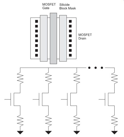
FIG. 15 (a) Example of MOSFET ESD design using silicide block mask on
MOSFET source and drain; (b) Circuit schematic of the MOSFET ESD design with
MOSFET source and drain multi-finger ballasting
5.2 Silicide Mask Design Over Source and Drain
FIG. 15 (a) shows an example of the MOSFET structure with a silicide block mask on the MOSFET source and drain regions. In this ESD design practice, the silicide is formed under the MOSFET contacts and near the MOSFET gate structure but not in the center region of the MOSFET. The advantage of this design practice is that good contact resistance is established in the MOSFET structure. The second advantage is the MOSFET polysilicon gate sheet resistance is maintained. The disadvantage of this implementation is that space is required between the silicide mask and the MOSFET gate mask; between the two regions there exists a small region of salicide in the overlay space. An issue exists in this implementation with some forms of refractory metals. In the case of titanium silicide, as the area decreases, the probability of transformation from the high-resistance phase state to the low-resistance state phase decreases. Hence, the physical area and the transformation probability introduces uncertainty in the nature of the silicide and lateral resistance near the gate structure. As the contact-to-gate increases, the series resistance will increase between the MOSFET structure.
FIG. 15 (b) shows a circuit schematic of a n-channel MOSFET with MOSFET source and drain resistance ballasting. The introduction of the salicide block mask presents a series resistor in the MOSFET drain and the MOSFET source. In a multi-finger MOSFET structure, this introduces electrical current uniformity within the MOSFET, from MOSFET finger-to-finger. The MOSFET source resistance also introduces both electrical and thermal stability.
5.3 Silicide Mask Design Over Gate
In a second design practice, the MOSFET silicide block mask is extended from the MOSFET source-to-drain contacts (FIG. 16). In CMOS technologies that do not require the MOSFET gate structure to have silicide films deposited, the silicide can be blocked. For metal gate MOSFET structures, such as MOSFETs with tungsten (W) gate films, the blocking of the silicide is possible. It is also possible to block the silicide on polysilicon MOSFET gate structures for long-channel narrow-width MOSFET structures. This method avoids the formation of the silicide in the narrow region near the MOSFET drain-to-gate overlap region, and will be less sensitive to alignment and overlay issues.
An additional ESD design practice is to eliminate the silicide along the edges of the MOSFET source and drain isolation edges. This lowers the possibility of isolation silicide-metallurgical junction triple points that lead to ESD failure. The avoidance of the self-alignment between the MOSFET isolation edges and the silicide region has the disadvantage of additional alignment issues (e.g., silicide block mask-to-isolation spacing).
The advantage of this ESD design practice is the lack of sensitivity to the semiconductor drain junction and isolation design.
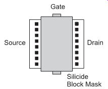
FIG. 16 MOSFET ESD design practice with silicide blocking from MOSFET
source-to-drain contacts.
A fourth ESD design practice is separation of the silicide between the contacts. In the silicided contact region, the silicide between the drain contacts in the drain contact-to contact space can be removed to introduce more lateral ballasting at the drain region.
The advantage of this technique is the introduction of the ballasting in the contact region.
The disadvantage of this technique is twofold. First, the model prediction of the resistance is more difficult. Second, the overlay between the contact and the silicide block masks impacts the contact-to-contact space and contact density. In one implementation, each contact had its own interconnect wire. The MOSFET OCD was connected with a set of parallel wires and parallel contacts. Where this would seem that this would provide the best ESD ballasting, in actuality, the ESD failure mechanisms occurred at the contacted areas due to high current densities in some of the physical contacts.
5.4 Silicide and Segmentation
MOSFET resistor ballasting can also be introduced by creation of spaces in the MOSFET source and drain area laterally along a single MOSFET gate. This concept was first implemented in microprocessors in the early 1990s using n-well resistors and MOSFETs.
FIG. 17 shows an example of resistor ballasting within a single MOSFET finger. In this concept, the MOSFET source and drain is segmented along the MOSFET polysilicon gate finger. Using a single-finger MOSFET, the MOSFET source and drain are ''cut'' with a minimum space between the drain and source segmentations. The introduction of the segmentation prevents lateral current constriction along the length of the MOSFET structure.
The advantage of this ESD design method is that only a small segment of the MOSFET channel width is sacrificed along the MOSFET length, without the need for a salicide blocking mask. The decrease in the MOSFET channel width can be recovered by lengthening of the MOSFET finger and maintaining the total MOSFET design channel width. In the early implementations of this concept, an n-well resistor was also integrated with each segmentation. The contacts of the MOSFET were placed at the end of the n-well resistor element. Each n-well element was integrated with the MOSFET segment along the MOSFET channel width.
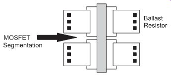
FIG. 17 MOSFET ESD design of resistor ballasting within a single MOSFET
polysilicon gate.
In a multi-finger implementation, these segmented MOSFET fingers were then placed in parallel, forming a multi-finger MOSFET with both intra- and inter-finger resistor ballasting.
In the MOSFET layout design, the resistor ballasting can be established in (a) the MOSFET drain only, (b) the MOSFET source only, and (c) the MOSFET source and drain.
Additionally, in the multi-finger implementation, the MOSFET fingers can be ''mirrored'' sharing contacts at the MOSFET source or drain region. In the design, for density reasons, only MOSFET drain resistor ballasting is introduced. Additionally, for improving the MOSFET finger-to-finger snapback uniformity, local p+ substrate contacts can be placed between each the MOSFET fingers at the MOSFET source. The options in this ESD design practice are as follows:
_ Intra-finger MOSFET resistor ballasting of the MOSFET drain only.
_ Intra-finger MOSFET resistor ballasting of the MOSFET drain and source.
_ Multi-finger MOSFET with both intra- and inter-finger resistor ballasting.
_ Introduction of local substrate contacts between the MOSFET multi-finger MOSFET.
Another ESD design methodology can establish segmentation without the utilization of the local resistor elements (first introduced by S. Voldman and D. Hui). Instead of introducing local resistor elements within the single MOSFET finger, the segmentation along a single finger can be introduced without the local resistor. The disadvantage of the local resistor elements and salicide block masks is the extra loading capacitance and area impact. Segmentation and lateral ballasting can be introduced by ''cutting'' across a full multi-finger MOSFET whose dimensions are all minimum spacing (e.g., minimum contact to-gate, contact-to-contact, gate-to-gate, etc.). No substrate contacts are introduced between the MOSFET fingers to reduce area impacts. The ''cut'' is introduced perpendicular to the MOSFET polysilicon gate structure; this introduces a lateral MOSFET resistor ballasting. In series with the multi-finger structure is a series resistor element for each cut segmentation.
This ESD design method introduces intra-finger resistor ballasting, and introduces a global single resistor with each segmentation (for all MOSFET fingers) instead of a separate series resistor for each MOSFET finger. From a MOSFET layout area, and loading capacitance issue, this ESD design method is significantly more efficient than the individual resistor for each multi-finger element. This method introduces effectively intra-finger MOSFET ballasting, and avoids the multi-finger ballasting across the MOSFET fingers. With the smaller area, the distance from the local p+ substrate contact is comparable MOSFET finger-to-finger. The ESD design methodology is as follows:
_ Design multi-finger MOSFET to minimum design rules (e.g. gate pitch, contact-to-gate, contact-to-contact)
_ Place resistor element along the channel width
_ Introduce source and drain ''cut'' segmentations perpendicular to the MOSFET polysilicon
fingers using isolation structure with the ''cut'' width is the minimum isolation width.
_ Introduce the same ''cut'' line through the resistor element, segmenting the single resistor into a multiple resistor element.
6. ESD MOSFET DESIGN: SERIES CASCODE CONFIGURATIONS
6.1 Series Cascode MOSFET
For mixed voltage interface (MVI), MOSFET devices are placed in a series cascode configuration to minimize the MOSFET drain-to-gate voltage. Reduction of the MOSFET drain-to-gate voltage avoids hot electron voltage degradation, as well as reduces the MOSFET gate oxide stress. FIG. 18 shows an electrical schematic of a multi-finger series cascode MOSFET element. The example circuit schematic shows the introduction of a MOSFET drain resistor element in series with each MOSFET finger as a ballasting element. In these implementations, the operation of the series cascode MOSFET network in ESD environments is a function of the physical layout implementation of this circuit schematic.
There are two circuit design practices for forming a series cascode MOSFET:
_ Series cascode MOSFETs are spatially separated with different source and drain diffusions, and interconnected using metal levels.
_ Series cascode MOSFETs are spatially integrated using a common isolation region, with the source and drain diffusions are defined by the array of MOSFET polysilicon gate structure.
In the case of the spatially separated series cascode MOSFET, the design practice is similar to a single multi-finger MOSFET. When placement of the two elements is in series, the series cascode MOSFET snapback will be the sum of the MOSFET snapback voltages. In this fashion, no current will flow through the MOSFET structures until the series cascode MOSFET snapback voltage is achieved. The advantage of this implementation (for a MOSFET OCD that requires ESD protection) is that the placement of the second MOSFET element provides more voltage margin in the network prior to current conduction. This allows the ESD current to flow through an alternate ESD current loop. The disadvantage is that more area is required for the physical contacts and wiring interconnects.
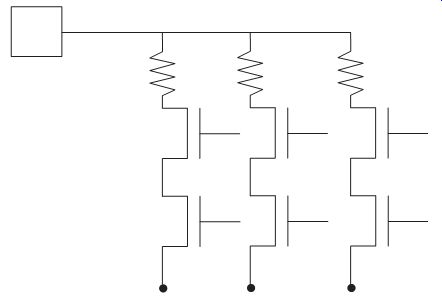
FIG. 18 Multi-finger series cascode MOSFET structure (with drain resistor
ballasting)
6.2 Integrated Cascode MOSFETs
By integration of the first- and second-series MOSFETs, the two transistors are spatially integrated into a single isolation opening. With the integrated series cascode MOSFETs, the MOSFET source of the first transistor is also the same physical diffusion as the MOSFET drain of the second transistor (see FIG. 18). The two MOSFET gates are placed with no physical contacts between the regions; in this fashion, the first MOSFET source contacts and second MOSFET drain contacts are eliminated, as well as the associated interconnects. This design layout style provides a higher utilization of silicon area for the MOSFET network.
Without the presence of the first MOSFET source contacts and the second MOSFET drain contacts, the spacing between the first and second MOSFET gate structures can be minimum. With the integration, a new ESD MOSFET design parameter of interest is the MOSFET gate-to-gate spacing. In this method of integration, the MOSFET gate-to-gate spacing can be reduced well below the MOSFET gate-to-contact spacing.
In the case of a multi-finger MOSFET structure, a non-uniform gate-to-gate spacing occurs if the gate-to-contact space does not match the gate-to-gate spacing. From the discussion of MOSFET linewidth control, the non-uniform spacing of gate pitch can lead to nested-to-isolated linewidth offset. This can lead to MOSFET finger-to-finger channel length variations, which can lead to systematic non-uniform MOSFET second breakdown.
In the integrated series cascode MOSFET structure for MOSFET OCD networks as a MOSFET pull-down network, the MOSFET drain of the first transistor is connected to the input node and the MOSFET source of the second transistor is connected to the ground rail (e.g., VSS) or chip substrate. MOSFET snapback is initiated by a high voltage being applied to the MOSFET n-channel drain. At the MOSFET drain-to-gate region, avalanche breakdown-generated electron-hole pairs are formed in the depletion region. As the substrate current increases, the local substrate potential decreases, leading to forward biasing of the MOSFET source of the second transistor. In this series cascode structure, since the first transistor MOSFET source is floating, it cannot sustain the MOSFET snapback current. For the series cascode MOSFET structure, the localness of the first and second transistor leads to the forward biasing of the MOSFET source of the second transistor. In parallel with the series cascode MOSFET structure, a parasitic bipolar transistor is formed between the MOSFET drain of the first transistor, the substrate, and the MOSFET source of the second transistor. This parasitic element is then a function of the spacing between the MOSFET drain of the first transistor and the MOSFET source of the second. The effective MOSFET bipolar transistor width is the sum of the first MOSFET gate length, the MOSFET gate-to gate spacing, and the second MOSFET gate length.
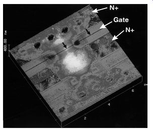
FIG. 19 Atomic force microscope (AFM) image of the series cascode MOSFET
structure
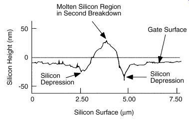
FIG. 20 Silicon height in the series cascode MOSFET gate structure in
the first MOSFET gate through the MOSFET current constriction region
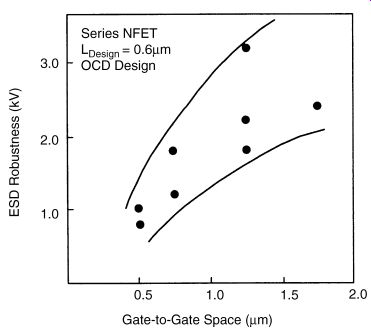
FIG. 21 HBM ESD robustness of an application as a function of the series
cascode MOSFET gate-to-gate spacing.
The first evidence of the interaction of the two MOSFETs was evident from scanning electron microscope (SEM), transmission electron microscope (TEM), and atomic force microscope (AFM) imaging by Never and Voldman. FIG. 19 shows the AFM image of a multi-finger series cascode MOSFET structure after MOSFET second breakdown occurs. The first point of interest is that the failure analysis shows that the MOSFET failure between the first and second transistor is a local phenomenon between a group of first MOSFET drain contacts and a second group of second MOSFET source contacts. MOSFET current constriction is evident in the MOSFET gate region. This is followed by a widening in the MOSFET gate-to-gate region where titanium silicide is present. The low resistance silicide region allowed for the widening of the MOSFET current constriction. As the current flow continues under the second MOSFET gate, the current constriction occurs which broadens as it extends to the second MOSFET source contacts. FIG. 20 shows the silicon surface of the series cascode structure after MOSFET second breakdown. A cross-section was taken parallel to the current flow through the MOSFET second breakdown constriction region, under the first MOSFET gate region. In the center of the MOSFET second breakdown, molten silicon of height 20 nm is present with silicon depressions on both sides. The height of the molten silicon is above the MOSFET gate surface.
The first ESD measurements on the series cascoded MOSFET structure were demonstrated in a STI-defined 0.25-mm channel length technology by Voldman. FIG. 21 shows that the HBM ESD robustness of a series cascode MOSFET multi-finger structure increases with increased MOSFET gate-to-gate spacings. MOSFET device ESD HBM robustness increased from to 2.5 kVas the MOSFET gate-to-gate space increased from 0.5 to 1.5 mm.
As an example implementation, the MOSFET gate-to-gate spacing was varied in a design with a fixed-size ESD network, and fixed OCD pull-up design. In the series-cascode design, the series cascode MOSFET structure in a design implementation, the ESD design remained fixed, but the gate-to-gate spacing was increased from 0.5 to 1.5 mm. Experimental results showed increasing HBM ESD robustness from 4 to 6 kV with the increased spacing.
7. ESD MOSFET DESIGN: MULTI-FINGER DESIGN INTEGRATION OF COUPLING AND BALLASTING TECHNIQUES
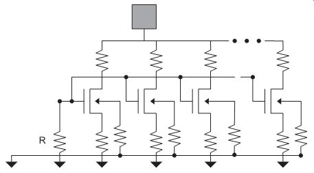
FIG. 22 Grounded-gate resistor-ballasted MOSFET with gate resistor element
A fundamental ESD concept is that to provide good current uniformity in a multi-finger MOSFET structure, it is understood that given the MOSFET second breakdown voltage, Vt2 , exceeds the MOSFET first breakdown voltage, Vt1. In a standard semiconductor process, the typical condition is the opposite, which leads to a non-uniformity of current distribution in a multi-finger MOSFET. But, using ballasting, coupling, and biasing techniques, the MOSFET second breakdown voltage, Vt2 , can exceed the MOSFET first breakdown voltage, Vt1 , leading to MOSFET current uniformity in a multi-finger MOSFET structure. Multi-finger MOSFET ESD design utilizes both coupling, and ballasting concepts to improve the current uniformity during high-current events. Coupling and ballasting techniques can be integrated together to provide improved ESD robustness. The following implementations utilize both gate coupling and resistor ballasting:
_ Substrate grounded-gate (with gate resistor) resistor-ballasted multi-finger MOSFET.
_ Substrate grounded-gate (with gate resistor and capacitor element) resistor-ballasted multi-finger MOSFET.
_ Soft substrate grounded-gate resistor-ballasted multi-finger MOSFET.
_ Domino source-to-gate coupled resistor-ballasted multi-finger MOSFET.
_ MOSFET source-initiated gate-bootstrapped resistor-ballasted multi-finger MOSFET with MOSFET.
_ MOSFET source-initiated gate-bootstrapped resistor-ballasted multi-finger MOSFET with diode.
7.1 Grounded-Gate Resistor-Ballasted MOSFET
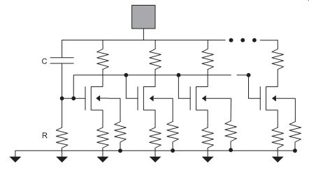
FIG. 23 Grounded-gate resistor-ballasted MOSFET with gate resistor element
and external capacitor element
FIG. 22 shows a substrate grounded-gate resistor-ballasted multi-finger with a resistor between the MOSFET gate and the substrate ground. In this configuration, the gate structure is connected to the ground potential through a resistor element [48]. The resistor element introduces a ''soft-ground'' and allows for RC-coupling of the physical element associated with the resistor, the MOSFET drain-to-gate capacitance (e.g., overlap capacitance). In this implementation, as the potential on the signal pad increases, the MOSFET gate is coupled, leading to a rise in the MOSFET gate potential. The MOSFET gate resistor allows for the MOSFET gate voltage to couple with the input node signal. As the MOSFET gate rises to the MOSFET threshold voltage, MOSFET current conduction is initiated. As the current flows into a given MOSFET finger, the voltage across the drain resistor element leads to a de biasing effect. This limits the voltage drop across the given element, allowing for the current to distribute to adjacent MOSFET fingers.
In a small modification of the substrate grounded-gate (with gate resistor) resistor ballasted multi-finger MOSFET, a capacitor element can be placed externally in parallel with the MOSFET gate-to-drain capacitance (FIG. 23). Maloney highlighted that an additional capacitor element can be placed in a parallel fashion between the MOSFET drain and the MOSFET gate electrode. As the capacitor size increases, the MOSFET gate capacitive couples to the MOSFET drain during a positive ESD event on a pad. As the MOSFET gate voltage increases, MOSFET conduction is initiated, leading to improved current uniformity.
7.2 Soft Substrate Grounded-Gate Resistor-Ballasted MOSFET
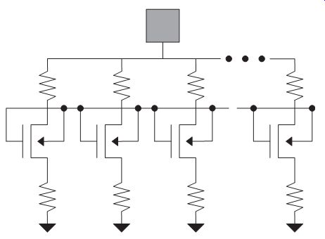
FIG. 24 Soft grounded-gate resistor-ballasted multi-finger MOSFET
''Soft'' substrate grounded-gate resistor-ballasted multi-finger MOSFET (e.g., s-ggNMOS) allows the electrical connection of the MOSFET gate structure to increase in potential relative to the semiconductor chip substrate. As in the prior developments, the MOSFET gate potential is allowed to increase. As the MOSFET gate increases to the MOSFET threshold voltage, the MOSFET will conduct current from the MOSFET drain to the MOSFET source, allowing current to flow from the signal pad to the semiconductor chip substrate.
FIG. 24 is a representation of a ''soft'' grounded-gate resistor-ballasted multi-finger MOSFET (ss-ggNMOS) as represented by Mergens et al. A resistor element is placed in series with the MOSFET drain and the source element for each individual MOSFET finger to introduce MOSFET source and drain resistor ballasting. The MOSFET gate structures are electrically connected across all the MOSFET fingers to allow the MOSFET gate potential coupling between the fingers. In this gate-biasing technique, a local substrate contact is placed near the MOSFET source and drain, but electrically decoupled from the metal VSS power bus. Two key points in this implementation are that the MOSFET drain and source are electrically coupled to the signal pad and the VSS power rail, and the MOSFET gate electrode is resistively decoupled from the VSS power rail, and responds to local substrate perturbations from injection phenomenon in the region of the MOSFET source and drain. As the MOSFET drain potential increases, electrons are attracted to the MOSFET drain region in the metallurgical junction. As the potential increases, electron-hole avalanche occurs. The hole generation flows in the metallurgical junction to the substrate region. The hole injection local to the MOSFET drain increases the local potential, leading to MOSFET snapback of the first MOSFET finger; this is followed by other MOSFET fingers undergoing MOSFET snapback. As the local potential increases, the MOSFET local substrate contact increases, leading to the MOSFET gate to increase in potential. Additionally, as the MOSFET local potential rises, the potential in the MOSFET channel region rises. From the MOSFET reverse body effect, the MOFET threshold voltage decreases as the MOSFET channel potential increases. When the MOSFET gate electrode increases to the MOSFET threshold voltage, the MOSFET source-to-drain conduction occurs. Note that in this implementation, any of the substrate contacts local to any of the MOSFET fingers introduces a MOSFET finger-to-finger coupling through the MOSFET gate structure. Also note that the MOSFET resistor ballasting acts as a ''current limit'' through any one finger between the separate MOSFET source and drain fingers. In this way, the current redistributes through the MOSFET drain structures. Additionally, the MOSFET source resistances serve to increase the electrical and thermal stability of the network.
MOSFET gate-coupling can be introduced from the MOSFET drain through overlap capacitance, additional capacitors, or through the input signal pads. MOSFET gate-coupling can also be introduced through the MOSFET source region. To initiate MOSFET source coupling, the MOSFET source potential must be allowed to increase in electric potential. A method to enable the MOSFET source potential to increase relative to the substrate potential is by resistive decoupling. This is achieved by placement of a resistor element between the MOSFET source and the VSS power rail. Introduction of a ballast resistor between the MOSFET source and the VSS power rail allows for the MOSFET source potential to increase.
7.3 Gate-Coupled Domino Resistor-Ballasted MOSFET
Mergens et al. introduced a ''domino'' method in a multi-finger MOSFET structure by electrically connecting the MOSFET gate of a second MOSFET finger to the MOSFET source of a first MOSFET finger (FIG. 25). In this domino source-to-gate coupled resistor-ballasted multi-finger MOSFET, the MOSFET source ballast resistor is split into a first and second resistor element. An electrical connection is established between the two resistor elements and electrically connected to the MOSFET gate of a second finger. This is initiated ad infinitum to all the finger elements. The ''nth finger'' MOSFET source connection is electrically connected to the MOSFET gate of the first MOSFET finger. In this fashion, the domino triggering initiation can occur in any MOSFET finger in the structure. As the signal pad increases, the electrical potential of all the MOSFET drain structure increases. As the MOSFET drain potential increases, avalanche multiplication occurs. Eventually, one of the MOSFET fingers undergoes MOSFET snapback. As the electrical conduction occurs in the MOSFET finger, the current flows through the MOSFET source resistor elements. The two resistor elements form a voltage resistor divider. As the voltage increases, the MOSFET gate structure potential increases. As the MOSFET gate potential increases, adjacent MOSFET finger begins to conduct MOSFET source-to-drain current through the MOSFET channel region. As the second MOSFET finger conducts current through its own source, the electrical potential of the MOSFET gate of the third MOSFET finger increases. This continues in this fashion, until the ''nth'' MOSFET finger. As the ''nth'' MOSFET finger undergoes MOSFET conduction, the MOSFET gate of the first MOSFET finger that underwent MOSFET snapback, will have its MOSFET gate potential increase, leading to MOSFET channel conduction instead of a MOSFET snapback state.
In this implementation, it was pointed out that the nature of the conduction and response in the ''Domino'' multi-finger MOSFET is different from other multi-finger MOSFETs, in the following ways:
_ The response of the network is current-driven (as opposed to frequency-driven).
_ The response is a ''static'' phenomenon not ''dynamic.''
_ The time response of the network is associated with the MOSFET gate delay time and the number of MOSFET finger stages.
The operation time is ''auto-timed'' and acts only during a fixed time interval associated with the RC response of the successive stages, the MOSFET gate delay, and the number of successive stages.
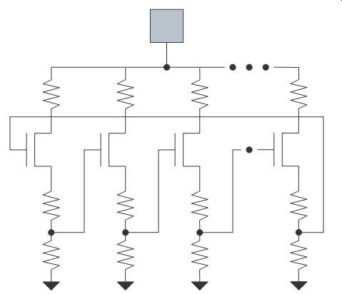
FIG. 25 Domino source-to-gate coupled resistor-ballasted multi-finger
MOSFET
These distinctions lead to many advantages over other implementations. For example, the frequency-driven MOSFET networks are a strong function of the MOSFET overlap capacitance of the MOSFET technology, making the ESD operation a strong function of the process technology. Additionally, soft grounded-gate NMOS networks are very dependent on the substrate and p-well doping concentration as well as the design layout of the substrate contact structure and the modeling/prediction of the substrate resistance. In this implementation, the MOSFET current and the models are predictive models, as well as the circuit response.
Additional advantage of this implementation is that the turn-on of the individual stages does not require the charging of the entire MOSFET gate structure for all MOSFET fingers. In the case where all MOSFET fingers are electrically connected together, the circuit response time will be a function of the total gate electrode capacitance (i.e., number of fingers). In this case, the MOSFET finger-to-finger time response will be significantly faster due to the smaller capacitance load of the individual MOSFET finger.
7.4 MOSFET Source-initiated Gate-Bootstrapped Resistor Ballasted Multi-Finger MOSFET
With MOSFET MOS-FET source-initiated gate coupling can be initiated to individual MOSFET fingers sequentially or all MOSFET fingers simultaneously. In an domino-style implementation, the MOSFET fingers are gate-coupled in a sequential manner (FIG. 26). In the soft grounded-gate MOSFET, all fingers are initiated simultaneously. In the case of the individual sequential coupling technique, the response of the individual gate structures will have a faster RC-time response for each individual fingers. But the disadvantage is the electrical disconnection of the MOSFET gate structure for utilization as a MOSFET off-chip pull down.
MOSFET source-initiated gate coupling can be implemented in a fashion, where one MOSFET source initiates a common MOSFET gate electrode. As in the domino-style implementation, a MOSFET source is electrically connected to two series resistor elements.
The center node of the two resistor elements is electrically connected to initiate MOSFET gate-coupling. With a common gate electrode, the MOSFET source connection cannot be electrically connected to the MOSFET gate. Hence, an additional bootstrap MOSFET is placed between the signal pad and the MOSFET gate electrode. The bootstrap MOSFET drain is connected to the signal pad, its source connected to the primary MOSFET gate electrode. The MOSFET source resistor center-tap is electrically connected to the gate of the bootstrap MOSFET.
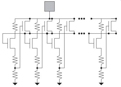
FIG. 26 MOSFET source-initiated gate-bootstrapped resistor-ballasted
multi-finger MOSFET with MOSFET
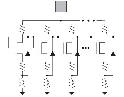
FIG. 27 MOSFET source-initiated gate-bootstrapped resistor-ballasted
multi-finger MOSFET with diode bootstrap element
In this network, the first conducting MOSFET finger source senses the ESD event, leading to a rise in the MOSFET source potential. This first MOSFET finger source rises. The electrical potential of the MOSFET source resistor divider leads to an increase in the gate of the corresponding bootstrap MOSFET element. The bootstrap MOSFET undergoes MOS-FET conduction when the MOSFET threshold voltage is exceeded. The bootstrap MOSFET element charges up the MOSFET gate electrode, leading to MOSFET conduction in the other adjacent MOSFET fingers, which were not undergoing MOSFET snapback. The advantage of this method allows for electrical connection of the primary MOSFET gate to a pre-driver network for utilization in OCD networks or other circuits. The disadvantage of this structure is the need for an additional resistor and MOSFET for every segmentation of finger elements. This adds extra capacitance loading and space impact.
7.5 MOSFET Source-Initiated Gate-Bootstrapped Resistor Ballasted Multi-Finger MOSFET With Diode
MOSFET source-initiated gate coupling can be implemented in a fashion, where one MOSFET source initiates a common MOSFET gate electrode. Utilizing a MOSFET source with two series resistor ballast elements and a center tap, MOSFET gate coupling can be initiated through a diode element. In the case that a MOSFET bootstrap element is used, this bootstrap element requires additional space as well as impacting capacitance loading on the signal pad (FIG. 27). With the utilization of a diode element between the MOSFET source and the MOSFET gate electrode, no additional loading capacitance occurs on the signal pad, and less area can be utilized. In this network, the first conducting MOSFET finger source senses the ESD event, leading to a rise in the MOSFET source potential. This first MOSFET finger source rises. The electrical potential of the MOSFET source resistor divider leads to an increase in the anode of the bootstrap p-n diode element. The bootstrap p-n diode element charges the MOSFET gate electrode when the p-n diode element becomes forward active. When the MOSFET gate electrode rises, MOSFET channel conduction occurs in all MOSFET finger elements providing uniform current flow. The advantage of this method allows for electrical connection of the MOSFET gate to a pre-driver network for utilization in OCD networks or other circuits. This method also prevents the additional loading on the signal node compared to other bootstrap methods. A disadvantage of this method is that the diode elements must charge the complete MOSFET gate electrode. As a result, this method may be limited by the diode current drive and the number of MOSFET fingers that can be driven by the bootstrap element.
8. ESD MOSFET DESIGN: ENCLOSED DRAIN DESIGN PRACTICE
Alternate ESD design practices exist that attempt to avoid metal bus distribution effects and isolation technology issues. One design practice is to create an ''enclosed'' MOSFET drain.
FIG. 28 is an example of the enclosed drain MOSFET design style. The MOSFET source encloses the area of the MOSFET structure, with a substrate contact outside of the MOSFET source. The MOSFET polysilicon gate structure is formed in a ring-like structure around the MOSFET drain; the MOSFET drain is contained within the MOSFET polysilicon gate region. In this design style, since a metal contact cannot be placed on the MOSFET polysilicon gate structure dielectric, a small isolation region is formed to ''break'' the MOSFET dielectric area. A small rectangle is formed where the polysilicon film extends over the isolation structure. At this location, a metal contact can be placed to electrically connect the MOSFET polysilicon gate structure. The metal design pattern will allow a ''broad-side'' metal connection along the full width of the MOSFET drain without metal distribution and resistance issues. For a multi-finger implementation, the design is ''mirrored'' around the MOSFET source, and multiple polysilicon rings are formed. In this implementations, there are many potential advantages. First, as discussed, the voltage distribution are minimized because of the ''broadside wiring'' that allows for no lateral distribution issue. Second, there is no isolation-dependent leakage mechanisms, junction/ salicide edge, junction/isolation edge, and triple-point junction/salicide/isolation edge issues (except at the small isolation island area for MOSFET gate connection). This design style effectively contains a polysilicon-bound MOSFET drain region, minimizing LOCOS bird's beak issues and STI pull-down. Additionally, the substrate contact is effectively equal distance from the source and drain on all sides.
In summary, the MOSFET ''enclosed drain'' ESD design practice avoids the following MOSFET issues:
_ MOSFET voltage distribution drops in metal design.
_ Technology-dependent LOCOS or STI issues.
_ Technology-dependent silicide distribution issues.
_ Equal source-to-substrate contact spacing.
9. ESD MOSFET INTERCONNECT BALLASTING DESIGN
In MOSFET ESD design, resistor ballasting can be introduced using interconnect structures.
In the ESD design practice, resistor ballasting is introduced into MOSFET structures to prevent MOSFET second breakdown. The MOSFET series resistance serves a first purpose of limiting the current in a MOSFET during ESD events. The role of the series resistance establishes a current limit through the MOSFET structure. In the case that the MOSFET has an ESD element in a parallel ESD current loop, the voltage drop incurred by the series resistance allows the current to flow through the ESD current loop, buffering the MOSFET network, as well as establishing an increase in the voltage margin of ESD network operation prior to MOSFET failure.
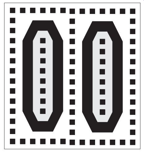
FIG. 28 Enclosed drain MOSFET ESD design
MOSFET interconnect resistor ballasting provides series resistance ballasting when connected at the MOSFET drain, and can introduce lateral ballasting by connecting to individual drain contacts. Refractory metals also exist as liner material aluminum and copper interconnect systems. Hence, resistors formed from titanium and tantalum films can serve as good ballasting elements . Refractory metal resistor films have many advantages for resistor ballasting. Using the liner materials, resistor elements have low capacitance, low skin effect, high linearity, a high melting temperature, high critical current to failure, and do not require space on the silicon surface. The resistor structure can be formed on the walls of a dielectric trough. The structure can be applied to circuit applications such as an ESD network, an RC-coupled MOSFET, a resistor-ballasted MOSFET, and others. The resistors can be in series with the MOSFET or other structures. These structures are also compatible with fuse elements.
In some technologies, there exist refractory metal ''local interconnects.'' Refractory metal layers, such as ''M0'' tungsten, can serve as resistor ballasting layers and resistor structures for ESD protection [50]. Refractory metals have the advantage of high melting temperatures.
For example, tungsten metallurgy used in ''local interconnects'' has a 3400 C melting temperature, which is significantly above silicon and dielectric melting temperatures. One advantage of the refractory metal local interconnect is that the film thickness allows to carry significant current. Utilization of a refractory metal resistor as a resistor buffering element was demonstrated by K. Duncan in a DRAM application (FIG. 29). K. Duncan and C. Brennan noted the resistance response at temperature, R(T), due to self-heating of tungsten interconnects, also provides ESD advantage.
But, it is a disadvantage of using aluminum and copper interconnects as MOSFET ballasting elements because of the low melting temperature, and low interconnect resistances of aluminum and copper. Another disadvantage is that the nature of the films change material state and crystalline structure when undergoing self-heating. A fourth disadvantage is to provide adequate resistance; the interconnect will introduce space and inductance concerns.
Removal of copper materials will allow utilization of the refractory liner for resistor ballasting elements for ESD applications.
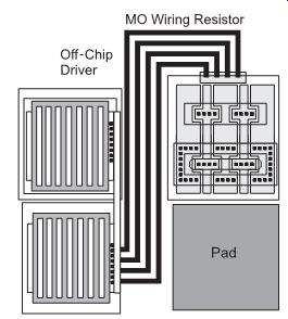
FIG. 29 M0 local interconnect in ESD MOSFET design
A design practice advantage of using interconnect ballasting over MOSFET source and drain salicide block masks is the capacitance loading and area reduction of the MOSFET structure. Prior to the ESD design practice of silicide blocking, many technologies constructed ESD designs with silicide. Silicide block masks added additional costs and space. A second advantage is the lack of parasitic mechanisms and lack of interaction with the substrate region. During CDM testing, silicon resistors are interactive and play a role in the CDM response. Hence, using interconnect ballasting elements, utilizing refractory metal resistors instead of silicon-based resistors, can have advantages as long as low-temperature materials, such as aluminum and copper, are avoided.
10. ESD MOSFET DESIGN: SOURCE AND DRAIN SEGMENTATION
Source and drain segmentation has been introduced in the early 1990s in microprocessor designs and ASIC implementation with the introduction of resistor ballasting. This was typically achieved by introducing cuts through the single- or multi-finger MOSFET structure. In this process, the MOSFET drain regions maintained a rectangular shape in the segmentation. In new concepts proposed by E. Worley, non-rectangular shapes of the MOSFET source and drain region are introduced to provide local resistance increases. For MOSFETs, E. Worley demonstrated a method of segmentation of the MOSFET source and drain region to introduce resistor ballasting and avoid area loss. The objectives of the MOSFET resistor ballasting include the following:
_ Low global parasitic series resistance relative to the MOSFET channel resistance.
_ High series resistance in series with a localized hot spot.
_ Low drain capacitance.
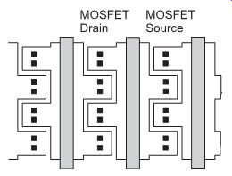
FIG. 30 Staggered ballasted MOSFET design
Worley points out that an additional ballasting objective is associated with the substrate resistance. The key factors that initiate MOSFET snapback spatial dependence are the following:
_ Proximity of substrate contact to MOSFET fingers.
_ MOSFET channel-to-substrate contact resistance.
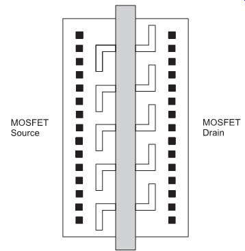
FIG. 31 Staggered segmented ballasted MOSFET design
Using a first layout scheme, Worley introduced a ''staggered'' ballasting implementation (FIG. 30). Using a second new layout scheme, known as the Staggered Segmented diffusion layout, the MOSFET source and drain layout is segmented into sections by extending the MOSFET source and drain to individual contacts between the multi-finger gate regions; this solution introduces local resistors associated with each contact. At the same time, the area on the edges is eliminated lowering the total MOSFET source/drain capacitance. Worley integrated this concept with a second layout, which allows for the local resistor and segmentation of the MOSFET along the length of the MOSFET polysilicon finger. The ''breaking'' of the MOSFET source drain at the edge of the MOSFET, as discussed in prior sections, introduces segmentation of the MOSFET along a given MOSFET finger; this can be integrated with the concept of Worley to provide another means of providing resistor ballasting. A new feature is the path at which the current must flow in order to reach the MOSFET channel region, allowing for resistor structures in parallel to the MOSFET gate width, followed by a transition perpendicular to the MOSFET channel gate width.
11. SUMMARY AND CLOSING COMMENTS
In this Section, ESD design practices and analysis are highlighted using the MOSFET as the vehicle for discussion. The ESD design practices discuss all aspects of the layout and design from the physical dimensions, the placement of the contacts, the orientation of the wiring, the placement of silicide, and isolation issues, as well as the single-versus multi-finger structure. The Section uses the solution of the cylinder and plane surface for evaluation of the microscopic heating between the contact and gate edge. The Section draws the connection of the local contact-to-gate analysis and the ladder network models of DeChairo and Krieger. In the analysis both contain resistance ratios that can be utilized as ESD design metrics. The Section then discusses the series-cascode analysis of N. Dickson, G. Gerosa, S. Voldman, and J. Never. To close the Section, we provide some of the examples, discussed by M. Mergens, that highlight multi-finger interactions, ballasting, and gate-coupling concepts.
In Section 4, the design and layout of ESD diode elements are discussed. Section 4 will discuss the ESD issues with diode elements from the wells to the interconnect layout. The Section will discuss single diode elements as well as series diodes (e.g., also referred to as diode-string diode designs) in single-, dual-, and triple-well technologies.
PROBLEMS
1. From the analysis of the electric field and current from a contact of radius, R, shows that the denominator can be put in the form of an inverse hyperbolic cosine (e.g., cosh_1 (x)) form. What is the characteristic ratio of the solution? Show an equivalency to the logarithm expression.
2. Derive the equation for the locus of points that form equi-energy surfaces in the two dimensional plane. Solve the fourth order quadratic equation.
3. Derive the current density at the MOSFET gate (e.g., x = 0) case for a single contact. Derive the lateral current density.
4. Assuming that the temperature field from a single contact is proportional to the square root of the product of the current density and electric field. Derive the temperature field.
5. Assume the heat fluence is equal to minus the derivative of temperature, solve for the heat flux laterally along the MOSFET device from the single contact. Derive the heat flux in the x- and y-dimension.
6. Solve the current density for a set of N contacts, which are spaced at a center-to-center spacing of value b, assuming superposition of the N contacts. Solve for the peak current density.
7. Given N contacts, and allowing for superposition of the current equation, what spacing b achieves the most uniform current density at the MOSFET gate (e.g., x = 0 plane)?
8. Show the relationship between the solution of spreading resistance from a single contact in the electrical field solution. Derive the spreading resistance from the contact of radius R to the MOSFET gate (e.g., x = 0 plane). Relate this to a resistive ladder network.
9. Given the DeChairo ladder network model, derive the maximum voltage and current differential between the first finger and the Nth finger.
10. Given the Duvvury ladder network model of broad-side connection of a multi-finger MOSFET structure on the drain, a finger resistance RF, and a source finger-to-finger bus resistance of Rs, assume that the end resistances are double the center resistance since the last fingers are not folded (e.g., one-sided). Given N drain fingers, solve the relationship resistance matrix as a N-2 region, with two different end resistances RE.
What is the recursive relationship at the ends? Derive the resistance matrix and current in each current loop in the ladder network.
11. Given the anti-parallel current flow in a single-finger MOSFET, using the Krieger model, what is the voltage drop between the two ends of the MOSFET finger (e.g., along the upper wire)?
12. Given the parallel current flow in a single-finger MOSFET, using the Krieger model, what is the maximum voltage drop along the MOSFET finger (e.g., along the upper wire)?
13. Assume that ESD failure does not occur as the voltage is raised into MOSFET second breakdown, Vt2. Derive a relationship for the parallel and anti-parallel cases of the percentage of the wire width that is above Vt2 as a function of current source magnitude.
Prev. | Next