AMAZON multi-meters discounts AMAZON oscilloscope discounts
1. Testing for ESD, EMI, EOS, EMC, and Latchup
In the electronics industry, testing of components and systems is a part of the process of qualifying and releasing products. Standards are established to provide methodology, process, and guidance to quantify the technology issue. Testing is performed to evaluate the sensitivity and susceptibility of products to electric, magnetic, and electromagnetic events.
These can be categorized into electrostatic discharge (ESD), electrical overstress (EOS), electromagnetic interference (EMI), and electromagnetic compatibility (EMC) events, and latchup (FIG. 1). In the electronic industry, tests and procedures have been established to quantify the influence of these events on components and systems associated with ESD, EOS, EMC, and latchup.
2. Component and System Level Testing
In the testing of electronics, different tests and procedures were established that tested components, and other tests for testing of systems. These tests have been established based on the environment that the components and systems experience in processing, assembly, shipping, to product use.
FIG. 2 shows examples of component tests that are applied to wafer level, packaged and unpackaged products. Today, it is common to test semiconductor components for the following standards. These include the human body model (HBM), machine model (MM), charged device model (CDM), to transmission line pulse (TLP), and very fast transmission line pulse (VF-TLP). In the future sections, these tests are discussed in depth.
FIG. 3 shows examples of system level tests that are applied to systems to address the robustness to environments that the systems may experience in product use. For system level tests, it is now common to test for the IEC 61000-4-2, human metal model (HMM), IEC 61000-4-5, and cable discharge events (CDE).
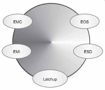
FIG. 1 ESD, EMI, EOS, and EMC
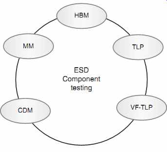
FIG. 2 Component tests
3. Qualification Testing
Many of the tests are used for different purposes. Some electrical tests are established for characterization, whereas other tests have been established for qualification of components or systems. Qualification tests are performed to guarantee or insure quality and reliability in the system, or in the field. FIG. 4 shows examples of qualification tests that are performed in the electronic industry. These qualification tests include standard practice (SP) documents, to standard test method (STM).
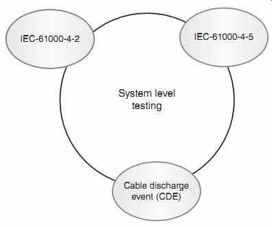
FIG. 3 System level tests
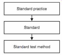
FIG. 4 Qualification testing
4. ESD Standards
In the development of these qualification processes, different types of documents and processes are established. In standards development, practices and processes are established for the quality, reliability, and release of products to customers.
4.1 Standard Development - Standard Practice (SP) and Standard Test Methods (STMs)
In the development of these qualification processes, a standard practice is established for testing of components and systems. A standard practice (SP) is a procedure or process that is established for testing. The document for the standard practice is called the standard practice (SP) document. A second practice is to establish an STM. The distinction between the standard practice (SP) and an STM is the STM procedure insures reproducibility and repeatability. In standards development, both standard practices (SP) and STM are established for the quality, reliability, and release of products to customers.
4.2 Repeatability
In STM development, repeatability is an important criterion in order to have a process elevate from a standard practice to an STM. It is important to know that if a test is performed, the experimental results are repeatable (FIG. 5).
4.3 Reproducibility
In STM development, reproducibility is a second important criterion in order to have a process elevate from a standard practice (SP) to an STM. Reproducibility is key to verify that the experimental results can be reproduced (FIG. 6).
4.4 Round Robin Testing
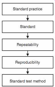
FIG. 5 Repeatability and Reproducibility
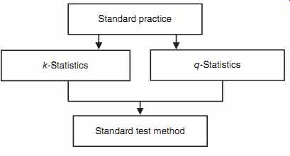
FIG. 6 SP to STM Process
In order to determine if a standard practice can be elevated to an STM, reproducibility and repeatability are evaluated in a process known as Round Robin (RR) process. Statistical analysis is initiated to determine the success or failure of reproducibility and repeatability as part of the experimental methodology. RR is an interlaboratory test that can include measurement, analysis or performing an experiment. This process can include a number of independent scientists and independent laboratories. In the case of ESD and EOS testing, different commercial test equipment is used in the process. To assess the measurement system, the statistics of analysis of variance (ANOVA) random effects model is used.
4.5 Round Robin Statistical Analysis - k-Statistics
In the RR process, the within-laboratory consistency statistics is known as the k-statistics.
The k-statistics is the quotient of the laboratory standard deviation and the mean standard deviation of all the laboratories. These can be visualized using Mandel statistics and Mandel plots. Mandel's k is an indicator of the precision compared to the pooled standard deviation across all groups. Mandel's k plot is represented by a bar graph (FIG. 7).
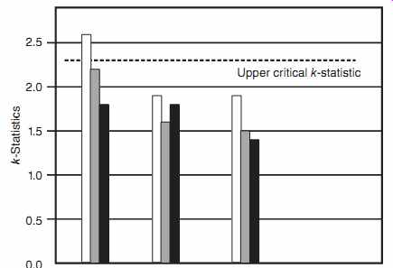
FIG. 7 Mandel k-statistics plot
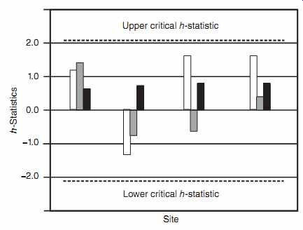
FIG. 8 Mandel h-statistics plot
4.6 Round Robin Statistical Analysis -- h-Statistics
In the RR process, the between-laboratory consistency statistics is known as the h-statistics.
The h-statistics is the ratio of the difference between the laboratory mean and the mean of all the laboratories, and the standard deviation of the means from all the laboratories.
These can be visualized using Mandel statistics and Mandel plots. Mandel's statistics are traditionally plotted for interlaboratory study data, grouped by laboratory to give a graphical view of laboratory bias and precision. Mandel's h-plots are bar graphs around a zero axis (FIG. 8).
5. Component Level Standards
Today, in the semiconductor industry, components are tested to the HBM, MM, and CDM. These tests are traditionally done on packaged components. In these tests, the components are also unpowered. For the qualification of semiconductor components for over 20 years, the HBM, MM, and CDM tests were completed prior to shipping components to a customer or system developer. In addition, latchup qualification was required in the shipping of components since the 1980s time frame. A new test of components includes the HMM test to evaluate the influence of the components on system level tests.
In the 1990s, TLP testing became popular and is now a common characterization practice in the semiconductor industry. TLP testing did not have an established methodology until the year 2003. TLP testing is performed on test structures, circuits, to components. This was followed by a second test method known as the VF-TLP testing method. VF-TLP testing is also completed on test structures to components. These TLP tests can also be performed on systems.
6. System Level Standards
System level standards are to address the sensitivity and susceptibility of electronic systems in shipping, handling, and usage environment. The objective is to simulate events that can occur.
A distinction between many of the component standard tests and the system standards is the failure criteria. In system testing, the failure can be nondestructive and destructive. System level interrupts and disturbs can be regarded as a system failure.
System testing can be evaluated with all the modules of the system assembled or unassembled. System level testing can be with or without the cable connections between the system modules.
System level standards can include direct current (DC), alternating current (AC), pulse events, as well as transient phenomena. In the text, the system level tests known as IEC 61000-4-2 and IEC 61000-4-5 are discussed. In addition, CDE is discussed from charged cables.
7. Factory and Material Standards
In the semiconductor industry, there exist ESD and EOS standards for the factory and assembly environments [10]. ESD concerns in manufacturing are a combination of the materials, tooling, and the human factors. The materials influence the triboelectric charge transfer. The tooling used can lead to charge transfer, and operators can participate in this transfer process.
In the manufacturing area, the electric field between the ceiling and the floor is influenced by the height of the ceiling, air flow, and placement of the ionizers. The placement of the ionizers relative to the work surface where the sensitive parts are placed influences the effectiveness of the ionizers. The work surface material and its physical size is also a factor.
Operators in the manufacturing line can influence triboelectric charging process. All external surfaces of the operator, type of materials, and proximity of the operator to the item can influence the charge transfer, and the human-induced electric field imposed. The footwear, garments, wrist straps, and personnel grounding of the garments can all influence the impact of the operator on tribocharging and the ESD discharge. In addition, seating, position, and distance of the operator from the sensitive parts can also influence the electric fields.
The choice of ESD materials in a manufacturing environment can have a large effect on the ESD protected area (EPA). The material choice can influence its initial conductivity, as well as the conductivity as a function of time. Material coatings and cleaning processes can influence the material conductivity. The wearout of a floor or garment can influence its global conductivity as well as its spatial variation. It is these factors why it is important to qualify a manufacturing environment, establish a measurement set of procedures, and temporal audits of the items used in the manufacturing sector.
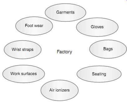
FIG. 9 Factory and material standards
The manufacturing environment consists of the following categories (FIG. 9):
• Grounding and bonding systems
• Work surfaces
• Wrist straps
• Monitors
• Footwear
• Flooring
• Personnel grounding with garments
• Ionizers
• Seating
• Mobile equipment
• Packaging.
Manufacturing test equipment is needed for evaluation of compliance to specifications. ESD test equipment includes the following:
• DC ohmmeter
• Electrodes
• Handheld electrodes
• Foot electrode
• AC outlet analyzer
• AC circuit tester (impedance meter)
• Insulative support surface
• Charged plate monitor
For all these items, it will be required to verify the electrical measurements. In order to verify compliance, electrical measurements will be the means of determining an "ESD safe" environment and compliance with objectives.
8. Characterization Testing
In component and system evaluation, characterization of the electrical characteristics is also done during the product development, assembly, and shipping.
8.1 Semiconductor Component Level Characterization
In component evaluation, characterization of the electrical characteristics is also done during the product development, assembly, and shipping. These can be performed on a component level in packaged and unpackaged form.
8.2 Semiconductor Device Level Characterization
Characterization of the electrical characteristics can be completed on a semiconductor device level. ESD testing can be performed on individual devices in a semiconductor technology to evaluate the electrical characteristics, electrical response, failure mechanisms, and ESD robustness.
8.3 Wafer Level ESD Characterization Testing
Characterization of the electrical characteristics of semiconductor devices is typically per formed on a wafer level. For wafer level ESD characterization, a probe station and adequate probes are required for ESD testing. Commercial test systems now accommodate wafer level testing. Wafer level ESD testing can be performed on individual devices in a semiconductor technology to evaluate the electrical characteristics, electrical response, failure mechanisms, and ESD robustness. Semiconductor devices can be integrated into bond pad sets to probe the components (FIG. 10).
In semiconductor development, ESD networks can also be built into bond pad sets for development of ESD networks. These can be constructed with or without electrical circuits attached.
---------
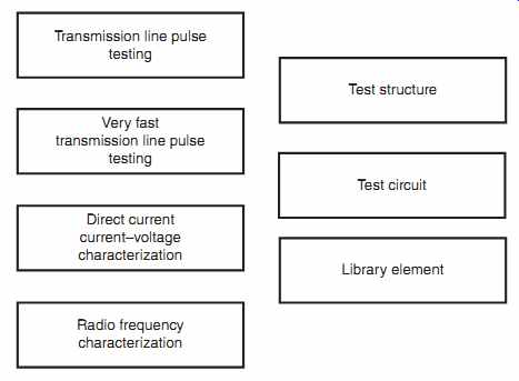
FIG. 10 Semiconductor chip level characterization
Test structure Test circuit Library element Radio frequency characterization Transmission line pulse testing Very fast transmission line pulse testing Direct current current-voltage characterization
----------
8.4 Device Characterization Tests on Circuits
Characterization of the electrical characteristics of circuits can be evaluated on a wafer level.
For wafer level ESD characterization, ESD networks integrated with input/output (I/O) circuits to evaluate the ESD network performance in protection of I/O circuits.
Experiments can be performed with and without the I/O network or with and without the ESD network. Wafer level ESD testing can be performed on these test circuits in a semiconductor technology to evaluate the electrical characteristics, electrical response, failure mechanisms, and ESD robustness.
ESD network libraries and I/O libraries can be constructed on a wafer level for characterization or qualification for a given technologies [22, 23]. As part of the technology qualification, ESD networks can be evaluated, as well as integrated with the I/O library. For example, in an ASIC technology, the ESD networks are integrated with the I/O circuits. ESD and latchup testing of all the ASIC technology I/O libraries can be evaluated as part of an ASIC qualification.
8.5 Device Characterization Tests on Components
Device level characterization can be performed on components. In the testing on components, the pin type and pin combination play a role in the evaluation process.
8.5.1 Pin Combinations
In the testing of components, various pin combinations are established to test signal pins and supply pins. In the test of pins, various combinations exist:
• Signal pin to supply rail
• Supply rail to supply rail
• Signal pin to signal pin.
In the semiconductor chip, to avoid failure mechanisms from these cases, ESD networks are placed on signal pins, as well as bidirectional ESD networks on power rails and between power rails.
In multidomain semiconductor chips, combinations exist between domains.
Domain-to domain testing exists as follows:
• Signal pin of a first domain to supply rail of a second domain
• Supply rail of a first domain to supply rail of a second domain
• Signal pin of a first domain to signal pin of a second domain.
In all these cases, in order to avoid failure mechanisms, additional ESD networks are placed between the power domains.
8.5.2 Interrelation Between Standards, Pin Combination, and Chip Architecture
In the development of semiconductor chips, failure mechanisms are discovered for different modes of ESD testing. To avoid or eliminate these failure mechanisms, new ESD structures were placed between power supplies and between domains. Hence, there is a synergy between the pin combinations test, the standards, and the chip architecture.
8.6 System level Characterization on Components
System-level testing is completed on printed circuit boards (PCB), shield assemblies, to assembled systems. Component failure can occur during system level testing for external ports or exposed pins coupled to the system. As a result, system developers have begun to request sys tem level tests on semiconductor components. One standard practice that has been developed is the HMM. This is discussed later in the text.
8.7 Testing to Standard Specification Levels
ESD testing can be completed during the characterization and qualification process to different sensitivity levels. ESD testing levels can be used to quantify that components achieve different "classes" of protection levels. As a result, a method of testing is to test in large increments to the different ESD classification levels. For example, to qualify that a component achieves a 2000V ESD protection level, ESD testing can be completed to see if the component survives a 2 kV HBM event without any pin failures in the test specification. In this case, testing to the standard specification levels demonstrates survivability to a fixed level without pin failures.
In some testing methods, testing continues to the next classification level to see if it is above the next ESD test level. In this manner, the test is continued to the next level and continues ad infinitum until the first indication of at least one pin failure occurs. Testing is stopped at the first level with at least one pin failure.
8.8 Testing to Failure
In some testing methods, testing is continued to ESD failure of all pins (e.g., all signal pins). In this method, small incremental steps (much less than the classification levels) are made and the testing continues until all the pins have demonstrated failure, based on some failure criteria.
In this manner, actual failure levels of all pins are achieved [22, 23].
There are many advantages to this method. A first advantage of this methodology is that the experimental results of all pins (e.g., I/O circuits) can be quantified. In this manner, the quantification of the ESD robustness of each pin is evaluated to distinguish "weak pins" from "strong pins." In the case of multiple design passes of a component, the net improvement can be quantified when a circuit (or ESD network) is modified. Second, in the case of semiconductor manufacturing variations, the change in manufacturing variables can be evaluated.
A second advantage is that the failure mechanism of each pin is observable. The failure mechanism can be quantified and recorded for manufacturing control or future design improvements. A third advantage is that statistical analysis can be performed on the product to deter mine the mean, standard deviation, and nature of the distribution of pins (e.g., Gaussian, non-Gaussian).
Testing in this manner can lead to an acceleration of product learning for the technology and future technologies.
9. ESD Library Characterization and Qualification
In many release of new technologies, a "library" of ESD circuits are released to the circuit design teams to use for product applications. In the qualification of a technology, ESD libraries can be characterized to determine appropriateness of different I/O circuits. In this process, the ESD library characterization can be tested according to the following characterization methods and standards:
• TLP test
• VF-TLP test
• HBM test
• MM test
TLP and VF-TLP testing can provide high current I-V characteristics of the ESD elements.
HBM and MM testing can provide survivability of the ESD circuits to different HBM and MM ESD levels.
10. ESD Component Standards and Chip Architectures
Chip architectures can significantly influence ESD results. Over many years of learning and evaluation of ESD failure mechanisms, ESD component standards were modified to capture specific failures related to the chip architecture. With these discoveries, ESD circuits were modified to allow passing of the new ESD standard tests within the ESD standard. Hence, there was a synergy between the ESD failure mechanisms, ESD circuits, and standards development (FIG. 11).
10.1 Relationship Between ESD Standard Pin Combinations and Failure Mechanisms
A number of failure mechanisms occurred in semiconductor chips due to the chip architecture.
A common ESD failure was associated with a signal pin to a power rail within a second domain or that was electrically isolated from that signal pin. ESD standards required testing between a signal pin and a power rail, even when the power rail was in another domain or region of the semiconductor chip. The definition of what is the same power rail was also leading to a definition of how much resistance between "independent power rails." ESD networks were added between power rails to allow current flow (e.g., bidirectional ground-to-ground ESD networks). ESD power clamp networks were added between VDD and VSS within a domain to provide electrical connectivity.
------------
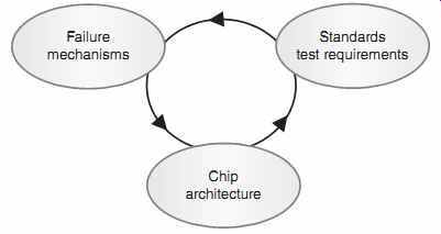
FIG. 11 Failure mechanisms, standards, and chip architecture
Failure mechanisms Chip architecture Standards test requirements
-----------
A second common ESD failure was associated with signal pin to signal pin. ESD standards required "pin-to-pin" testing to capture the failure mechanism associated with the lack of a current path between two pins. ESD networks were added between power rails to allow current flow (e.g., bidirectional ground-to-ground ESD networks).
10.2 Relationship Between ESD Standard Pin Combinations and Chip Architecture
Over many years of learning and evaluation of ESD failure mechanisms associated with these ESD standard pin combinations, the semiconductor chip architecture evolved to provide current paths between power rails of different power domains. Circuit design architecture separated power rails to provide noise isolation, but this led to ESD failures. Hence, the evolution of the semiconductor chip industry was to "recouple" the power grids and introduce ESD circuits to eliminate failure mechanisms associated with the chip architecture.
11. System Level Characterization
In system level analysis, system level characterization tests exist for the evaluation of system products. System level testing continues to be a growing field to address EOS and ESD failures in systems [21, 24]. FIG. 12 provides examples of system level characterization tests.
12. Summary
In this section, an introduction was given to the world of ESD testing. This includes a survey of different ESD tests, test procedures, devices, ESD networks, elements, to current paths. This will prepare the reader for the future sections, which gets into specific tests in more detail.
In Section 2, one of the most important tests in the history of ESD testing is discussed. This section focuses on the HBM test, and in addition indicates many of the present and future anticipated changes that will occur on this test.
---------------------
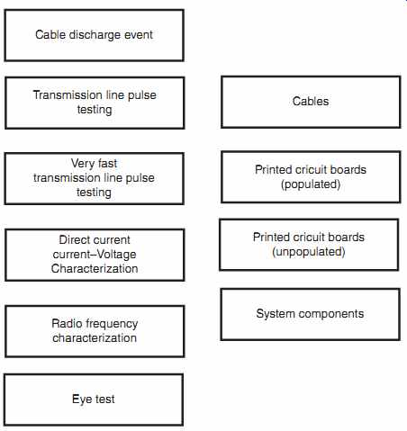
FIG. 12 System level characterization
Cable discharge event Cables Printed circuit boards (populated) Printed circuit boards (unpopulated) System components Eye test Radio frequency characterization Direct current current-Voltage Characterization Transmission line pulse testing Very fast transmission line pulse testing
--------------------
Exercises
1. How do people charge that leads to a spark at a metal door knob? Explain the triboelectric charging process. Are people capacitors? Where is the charge stored?
2. Explain the discharge process when a charged person touches a metal door knob or object.
3. Is the process of discharging the same all the time? What influences the discharge process? How many issues influence the discharge process? List at least four of them.
4. Why is repeatability and reproducibility important for establishing a standard test method? What if a method is not repeatable or reproducible?
5. What are the advantages of wafer level testing? List four variables.
6. What cannot be achieved on a wafer level? What are the issues?
7. What is the reason for component level testing? What does it provide for the foundry that produces them?
8. Does component level testing help system level developers? What it cannot provide?
9. How do you determine the ESD robustness of a technology? How do you quantify the ESD robustness of one technology generation to a second generation? How do you determine the effect of technology scaling?
10. If you were an ESD engineer in a foundry, how would you structure the entire business process for delivering semiconductor components? How do you protect the interest of your foundry? How do you protect the interest of the customer?
11. How does one take into account manufacturing variation and distribution versus ESD latent damage? Can you tell the difference?