AMAZON multi-meters discounts AMAZON oscilloscope discounts
The human body model (HBM) is the most widely established standard for the qualification and release of semiconductor components in the semiconductor industry. The HBM test is integrated into the qualification and release process of the quality and reliability teams for components in corporations and foundries. This section is dedicated to the HBM model.
The HBM standard is ANSI/ESD ESD-STM 5.1 - 2007 - ESD Association Standard Test Method for the Protection of Electrostatic Discharge Sensitive Items - Electrostatic Discharge Sensitivity Testing - Human Body Model (HBM) Testing - Component Level. Standard Test Method (STM) document, 2007.
The HBM is regarded as an electrostatic discharge (ESD) event, not an electrical overstress (EOS) event because it is charge transfer-related source, with a short pulse event. The model was intended to represent the interaction of the electrical discharge from a human being, who is charged, with a component, or an object. The model assumes that the human being is the initial condition. The charged source then touches a component or an object using a finger.
The physical contact between the charged human being and the component or object allows for current transfer between the human being and the object.
1. History
The HBM became of interest in early days in the mining industry in the 1950s. In the Bureau of Mines, investigation reports discussed the issue of electrostatic in the mining industry. A first publication was by P.G. Guest, V.W. Sikora, and B.L. Lewis as the Bureau of Mines, Report of Investigation 4833, U.S. Department of Interior, January 1952. A second article of interest was published by D. Bulgin, referred to as D. Bulgin. Static Electrification. British Journal of Applied Physics, Supplemental 2, 1953. Additional articles were published during this time frame.
An early investigator of issues with the HBM standard was T.M. Madzy and L.A. Price II of IBM in 1979 discussed a test system titled "Module Electrostatic Discharge Simulator". This article discussed that the ESD simulator was used within IBM since 1974. In 1980, H. Calvin, H. Hyatt, H. Mellberg, and D. Pellinen proposed values for the resistance and capacitance for the human ESD event for the finger tip and field-enhanced discharges in "Measurement of Fast Transients and Application to Human ESD," published in the 1980 Proceedings of the EOS/ESD Symposium. The proposed resistance for the finger tip was averaged 1920 ohm and capacitance of 110 pF, whereas the field-enhanced discharge was a resistance of 550 ohm and 120 pF. In 1981, H. Hyatt, H. Calvin, and H. Mellberg investigated the human ESD event, published in the 1981 Proceedings of the EOS/ESD Symposium, titled "A Closer Look at the Human ESD Event." One of the first standards developed for the HBM was military standard MIL-STD 883B Method 3015.1 referred to as "Electrostatic Discharge Sensitivity Classification," published in January 1982.
In 1983, R.N. Shaw and R.D. Enoch of British Telecom Research Laboratories published one of the first publications on a programmable test equipment at the EOS/ESD Symposium, titled "A Programmable Equipment for Electrostatic Discharge Testing to Human Body Models." The test system shown in the publication comprises of a high-voltage power source, a series charging resistor for charging the 100 pF capacitor, a 1500 ohm series resistor, and a single mercury wetted relay switch.
2. Scope
The scope of HBM ESD test is for testing, evaluation, and classification of components and micro- to nano-electronic circuitry. The test is to quantify the sensitivity or susceptibility of these components to damage or degradation to the defined HBM test. The test is performed with the component in an unpowered state.
3. Purpose
The purpose of the HBM ESD test is for establishment of a test methodology to evaluate the repeatability and reproducibility of components to a defined pulse event in order to classify or compare ESD sensitivity levels of components.
4. Pulse Waveform
A characteristic time of the HBM event is associated with the electrical components used to emulate the human being. In the HBM standard, the circuit component to simulate the charged human being is a 100 pF capacitor in series with a 1500-Ohm resistor. This network has a characteristic rise time and decay time. The rise time is in the range of 17-22 ns. The characteristic decay time is associated with the time of the network, which is 150 ns. The pulse event is a single polarity event. To address HBM ESD qualification, the test is performed in both positive and negative polarity events. FIG. 1 is an example of a positive polarity HBM pulse event.
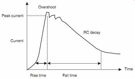
FIG. 1 Human body model (HBM) pulse waveform
HBM tests are performed in different pin combinations. Tests are performed between signal pin and referenced power rails. HBM test simulation also includes power-rail-to-power-rail testing, and signal-pin-to-signal-pin combinations. This is to evaluate all possible current paths for the ESD event. The HBM test standard of pulse waveform and pin combination are integrated into commercial HBM test systems.
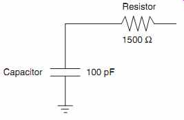
FIG. 2 Human body model (HBM) equivalent circuit model
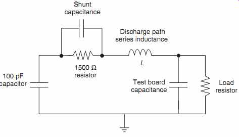
FIG. 3 Human body model (HBM) equivalent circuit model with parasitics
5. Equivalent Circuit
The HBM source can be represented as an equivalent circuit. FIG. 2 is a circuit schematic representation of the HBM source. The equivalent circuit can be represented as a capacitor element and a resistor element. In the HBM equivalent circuit model, the circuit component to simulate the charged human being is a 100 pF capacitor in series with a 1500-Ohm resistor. The capacitance represents the human body and the resistor represents the resistance of an arm.
The HBM source can include the parasitic elements as well as the load in the equivalent circuit. FIG. 3 is a circuit schematic representation of the HBM source including the parasitic elements and load. In the equivalent circuit, the 1500-Ohm resistor also has a parallel shunt capacitance. The discharge path also includes a series inductance. This element is followed by a test board capacitance and load resistance. The discharge path series inductance introduces damped oscillations in the waveform near the peak of the current.
6. Test Equipment
HBM commercial test equipment exists for the qualification and release of semiconductor components. FIG. 4(a) shows an example of an HBM source for an early commercial HBM test system. The HBM source comprises of a capacitor element and resistor element.
These are encased in an insulating material to avoid parasitic discharge to other test system components.
FIG. 4(b) shows an example of a second HBM source for another early commercial HBM test system. In these sources, the capacitor and resistor elements are modules that can be placed in the commercial tester.
HBM commercial test equipment will be required to release an HBM pulse to the device under test (DUT). The commercial test equipment must have a high-voltage source used to charge the HBM source circuit. A switch is contained within the test system that is closed when the high-voltage source charges the equivalent circuit. A second switch must be open during the charging of the HBM source circuit. The second switch is closed when the HBM circuit current is discharged into the load or DUT.
FIG. 5(a) shows an example of a present-day HBM ESD commercial test system. The system in the figure is the Hanwa S5000R HBM test system. This test system is a 128- and 256-pin count package level system. The test system meets the JEITA, ESDA, and JEDEC international standards. This test system can test other ESD models (e.g., machine model (MM) and small charge model).
FIG. 5(b) shows an example of a second HBM ESD commercial test system. This is the Hanwa HED-N5000 HBM tester for high pin count modules. This test system is a fully automated ESD test system with a pin count of 1056 pin sockets. This system can also test up to eight chips in parallel on a given test board.
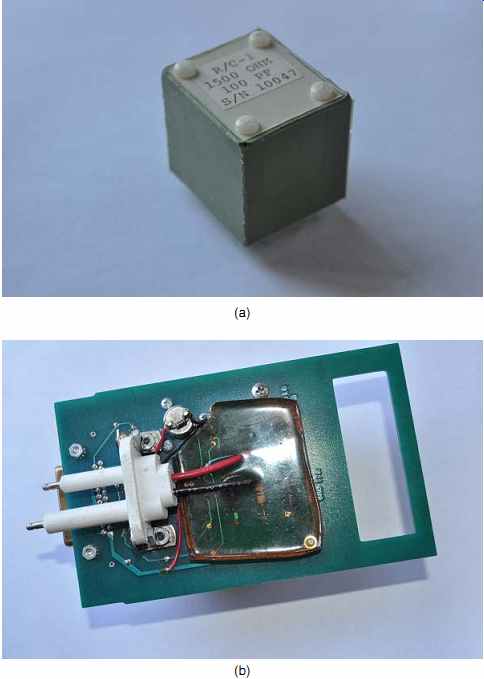
FIG. 4 Human body model (HBM) source
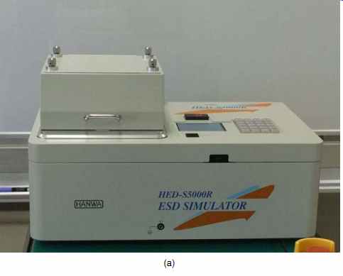
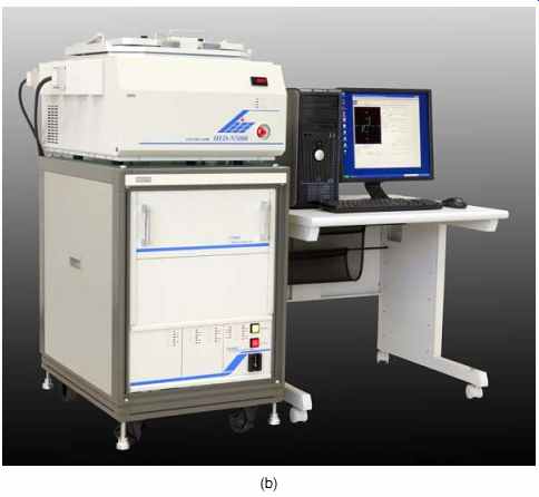
FIG. 5 (a) Human body model (HBM) commercial test system - Hanwa S5000R.
(b) Human body model (HBM) commercial test system - Hanwa HED-N5000
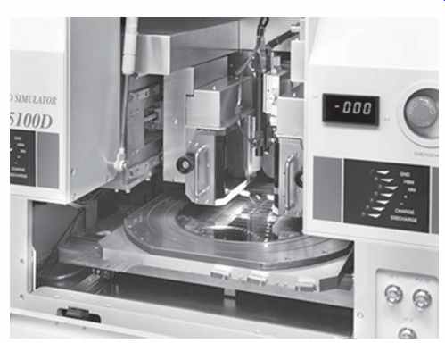
FIG. 6 Human body model (HBM) wafer level commercial test system
Human body commercial systems were first developed for qualification and release of semi conductor components. In the 1980s, there was no wafer level commercial HBM test system for semiconductor development, ESD library test and verification. In the semiconductor environment, it was important for development to have a faster process to evaluate ESD robustness of devices and circuits. Wafer level ESD characterization was possible by extending the wires from the socket to a wafer level work station and wafer probes.
Today, wafer level HBM test systems exist for development. FIG. 6 shows an example of a wafer level HBM ESD commercial test system.
7. Test Sequence and Procedure
In the testing of components, the commercial test systems have a defined test sequence and procedure. FIG. 7 provides a test sequence flow for the commercial HBM test systems.
In the testing of components to large increments for semiconductor device characterization, a grounded reference is established. An initial reading is performed prior to any applied voltage on the HBM source. A first step increment is defined on the capacitor element. All pins are pulsed with an ESD event, individually relative to the grounded reference. Each pin is evaluated based on a failure criterion (e.g., voltage shift, leakage). If the pin "passes," it remains in the test sequence for the next increment. Pins that "fail" are removed from the test sequence, where all other passing pins remain in the test sequence. The voltage is increased on the capacitor source to the next step level, and testing resumes for the surviving pins. In this case, after the desired steps are taken, the tester is stopped, and the failed pins versus surviving pins are recorded.
--------------------------
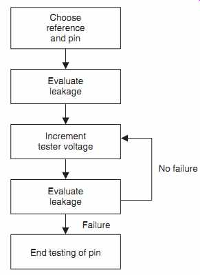
FIG. 7 Human body model (HBM) test sequence
Choose reference and pin Evaluate leakage Increment tester voltage Evaluate leakage No failure; Failure End testing of pin
-------------------------
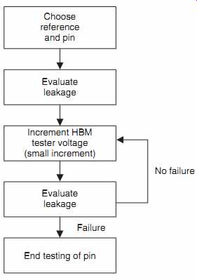
FIG. 8 Human body model (HBM) incremental step stress test sequence
Choose reference and pin Evaluate leakage Increment HBM tester voltage (small increment) Evaluate leakage No failure; Failure End testing of pin
------------------------
In the testing of components to small increments for semiconductor device characterization, a second test sequence is shown in FIG. 8. A first precheck of the pins is performed prior to charging the capacitor source. In small increment testing, a grounded reference is established. A first increment is defined on the capacitor element. All pins are pulsed with an ESD event, individually relative to the grounded reference. Each pin is evaluated based on a failure criterion (e.g., voltage shift, leakage). If the pin "passes," it remains in the test sequence. Pins that "fail" are removed from the test sequence, where all other passing pins remain in the test sequence. The voltage is increased on the capacitor source to the next increment level, and testing resumes for the surviving pins. This continues until all the pins have failed the failure criterion. In this methodology, with small increments, the actual failure level is determined for all the pins that are tested, with an accuracy associated with the increment step size.
8. Failure Mechanisms
HBM failure mechanisms are typically associated with failures on the peripheral circuitry of a semiconductor chip that are connected to signal pins. HBM failures can occur on the power rails due to inadequate bus widths and ESD power clamps between the power rails. HBM failures can occur in both passive and active semiconductor devices. The failure signature is typically isolated to a single device, or a few elements in a given current path where the current exceeded the capability of the element. ESD circuits are designed to be responsive to HBM pulse widths; this is an issue for EOS events since they are not "tuned" for EOS events. Specifically, the RC-triggered metal oxide semiconductor field effect transistor (MOSFET) ESD power clamp is designed for HBM events.
HBM ESD failures are also distinct from EOS events. HBM events will not typically cause failures in the package, printed circuit board (PCB), or single component devices mounted on a PCB.
FIG. 9 is an example of an HBM failure of a diode structure. Integrated circuit diode structures fail at the contact interface, silicon surface, or junction region.
FIG. 10 is an example of an HBM failure of a MOSFET structure. Integrated circuit MOSFET structures failure occurs from MOSFET source-to-drain, or at the MOSFET gate.
From HBM failures, typically, the failure is MOSFET source-to-drain failure.
FIG. 11 is an example of an HBM failure of a series cascode MOSFET structure.
Integrated circuit MOSFET structures failure in a series cascode structure can occur from the upper MOSFET drain to lower MOSFET source.
FIG. 9 Human body model (HBM) failure mechanism - diode failure
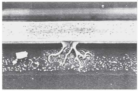
FIG. 10 Human body model (HBM) failure mechanism - MOSFET failure
FIG. 11 Human body model (HBM) failure mechanism - series cascode MOSFET
failure
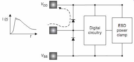
FIG. 12 Human body model (HBM) ESD event current paths - signal pin
to power (VDD)
FIG. 13 HBM ESD event current paths - signal pin to ground (V )
9. HBM ESD Current Paths
During ESD events, the current will flow from the signal pin that is pulsed to the grounded reference. FIG. 12 is an example of the ESD current path from the signal pin to the grounded reference VDD. In this case, the positive polarity ESD pulse leads to a positive current flow into the bond pad. The ESD current flows through the ESD p-n diode structure connected to the grounded reference VDD. Residual current also flows into the digital circuitry.
FIG. 13 is an example of the ESD current path from the signal pin to the grounded reference VSS. In this case, the positive polarity ESD pulse leads to a positive current flow into the bond pad. The ESD current flows through the ESD p-n diode structure connected to the power rail VDD. The ESD current continues to flow through the ESD power clamp between the VDD power rail and the VSS power rail. Residual current also flows into the digital circuitry.
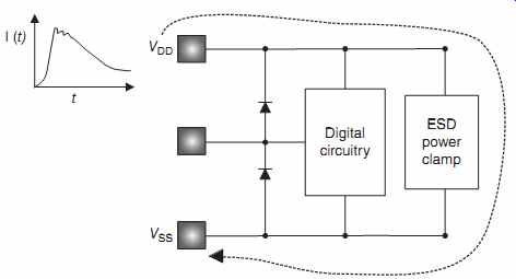
FIG. 14 HBM ESD event current paths - power rail (VDD) to power (VSS)
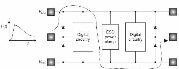
FIG. 15 HBM ESD event current paths - signal pin to signal pin within
a common power domain
FIG. 14 is an example of the ESD current path from the power rail VDD bond pad to the signal pin to the grounded reference VSS. In this case, the positive polarity ESD pulse leads to a positive current flow into the bond pad of the VDD power supply. The ESD current continues to flow through the ESD power clamp between the VDD power rail and the VSS power rail.
FIG. 15 is an example of the ESD current path from the signal pin to the grounded signal pin within a common power domain. In this case, the positive polarity ESD pulse leads to a positive current flow into the bond pad. The ESD current flows through the ESD p-n diode structure connected to the power rail VDD. The ESD current continues to flow through the ESD power clamp between the VDD power rail and the VSS power rail. Current flows through the ground rail, through the ESD p-n diode that is connected to the VSS rail, and the second grounded signal pin.
FIG. 16 is an example of the ESD current path from the signal pin to the grounded signal pin within an independent power domain. In this case, the positive polarity ESD pulse leads to a positive current flow into the bond pad. The ESD current flows through the ESD p-n diode structure connected to the power rail VDD. The ESD current continues to flow through the ESD power clamp between the VDD power rail and the VSS power rail of its own domain. Current flows through the "rail-to-rail" ESD network placed between the two ground rails. The current flows to the grounded reference rail.
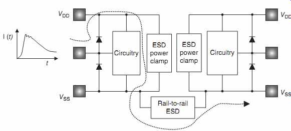
FIG. 16 HBM ESD event current paths - signal pin to alternate ground
rail domain to domain
FIG. 17 HBM signal pin ESD protection circuits - dual diode
10. HBM ESD Protection Circuit Solutions
FIG. 17 is an example of an ESD protection network known as a dual-diode network. The dual-diode ESD network is a commonly used network for complementary metal oxide semiconductor (CMOS) technology. A first p-n diode element is formed in an n-well region where the p-anode is the p-diffusion implant of the p-channel MOSFET device and the n-cathode is the n-well region connected to the power supply VDD. This is sometimes referred to as the "up diode." A second p-n diode element is formed in a p-well or p-substrate region where the n-cathode is the n-diffusion implant of the n-channel MOSFET device, or the n+/n well implant and the p-anode is the p-well region or p-substrate region connected to the power supply VSS. This is sometimes referred to as the "down diode." This circuit provides a "for ward bias" ESD protection solution for positive and negative ESD pulse events to the two power rails VDD and VSS.
An advantage of the dual-diode ESD network is that it is easy to migrate from technology generation to technology generation. In shallow trench isolation (STI) technology, this structure is scalable. A second advantage is that it has a low turn-on voltage of 0.7V. A third advantage is that it can be designed with low capacitance, making it suitable for CMOS, advanced CMOS, and RF technologies. A fourth advantage is that it does not contain MOSFET gate dielectric failure mechanisms.
FIG. 18 HBM signal pin ESD protection circuit - grounded gate NMOS (GGNMOS)
FIG. 18 is an example of a signal pin ESD network consisting of a grounded gate n-channel MOSFET device. The grounded gate NMOS (also referred to as GGN MOS) ESD network is a commonly used network for CMOS technology. Typically, it is an n-channel MOSFET whose MOSFET drain is connected to the signal pin and whose MOSFET source and gate are connected to the ground power rail. This circuit remains "off" in normal operation. When the signal pin exceeds the MOSFET snapback voltage, this circuit discharges to the VSS power rail. When the signal pin is below the ground potential, the MOSFET drain forward biases to the p-well or p-substrate region. An advantage of the GGNMOS ESD net work is that it is a natural scalable solution. As the technology scales, the MOSFET snapback voltage reduces, leading to an earlier turn-on of the MOSFET.
FIG. 19 is an example of a signal pin ESD network consisting of a silicon controlled rectifier (SCR) network. The SCR ESD network is a commonly used network for CMOS technology. An SCR is a four-region pnpn device. The p-anode is the p-diffusion implant of the p-channel MOSFET device and the n-cathode is the n-well region. A third region is the p-substrate, and the n-cathode is the n-diffusion implant of the n-channel MOS FET device, or the n+/n- well implant There are a large variety of pnpn structure that can be constructed, from high-voltage SCR (HVSCR),medium-voltage SCR (MSCR), to low-voltage trigger SCR (LVTSCR) structures. These can be constructed as single- or bidirectional net works.
FIG. 19 HBM ESD protection circuits - silicon controlled rectifier
FIG. 20 HBM ESD protection device - power rail to power rail protection
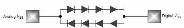
FIG. 21 Human body model (HBM) ESD protection circuits - ground-to-ground
network
FIG. 20 is an example of an ESD network that is placed between two power rails where the first power rail is a VDD power rail and the second power rail is a VSS power rail [62-64].
These types of networks are known as ESD power clamps. The most commonly used ESD networks are RC-triggered MOSFET ESD power clamps. This consists of a frequency trigger, a MOSFET drive stage, and an output MOSFET clamp device. The most commonly used network has a resistor-capacitor (RC) discriminator that is tuned to respond to an HBM ESD pulse event. The MOSFET drive stage consists of a series of inverter switches, with increasing width, to "turn-on" the output MOSFET clamp device. In recent years, these networks have been modified to respond to faster impulses, lower leakage, smaller area, and means to avoid false triggering.
FIG. 21 is an example of an ESD network that is placed between two ground rails.
ESD networks are placed between isolated ground rails to allow current flow between the grounds for signal pin-to-rail ESD testing where the signal pin is in a first domain, and the reference is contained in a second rail. In addition, it also assists pin-to-pin ESD HBM events and rail-to-rail HBM events.
11. Alternate Test Methods
Alternate test methods have been developed for HBM testing. FIG. 22 shows a picture of alternate test methods. In the mid-1990s, the pin count of semiconductor chips continued to increase beyond 1000 pins. Yet, ESD test systems' largest pin count was 250 pins. ESD test systems that exceeded 1000 pins were also not available. In addition, with the increased pin count, the test time continued to increase.
One method of testing was known as "split fixture" testing; one method had multiple fixtures mounted onto a single test board, and some corporations, "rotated" the chip in the smaller socket. Also in this time frame, "sample testing" was proposed to address the cost and time to test a high pin count semiconductor chip. To accelerate "ESD learning," wafer level testing was introduced to provide characterization of ESD networks, and circuits on wafer, instead of a packaged environment. In addition, two-pin testing is now growing to avoid the complexity of relay matrix-based test systems. Other methods will also be discussed, such as small step stress testing to transmission line pulse (TLP)-like HBM testing.
------------------
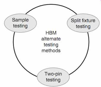
FIG. 22 Alternate test methods
Sample testing Split fixture testing HBM alternate testing methods Two-pin testing
-----------------
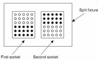
FIG. 23 HBM split fixture testing
First socket Second socket Split fixture
---------------
11.1 HBM Split Fixture Testing
Alternate testing methods were at time developed because the test system pin count did not keep up with the number of pins on a component. The socket of the test system was not large enough for socketing the component into the ESD test system. This problem occurred when semiconductor chips were at 1000 pin designs for microprocessors and CPUs, yet the highest pin count ESD test system was 250 pins. As a result, to test and socket some HBM test systems, "split fixtures" were developed to test all pins on the component. FIG. 23 is an example of a "split fixture."
11.2 HBM Sample Testing
As the number of pins increased on a semiconductor component, test time to test all pins on a component increased. As a result, it was proposed to introduce sampling methods to reduce the test time. With the increased pin count, the time to test an individual microprocessor was significant. With a large computer design system, which required eight semiconductor chips of 1000 pins each, this required a very large amount of test time. For example, in a 1000-pin semiconductor component, as many as 600 pins were the identical circuit. On testing this component, a Gaussian distribution of failures was observable. As a result, it is clear that by testing a smaller sample of "identical pins," the ESD robustness of the product can be qualified. The difficulty is the identification of "identical pins." FIG. 24 shows an HBM sample testing method.
11.3 HBM Wafer Level ESD Testing
To improve turnaround time of semiconductor development, wafer level characterization was introduced. FIG. 25 is an example of HBM wafer level test system. Wafer level testing can be used for ESD device characterization of active and passive elements in a technology library (e.g., resistors, capacitors, transistors) for ESD HBM technology benchmarking. Wafer level testing can be done on ESD networks that will be introduced into a technology ESD library. In addition, wafer level testing can be done on S-parameter extraction for RF technology library elements. HBM ESD testing of products can be done on a wafer to provide an early look prior to the first design pass.
---------------------------
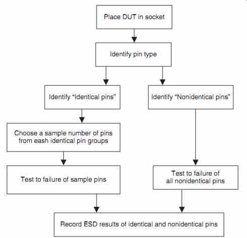
FIG. 24 HBM sample testing
Place DUT in socket
Identify pin type
Identify "Identical pins" Identify "Nonidentical pins"
Choose a sample number of pins from each identical pin groups Test to failure of sample pins
Record ESD results of identical and non-identical pins
Test to failure of all non-identical pins
----------------------------
11.4 HBM Test Extraction Across the Device Under Test (DUT)
One of the issues of the HBM test is that it does not provide the test engineer, ESD engineer, or circuit designer the true response of the pin under test. The HBM test only provides the survivability of the pin to the voltage level on the capacitor of the test system; this limits the insight what is possible to understand about the actual current-voltage (I-V) response of the signal pin. A test system can be developed as a wafer level test system that extracts the voltage and current across the DUT during the pulse event. Using a voltage probe, and a current probe, the signals can be transferred to a two-channel oscilloscope during a pulse event.
An HBM pulse can be generated by an RC-network source where the high-voltage supply charges the capacitor element, and a mercury wet switch can apply the pulse to the DUT.
When the pulse is applied, sampling of the current and voltage must extract the conditions across the DUT for evaluation of the results. This is performed in TLP testing by establishing a measurement window where the voltage and current are sampled and averaged. This technique has the disadvantage that the measurement window is not lat and leads to some error in the HBM extraction process (extraction is performed near the peak of the HBM pulse).
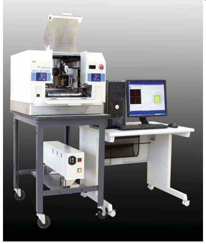
FIG. 25 Human body model (HBM) wafer level test equipment
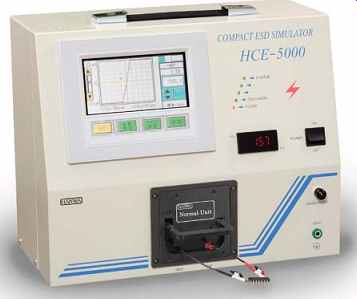
FIG. 26 Human body model Two-Pin test system (Hanwa Corporation)
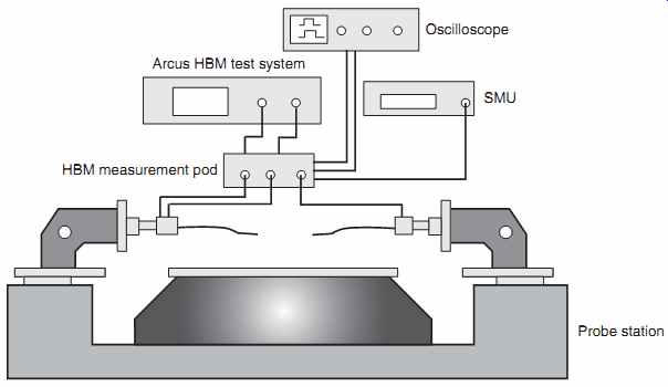
FIG. 27 HBM two-pin stress test equipment - Grund Technical Solutions
Arcus HBM wafer and device test system
12. HBM Two-Pin Stress
A present problem with HBM test systems is the relay systems used in the test system (FIG. 26). Relay-based HBM test systems have reached their limitation for test channels in high-pin-count components. HBM tester designs with test fixture boards (TFB), and relay matrices limit testing accuracy due to the pin-to-pin variations as well as pulse-to-pulse variations. Relay switching is used for selection of pin combinations that are required by the HBM standards. These relay systems have led to a significant amount of tester problems.
These problems include the following:
• Recharging pulse events
• Relay switching noise
• Pre-pulse spikes
• Trailing pulse events
• Switching relay parasitics
• Tester costs.
HBM two-pin (2-pin) testing has been more recently introduced into testing methods.
Two-pin testing can be done with packaged or unpackaged components. The advantage of two-pin testing is avoidance of the role of the switching matrix and socket on the HBM results. FIG. 27 is an example of a two-pin HBM test system, the arcus HBM wafer and device test system. The two-pin system eliminates the following [59]:
• Elimination of TFBs
• Elimination of test fixture board sockets
• Elimination of relay matrix.
FIG. 27 shows the test system with the arcus HBM test system, HBM measurement pod, SMU, oscilloscope, and wafer probe station. The test system reduces parasitics, eliminates anomalous stresses, avoids relay matrix problems, shortens test cycles, reduces cost, measures and verifies each pulse, and eliminates false failures.
12.1 HBM Two-Pin Stress - Advantages
There are a significant number of advantages using HBM two-pin testers. Two-pin testers provide the following:
• Improved HBM accuracy
• Improved testing flexibility
• Low parasitic
• Elimination of TFBs
• Elimination of test fixture board sockets
• Elimination of TFB parasitic
• Elimination of test fixture board trace coupling
• Elimination of relay matrix
• Elimination of false failures from DUT-relay matrix tester interactions
• Cost reduction due to elimination of test fixture board, sockets, and relay matrix.
12.2 HBM Two-Pin Stress - Pin Combinations
One of the problems with two-pin testing is that it does not fulfill all the requirements of pin combinations in today's standards established in relay matrix-based test systems [59]. In the future, a solution will be needed to allow acceptance of HBM two-pin testing. These may include the following:
• Elimination of the requirement of I/O to I/O pin combination requirement
• Optional requirement of I/O to I/O pin combination.
13. HBM Small Step Stress
A method of testing is the application of a small step stress in the qualification procedure. In many corporations, the testing is performed as a single increment to the specification level.
In the testing of components to small increments for semiconductor device characterization, a first precheck of the pins is performed prior to charging the capacitor source. In small increment testing, a grounded reference is established. A first increment is defined on the capacitor element. All pins are pulsed with an ESD event, individually relative to the grounded reference. Each pin is evaluated based on a failure criterion (e.g., voltage shift, leakage). If the pin "passes," it remains in the test sequence. Pins that "fail" are removed from the test sequence, where all other passing pins remain in the test sequence. The voltage is increased on the capacitor source to the next increment level, and testing resumes for the surviving pins. This continues until all the pins have failed the failure criterion. In this methodology, with small increments, the actual failure level is determined for all the pins that are tested, within an accuracy associated with the increment step size.
13.1 HBM Small Step Stress - Advantages
In this methodology, with small increments, there are a number of advantages as opposed to the method of a single increment.
A first advantage of small increment testing, is the avoidance of "ESD test windows." A disadvantage of a single value of ESD testing at the desired specification is, there are "ESD test windows" where the component can fail at a lower level. Some components may pass at a higher level but fail at lower levels. In this methodology, there are no "ESD windows" if the step stress has small increments.
A second advantage is that the actual failure levels of different pins and/or circuit types are determined. The actual failure levels of the different circuits can provide an understanding of the failure of specific circuits and which circuits are the "weak circuits." For example, in a microprocessor design, it was determined that the receiver network pin population was distinct from the off-chip driver (OCD) pin population.
A third advantage is that the recording of the failure levels of the component can provide quality control in a semiconductor manufacturing environment. Manufacturing semiconductor process shifts can be determined in a manufacturing line. An observed effect was epitaxial wafer control variations leading to ESD protection level variation. By knowing the protection level of specific pins, it was clear from the experimental data that there was a correlation of the ESD level versus well sheet resistance value. In a second example, silicide variation introduced ESD variation in ESD diode networks.
13.2 HBM Small Step Stress - Data Analysis Methods
In this methodology, with small increments, the statistical variation of the ESD pin population can be evaluated. By having the failure levels of all the pins, one can observe the Gaussian and non-Gaussian characteristics of the semiconductor chip ESD results. By having the experimental data for the mean ESD result, and the ESD level standard deviation, a complete understanding of the true robustness of the product chip can be determined.
13.3 HBM Small Step Stress - Design Optimization
In this methodology, with small increments, the statistical variation of the ESD pin population can be determined allowing for design optimization. By having the ESD failure levels of all the pins, semiconductor process experiments as well as layout improvements in design passes can be determined.
14. Summary
In this section, one of the most important tests in the history of ESD testing is discussed. This section focuses on the HBM test, and in addition indicates many of the present and future anticipated changes that will occur on this test. The changes include sample testing, rotation testing, to two-pin test methods. In the future years, there will be continued change and improvements in this test method.
In Section 3, the MM test is discussed. The MM purpose, scope, and waveforms are shown.
In addition, the discussion highlights the correlation between HBM and MM tests.
Exercises
1. Given a resistor of 1500 ohm and a capacitor of 100 pF, calculate the RC time of the human body model (HBM) event.
2. In semiconductor chip development, RC-triggered ESD circuits are designed to respond to the human body model (HBM) pulse waveform. Assume an ESD HBM pulse is a double exponential waveform, and determine what the RC time should be to protect the semiconductor chip. Assume a single RC time, 2× RC time, and 3× RC time.
3. Given the ESD HBM is an RC source and a switch. Assume the ESD pulse is discharged to a semiconductor chip of capacitance Cchip. Derive the current and voltage assuming the HBM capacitor is initially charged, the chip is uncharged, and the switch is then closed instantaneously.
4. Given the ESD HBM is an RC source and a switch. Assume the ESD pulse is discharged to a semiconductor chip of capacitance Cchip. Derive the current and voltage assuming the HBM capacitor is initially charged, the chip is precharged to a given value, and the switch is then closed instantaneously.
5. Given the HBM source has a high-voltage charging source, and a 1M-O resistor element to charge the HBM RC capacitor of 100 pF. The charging source is to be isolated with a switch when applying the ESD pulse to the chip. Assume the gas relay switch has a leakage current (e.g., a resistance), which prevents the full isolation of the charging source. What is the outcome? How does it affect the ESD testing results? What would the waveform look like before and after the RC capacitor is discharged (at the device under test)?
6. As mentioned in Problem 5, an ESD pulse is applied to a chip. The RC pulse is discharged and the next step increment pulse is ready to be applied. Assume that the charging source is not fully isolated from the semiconductor chip of capacitance Cchip. Calculate the voltage and current assuming the high-voltage source is at voltage 2000V, with a 1M-Ohm resistor and switch resistance of 100-Ohm.
7. Given that semiconductor chip has a large inductor load L, show the response of a chip to an RC-triggered circuit when testing VDD to ground. Show the RLC response. What inductance magnitude is an issue?