AMAZON multi-meters discounts AMAZON oscilloscope discounts
1. History
Electromagnetic compatibility (EMC) has been a concern from the beginning of power plants, power distribution, telephones, and electrical appliances. Power disturbances from lightning to switching electronics increased the issue of EMC. With the introduction of telephone, electrical noise suppression, noise coupling, and transient signals became a large issue.
This leads to a need for new devices and techniques for noise suppression.
With the introduction of radio technology, new EMC issues occurred. With broadband wireless telegraphs, interference from multiple sources occurred. The introduction of the vacuum tube oscillator made narrow-band radio communications possible and greatly reduced instances of unintentional electromagnetic interference (EMI) between radio transmitters.
Narrow-band radio transmitters enabled the transmission of voice communication resulting in the proliferation of commercial radio stations.
During World War IFI, radio frequency (RF) and microwave technology development accelerated. At MIT, in the "Rad Lab" radar and microwave devices were invented for radar development. Radio communications with both intentional and unintentional RF interference played a major role in the war. It was clear the importance of measuring, analyzing, and preventing EMC problems. This led to the development of procedures and standards for electromagnetic compatibility.
During WWII, the development of the atomic bomb led to another level of concern for military equipment during an atomic bomb ignition. A large electromagnetic pulse (EMP) event from an atomic bomb ignition led to the concern of the ability of military equipments to survive a harsh electromagnetic environment. It was this concern that accelerated the studying of the reliability and electrical overstress (EOS) of electronics in the late 1950s and 1960s. Driven primarily by the needs of the Cold War and the military, a new engineering specialization occurred for diagnosing, solving, or preventing EMC issues.
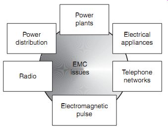
FIG. 1 Electromagnetic compatibility issues
In the 1960s and the 1970s, EMC became a large issue as the electronics were developed for single components to integrated circuit (IC) technology (FIG. 1). The initiation of the International Reliability Physics Symposium (IRPS) and the Electrical Overstress/ Electrostatic Discharge (EOS/ESD) Symposium occurred in the late 1970s. The early publications were associated with addressing concerns in EOS, ESD, EMP, and EMC.
2. Purpose
The purpose of EMC test is for the establishment of a test methodology to evaluate the repeatability and reproducibility of systems in order to classify or compare sensitivity or susceptibility levels of systems.
3. Scope
The scope of the EMC tests is for the testing, evaluating, and classification of systems. The test is to quantify the sensitivity or susceptibility of these components to damage, degradation, or disturbs to electromagnetic events.
• Printed circuit board (PCB)
• Populated PCB.
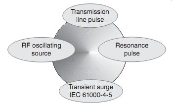
FIG. 2 Electromagnetic compatibility pulse waveforms
4. Pulse Waveform
For EMC evaluation, the pulse waveform can vary depending on the issue being studied. EMC evaluation can introduce the following pulse waveforms (FIG. 2):
• RF oscillating source
• Resonance pulse
• Transient surge
• Transmission line pulse (TLP)--square pulse.
RF oscillating sources have been used as early as the 1970s for the evaluation of the survivability of microwave electronics from an RF source. Resonance sources address the resonant coupling of an incoming electromagnetic source to a component, PCB, or system. Transient surge evaluation, such as the IEC 61000-4-5 pulse event, addresses the response of electronic coupling to a transient source. Additional surges such as combination wave, telecom wave, or ring oscillator wave can also be applied for EMC evaluation. Lastly, a square pulse event is used similarly to the TLP event for addressing electromagnetic coupling from a square pulse.
5. Equivalent Circuit
In the case of the EMC, the equivalent circuit is dependent on the type of source. The sources can be an RF oscillating source, single resonant frequency oscillating source, transient pulse to rectangular pulse events.
6. Test Equipment
Commercial test systems exist for EMC testing that can test a broad range of IEC immunity standards. The commercial test systems range from rack-mounted systems to new scanning methodologies. The following sections provide some examples of both the closed systems versus the scanning-based methodologies.
6.1 Commercial Test System
Commercial test systems exist for EMC testing that can test a broad range of IEC immunity standards. FIG. 3 shows a commercial product known as the EMC Pro Plus EMC Test System. The EMCPro Plus EMC Test System tests up to seven global EMC standards for susceptibility to EMI and EMC with a single instrument.
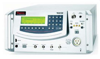
FIG. 3 Commercial EMC test system—EMC Pro Plus EMC (Thermo Scientific Fisher)
The Thermo Scientific EMCPro PLUS EMC Test System is an advanced, multi-capability, low-cost EMC immunity test system addressing a broad range of test capabilities and can be configured for testing to one or any combination of IEC basic immunity standards, such as the previously discussed IEC 61000-4-5. Additional function of this test system is as follows:
• Conducts surge testing with combination, telecom, and ring waves to IEC 61000-4-5 limit (6 kV)
• Performs electrical fast transient (EFT) testing to IEC 61000-4-4 limit (4 kV)
• Monitors surge voltage and current at the output terminals.
The test system addresses common surge requirements, such as combination wave, telecom wave, and ring oscillator wave requirements.
6.2 Scanning Systems
In recent years, scanning systems for EMC have been introduced. New method and test systems have been developed to analyze EMC that are either in development or are in commercial products.
EMC/ESD scanning is a method developed to determine the susceptibility or upsets of systems, circuits, and components to ESD or other EMC events without causing hard failures. In order to provide visualization of the EMC/ESD sensitivity, a localized source and means of scanning over the system is important to evaluate the local system or circuit response.
An ESD/EMC scanning system has been developed that produces a localized E-field or H-field, scans the equipment under test (EUT), and monitors the product for disturbs or upsets.
This test can scan exterior of products, subassemblies, and boards. The same test can be applied to components within the system (e.g., semiconductor ICs). In both cases, a mapping can be produced that overlays the system to determine entry points of electromagnetic noise and system sensitivity.
FIG. 4(a) shows an example of a high-level diagram for a scanning system. The test system comprises the following:
• Test table or fixture
• Pulse or waveform source
• X-Y scan control system
• Scanning armature
• Signal processing equipment and software.
In the figure, the example of the pulse source shown is a TLP source used to generate a local EMP event. The scanning armature sweeps across the EUT and is driven by the motor driver electronics. The data are collected and stored in the computer.
FIG. 4(b) shows a photograph of a small commercial scanning system. FIG. 4(b) shows the armature for pulsing the event. The armature position is initiated by the supporting mechanical system.
FIG. 5 is a photo of the Amber Precision Instrument full scanning system. The EUT is placed under the armature. A mechanical arm sweeps the source over the EUT driven by the motor drive circuitry. The pulse armature is connected to a pulse source that initiates the EMC event. The system also has voltage sources for powering the EUT during testing. The computer collects the information from the EMC test.
7. Test Procedures
In the following section, test procedures for ESD/EMC scanning system are discussed.
7.1 ESD/EMC Scanning Test Procedure and Method
FIG. 6 illustrates a flowchart of the ESD/EMC scanning system test procedure. The procedure starts by applying a stimulus to the EUT. If no "upset" occurs, the armature moves to the next test location. If an upset does occur at that location, the system reduces the test level to the lowest value. At the lowest pulse level if there is an upset, then the system moves to the next test point. If there is no upset at the lowest level, the system increases the test level, until an upset does occur. Once the upset level occurs, then the armature moves to the next test point and repeats the process at the next location. This process continues until the entire area of the EUT is completed. In this fashion, a plot of all the sensitive areas is obtained.
8. Failure Mechanisms
FIG. 4 (a) EMC/ESD high-level diagram (Reproduced with permission of Amber Precision Instruments). (b) EMC/ESD scanning system--small system (Reproduced with permission of Amber Precision Instruments)
For EMC testing, the failure of the system can be destructive or nondestructive. For the destructive failure, the failure can be the following:
• Component signal input parametric shift
• Component signal input permanent damage.
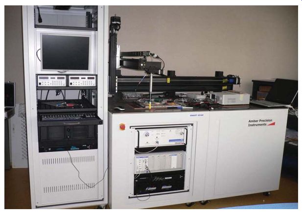
FIG. 5 EMC/ESD scanning system--large system (Reproduced with permission
of Amber Precision Instruments)
For the nondestructive failure, the failure can be the following:
• System disturbs
• System interrupts
• System timing delay.
EMC failures can be nondestructive event. System disturbs, interrupts, or time delays can lead to a system failure.
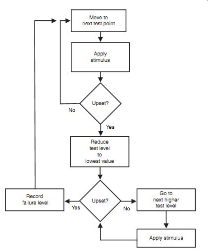
FIG. 6 ESD/EMC scanning test procedure
9. ESD/EMC Current Paths
EMC failures can be destructive or nondestructive events. EMC failures can occur in the component's internal circuitry, the component packaging, or in the PCB.
EMC current that lows into a component can be destructive if the current level exceeds the failure level of the bond pad, interconnects, ESD network, or internal circuitry. In the case where the current lows through the circuitry, and no destructive ESD current occurs, the return current low through the chip substrate can lead to a disturb, interrupt, or timing delay in the component.
EMC current that lows into a PCB trace can be destructive if the current level exceeds the failure level of the PCB trace or materials. The return current low through the PCB can also lead to a system disturb, interrupt, or timing delay. Given that the return current of a digital component lows under an analog component, system disturbs can occur.
FIG. 7 is an example of an EMC failure associated with the return current of a digital component lows under an analog component mounted on a common PCB.
10. EMC Solutions
PCB design can influence the sensitivity to EMI and provide good EMC characteristics. Today, PCB design is done with electronic design automation (EDA) tools. The EDA PCB design process undergoes the following steps:
• Circuit schematic: Schematic capture is achieved using an EDA.
• Card dimension: Card dimension and template size are determined for the application. This is based on the component sizes and heat sinks.
• Number of design levels: The number of the design layers is determined based on designer's designation or requirements. Decisions include the following:
• Power plane
• Ground plane
• Signal plane
• Trace line impedance: Decisions are made of the dielectric layer thickness copper routing thickness and trace width.
• Component placement: The placement of the components on the PCB is decided based on power distribution and physical dimensions.
• Signal trace routing: Signal lines are created using a "place and route" function.
• File generation: A Gerberile is generated for the final design.
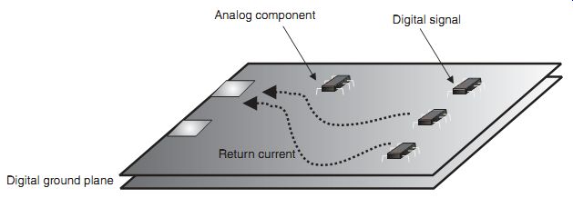
FIG. 7 EMC current paths--the return current
In the design of the PCB, a number of the design steps can influence the EMI and the EMC characteristics:
• Card dimension
• Number of design levels
• Power plane design
• Ground plane design
• Signal plane design
• Trace line impedance
• Copper routing thickness
• Trace width
• Component placement
• Signal trace routing.
Within this subject, guidelines can be created to minimize the systems' sensitivities.
11. Alternative Test Methods
Alternative test methods exist for a variety of different EMC issues. In this section, alternative methods are discussed, as well as the concept of susceptibility and vulnerability of electronics to EMC.
11.1 Scanning Methodologies
For evaluation of system level susceptibility and vulnerability, new methodologies have been developed that provide scanning of populated PCB [46-57]. The different types of PCB scanning include the following methods (FIG. 8):
• ESD/EMC immunity scanning method
• EMI emissions scanning method
• RF immunity scanning method
• Resonance scanning method
• Current spreading scanning method
• Current reconstruction scanning method.
11.2 Testing--Susceptibility and Vulnerability
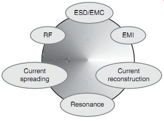
FIG. 8 Scanning methodologies
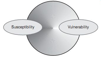
FIG. 9 Susceptibility and vulnerability
For the understanding of system failure, these scanning methods provide information about a system's susceptibility and vulnerability (FIG. 9). In this section, the distinction is high lighted.
Susceptibility is a system's sensitivity to "upset." Susceptibility may be a nondestructive event. Electrical currents that low on the PCB generate electromagnetic (EM) signals that can disrupt operation of a system. The electrical currents can low into the semiconductor components through the signal pins, power pins, as well as the power plane and ground plane With the presence of transient voltage suppression (TVS) devices on the PCB, EOS event current can be shunted to a power or ground plane [53]. Prior to the EOS protect devices, the current will generate EM emissions along the PCB trace. In addition, a "residual current" can also low into the semiconductor components beyond the EOS protection networks.
Scanning methods will provide a mapping of the susceptibility of regions of a PCB to electromagnetic emissions. As will be discussed, susceptibility is a measure of the PCB or components to the EM events. But, not all methods demonstrate actual "events" that enter the PCB traces, or components. Hence, a new method provides both susceptibility and vulnerability to EOS events.
11.3 EMC/ESD Scanning--Semiconductor Component and Populated Printed Circuit Board
EMC/ESD scanning can be performed on the semiconductor component and on a populated PCB. EMC scanning can be performed on an unpopulated or a full populated PCB.
12. EMC/ESD Product Evaluation--IC Prequalification
EMC/ESD scanning can be used for product evaluation. As an IC prequalification, EMC/ESD can be used as part of a qualification process. This can be completed in the design phase, or in a reliability evaluation.
13. EMC/ESD Scanning Detection--Upset Evaluation
EMC/ESD scanning methodology can be used for upset evaluation. By applying an EMI event, evaluation of the susceptibility of a populated PCB can be initiated and determine the upset sensitivity across a system.
13.1 ESD/EMC Scanning Stimulus
FIG. 10 illustrates an ESD/EMC scanning stimulus. Scanning systems can include EMI scanning, local H-field scanning, fixed resonant RF sources, and variable frequency scanning methods.
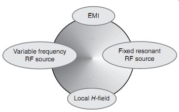
FIG. 10 ESD/EMC scanning stimulus
14. EMC/ESD Product Qualification Process
EMC/ESD qualification process flowchart is shown in FIG. 11. The qualification process should include the ESD device qualification for human body model (HBM), machine model (MM), and charged device model (CDM). If the component passes the standard ESD qualification, then evaluation of the device susceptibility scanning using standard test boards is completed. If it passes the susceptibility scanning process, the next step is the full system EMC compliance testing. If the system EMC compliance testing does not pass, then the susceptibility scanning at the system level is required to identify the problem areas [31, 32].
14.1 EMC/ESD Reproducibility
In order for a test method to achieve the status as a standard test method, it is important that the test method is both repeatable and reproducible. FIG. 12 shows an example of the susceptibility mapping from the same component under the same test. From the mapping, it can be observed that the same regions of the test show comparable susceptibility [31, 32].
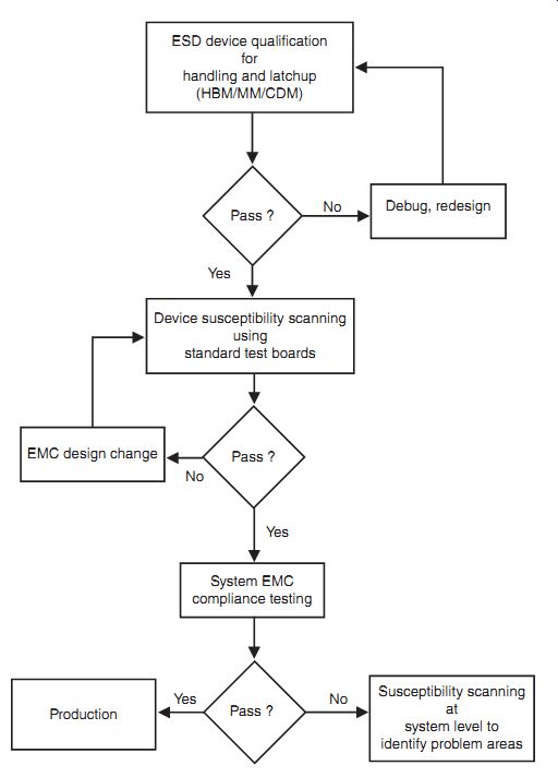
FIG. 11 ESD/EMC qualification process
14.2 EMC/ESD Failure Threshold Mapping and Histogram
The results can be displayed in a failure threshold mapping and in a histogram. FIG. 13(a) shows the EMC/ESD failure threshold mapping, and FIG. 13(b) shows an example of the display in histogram form. FIG. 13(a) shows the output failure threshold mapping that are sensitive regions. The test system clearly identifies a two-dimensional mapping of the areas of concern. The second plot displays a histogram of the voltage magnitude across the device.
14.3 ESD Immunity Test--IC Level
The scanning methodology can be used as a comparative ESD immunity tool. The scanning tool can be used to identify which pins are sensitive to noise. The failure levels of components can be evaluated by determining the failure frequency. A mapping of the test is shown in FIG. 14(a). FIG. 14(b) and (c) is an example of the pin response and failure levels.
After the scanning process, the system produces a mapping of the susceptibility overlaid on the physical image of the board or components. FIG. 14(d) shows a product sensitivity mapping of two products on the same system. It can be observed that the image mapping on the left (vendor A) is more sensitive compared to the image mapping on the right (vendor B). Although both fulfill the same electrical functional specification, their sensitivity to EMI is not equivalent.
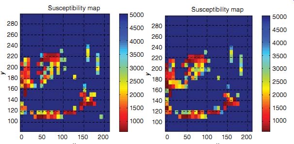
FIG. 12 ESD/EMC comparison of reproducibility
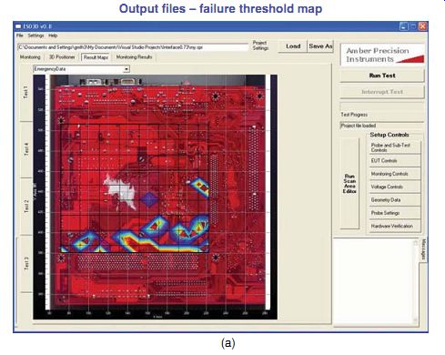
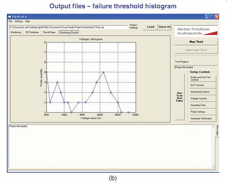
FIG. 13 (a) ESD/EMC failure threshold mapping (Amber Precision Instruments).
(b) ESD/EMC failure threshold histogram (Amber Precision Instruments)
14.4 ESD Immunity Test--ATE Stage
ESD immunity test can be initiated at the automatic test equipment (ATE) stage. At the ATE stage, evaluation of the ESD immunity can be performed with a manual scan process. The manual process can apply pulse events, or noise on the sensitive component that is mounted on the board. System tests can be performed that verify "system disturb" errors instead of hard failure of components. FIG. 15 shows an example of the error message associated with the failure of the signal. The ATE test system verified that the scan failure was reproduced on multiple parts.
15. Alternative ESD/EMC Scanning Methods
A methodology is needed for both component and system level manufacturers to test for susceptibility of both the components and the systems and have a means to correlate the relationship. A susceptibility test that can correlate system level upsets and the location of the upset is key to building better systems.
Today, component ESD models, which are unpowered, cannot provide enough information to estimate the performance at a "powered" state of the system.
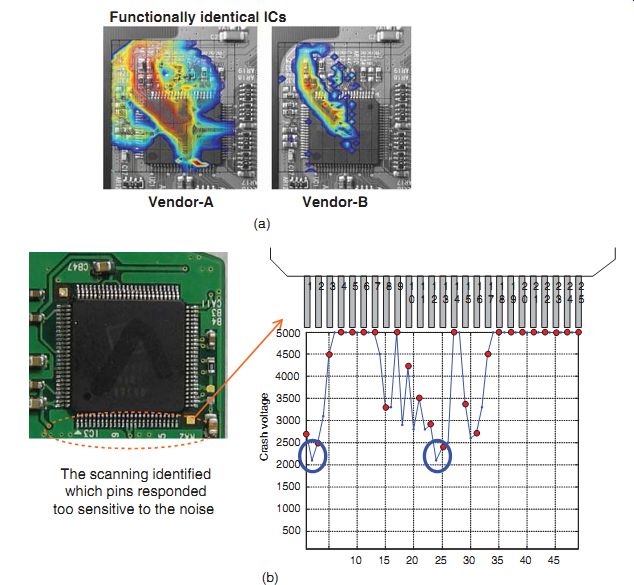
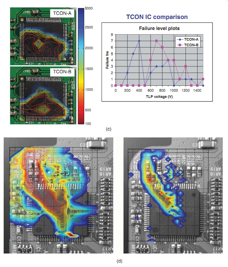
FIG. 14 (a) ESD immunity IC level. (b) ESD immunity IC pin response.
(c) ESD immunity IC pin failure levels. (d) ESD/EMC image comparison (vendors
A and B).
15.1 Alternative ESD/EMC Scanning Methods--Printed Circuit Board
In a PCB, motherboards, and the components itself, the ability to determine where the susceptibility problem occurs is very important. With the complexity of computer chips, and the spatial extent of the system board, it is very important to determine exactly where the problems occur in order to improve and ix the problems. One of the biggest problems today is that there is no visualization capability of the location of the susceptibility concern. As a result, EMC susceptibility improvements are evaluated by relying on both trial-and-error experimentation and EMC experience.
This ESD/EMC scanning system can apply different stimulus sources. The pulse test can be an RF source, EFT, transmission line, or ESD gun. A TLP source can be used to provide a TLP or very fast transmission line pulse (VF-TLP) event. For simulation of system-like events, the human metal model (HMM) or IEC 61000-4-2 test can be applied.
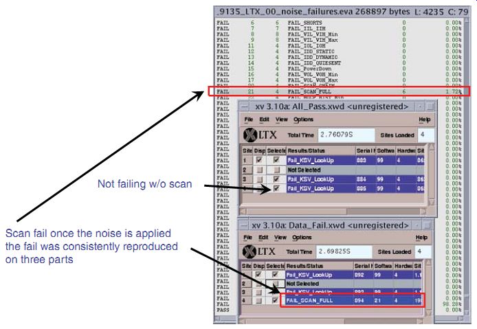
FIG. 15 ESD immunity at ATE stage
FIG. 16 is an example of the scanning results from a motherboard. In the image map ping, there are regions of sensitivity. With this mapping, it provides guidance for potential redesign of the motherboard.
With this EMC/ESD scan system, components and system boards can be evaluated in the design phase, assembly, or for qualification. A convergence of system level and chip level ESD testing is occurring today with these new methodologies.
15.2 Electromagnetic Interference (EMI) Emission Scanning Methodology
In the ESD/EMC method discussed earlier, current was injected into the current probe to generate a magnetic field to couple the populated circuit board to determine the susceptibility. The probe was then swept across the entire sample to provide a mapping of susceptibility.
Another methodology is the EMI emission scanning method [45-50]. In this method, the PCB is powered, and operable, and the probe is used in a "listening mode" where it is mapping the electromagnetic emissions on the PCB sample. This method is valuable for evaluation of the regions of the PCB that are sources of electromagnetic emissions.
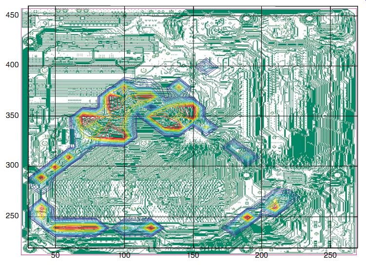
FIG. 16 Motherboard image scan (Reproduced with permission of Amber
Precision Instruments)
15.3 Radio Frequency (RF) Immunity Scanning Methodology
A method to determine the sensitivity and susceptibility of RF signals can be achieved using an RF immunity scanning method [48-50]. Using an RF source, an RF signal can be connected to a scanning probe. The populated PCB or motherboard is then powered and cycled. The RF signal can be scanned over the populated PCB and system level upsets can be evaluated.
15.4 Resonance Scanning Methodology
A method to determine the sensitivity and susceptibility of resonant frequency signals can be achieved using a resonance scanning method. Resonant frequencies of the PCB, antennae, and components can be an issue. Using an RF source, a signal may be applied to the scanning probe to evaluate the effect of a resonant signal across the PCB.
15.5 Current Spreading Scanning Methodology
In the prior methodologies, the scanning probe was established a signal across the populated PCBs to determine the relative susceptibility of different regions. The scanning process provides insight into potential regions where a PCB and components can be sensitive to electromagnetic emissions, RF signals, and resonance states. The sensitivity mapping can assist the system developer to determine which component to choose by determining susceptibility of equivalent components. It can also determine potential weak spots in a motherboard design where EMI, RF, noise, and other signals may enter a system.
16. Current Reconstruction Methodology
For EOS, the influence on the system is a function of both the low of current from the signal and power connections, and the sensitivity of the regions that they influence. Hence, susceptibility mapping does not provide the actual vulnerability of the system.
By injecting EOS events into the ports, and connections, the current will low into the sys tem. As the EOS event is injected into the PCB, the trace signal will generate E- and H-field emissions. Using the scanning probe, the emissions from the injected EOS current can be mapped and determine where the current lows in the network [53].
16.1 EOS and Residual Current
FIG. 17 shows an example of a PCB with a component chip mounted. An EOS on-board protection device is shown on the PCB. The EOS current is injected into the system, where a large percentage of the pulse event lows through the EOS protection device. In the scanning system, the current low can be mapped from the E- and H- fields generated using the scanning probe, as the signal or power pin is pulsed.
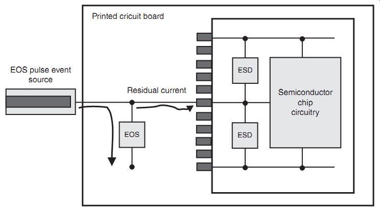
FIG. 17 EOS and residual current
16.2 Printed Circuit Board (PCB) Trace Electromagnetic Emissions
FIG. 18 demonstrates a populated PCB and the electromagnetic emissions coming from the signal traces. In the plot are incoming signals that are electrically connected to resistor elements in series with a chip. Measurements show the EM emissions from the pulse event prior to the resistors and after the chip. Results show that only a small percentage of the EM signal exits the semiconductor chip, showing the influence of the resistor in lowering the cur rent entering the semiconductor chip during an ESD event.
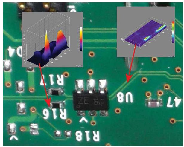
FIG. 18 Printed circuit board trace electromagnetic emissions (Pragma
Design)
16.3 Test Procedure and Sequence
FIG. 19 is a susceptibility scanning flowchart of the process. In the process, a pulse train is injected into the system. The device under test (DUT) is observed where the failure level is recorded. After this is achieved, the probe is shifted to a new location and the process is continued until a full mapping is achieved [31, 32, 53].
FIG. 20 highlights a comparison of three signals produced from the current reconstruction methodology. FIG. 21 shows a populated PCB using the scanning methodology.
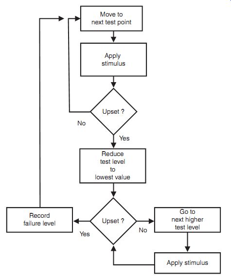
FIG. 19 Current reconstruction--test procedure and sequence
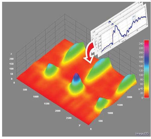
FIG. 20 Printed circuit board emissions (Reproduced with permission
of Pragma Design)
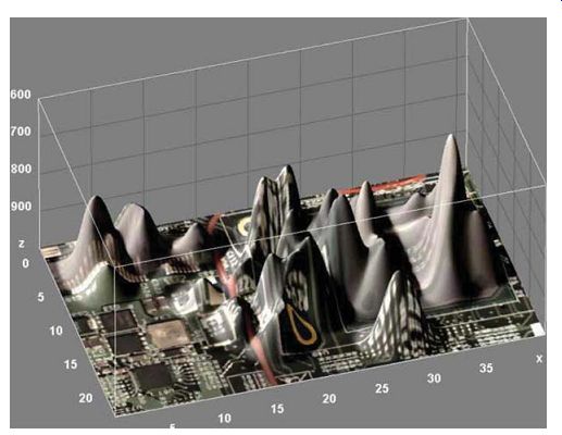
FIG. 21 Printed circuit board emissions (Pragma Design)
17. Printed Circuit Board (PCB) Design EMC Solutions
There are many decisions in the design of PCBs that influence the EOS, EMI, and EMC sensitivities. The component selection and placement influences these issues. Some guidelines for printed circuit design for placement and component selection are as follows:
• Component placement and ESD return current: Components should avoid being placed over ESD return current ground traces.
• Connector edge placement: Connectors should be located on the same edge of a PCB.
• Connector corner placement: Connectors should be located on one corner of a PCB if possible.
• Common connector: All off-board signals from a single device should be routed through a common connector.
• Connector to on-board I/O components spacing: Components connected to I/O nets, connectors, and off-board components should be located within 2 cm away from connectors.
• Connector and I/O to on-board non-I/O components spacing: Components not connected to I/O nets or connectors should be located 2 cm away from I/O nets and connectors.
• Digital component off-chip transition timing: Digital components should be selected to have a maximum off-chip rise and fall times.
• Clock and clock oscillator placement: Clock drivers should be located within proximity of clock oscillators.
Trace routing and power/ground plane decisions are key to avoid EMI, and EMC concerns.
Some guidelines for printed circuit design for signal traces are as follows:
• Power trace width: All power supply line traces should be of suitable width for EOS robustness objectives.
• Ground trace width: All ground line traces should be of suitable width for EOS robustness objectives.
• Signal trace width: All signal line traces should be of suitable width for EOS robustness objectives.
• Critical signal trace placement: Critical signal traces should be placed between power and ground planes. This avoids susceptibility of noise, EMI, and other sources.
• Critical signal trace placement and ESD return current: Critical signal traces should avoid being placed over ESD return current ground traces.
• Non-I/O trace placement: Traces that are not I/O should not be located between an I/O connector and a device that receives or sends signals using that connector.
• Non-I/O trace placement and I/O components: Signals with high-speed contents should not be placed under components that contain I/O components.
• Signal trace and power plane separation: No trace should be used for connection to the power plane.
• Signal trace and ground plane separation: No trace should be used for connection to the ground plane.
• I/O to connector trace length: Trace lengths from I/O to connectors should be minimized.
• High-speed digital trace length: Trace lengths for high-speed digital signals should be minimized.
• Clock trace length: Trace lengths for clocks should be minimized.
• High-speed trace to board edge: High-speed traces should be routed at least 2X from the board edge, where X is the distance between the trace and its return current.
• Differential signal trace pairs: Differential signal trace pair should be routed together and maintain same distances from adjacent shapes, objects, and solid planes.
Some guidelines for printed circuit design for power planes are as follows:
• Power plane and traces common layer: Power planes and traces should be routed on the same layer.
• Power plane--power return plane (ground) common layer: All power planes that are referenced to the same power return plane should be routed on the same layer.
FIG. 22 shows an example of a design methodology to optimize a PCB for EMC. The methods of the design include identifying (1) EMI sources, (2) critical paths, (3) antennas, and (4) coupling mechanisms. Using the scanning methodologies, these issues can be evaluated and quantified.
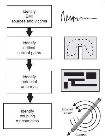
FIG. 22 Printed circuit board design
18. Summary and Closing Comments
This section addressed EMC as well as EMI as an introduction to many of the new state of-the-art methods. In the present and the future, the direction of EMC and EMI analysis will take on the process of EMC scanning methods to pinpoint the location and susceptibility of components. It will also be used to evaluate competitive analysis and choosing vendors to provide the best designs and best systems in the future. In the coming years, new methods will be developed, and some methods will be shown to be advantageous over others. It will be interesting in the future how this field of interest will evolve.
Problems
1. Describe electromagnetic compatibility (EMC). How do you define it? How wide is the scope?
2. Describe electromagnetic interference (EMI). What technologies is this an issue?
3. Magnetic recording heads outside of the disk drive can fail from electromagnetic interference (EMI). Explain the process of failure.
4. Describe susceptibility.
5. Describe vulnerability. How does vulnerability differ from susceptibility?
6. Describe what the scanning process signal demonstrates.
7. Describe what the current reconstruction process demonstrates.
8. Explain the distinction of the ESD/EMC scanning from the current reconstruction process.
9. Describe how the TLP is used for the scanning processes versus the current reconstruction process.
10. How will these test methods change system engineering and quality of future products?
References
[not listed]