AMAZON multi-meters discounts AMAZON oscilloscope discounts
1. History
Electrical overstress (EOS) has been an issue with the coming of the electrical age, when electricity and electrical product were first introduced into the mainstream of society. With the introduction of electrical power systems, the telephone, and electronics, inventions such as circuit breakers and fuses became the first type of EOS protection concepts to avoid overload of electronic systems.
EOS has been an issue in devices, circuit, and systems for electronics for many decades, as early as the 1970s and continues to be an issue till today [6-12]. Market segments from consumer, industrial, aerospace, military, and medical are all influenced by this issue. The experience of EOS failures are occurring at the device manufacturer, supplier, assembly, and the field. In the electronic industry, many products and applications are returned from the field due to "EOS" failure. To make progress in addressing the EOS issue, it is important to provide a framework for evaluation and analysis of EOS phenomena. As part of this frame work, it is important to apply a vocabulary and definitions. It is key to apply both physical and mathematical definitions to quantify the EOS conditions. It is equally important to establish a methodology of failure analysis and testing. It is also critical to establish an awareness of the origins and sources of EOS concerns. In the end, to provide better EOS robust products, it is important to define design practices and procedures, as well as EOS control programs for manufacturing and production areas.
EOS sources exist from natural phenomena, power distribution, power electronics, and machinery. A significant natural phenomenon is lightning. Power distribution includes switches, cables, and other power electronics that can be a source of EOS. EOS sources also occur from design characteristics of devices, circuits, and systems. In the following sections, these issues are discussed.
Many of the EOS issues can occur from the design of the semiconductor component, the system, and its integration. Examples of EOS source design issues are as follows:
• Semiconductor process--application mismatch
• Printed circuit board (PCB) inductance
• PCB resistance
• Latchup sensitivity
• Safe operating area (SOA) power rating violation
• SOA voltage rating violation
• SOA current rating violation
• Transient SOA--di/dt and dv/dt.
Testing and test simulation of devices, components, and systems are an important part of the evaluation to EOS. EOS test simulation is valuable part of understanding EOS failures. EOS testing provides the following:
• Root Cause Analysis: Determining the root cause of component and system failures
• Replication of Failure: Repeat the visual and electrical signature
• Technology Hardness Evaluation: Determining the robustness (or hardness) of a technology
• Technology Benchmarking: Comparative analysis of EOS or electrostatic discharge (ESD) hardness technology-to-technology
• Component Reliability Qualification: Qualification and release of components
• System Qualification: Qualification and release of systems.
One of the key concerns of EOS is the cost. There are different types of costs associated with EOS. In this section, the cost associated with field returns is discussed. In order to quantify the cost of EOS events on products, it is critical to categorize what percentage of the field returns are in fact EOS related.
Product field returns occur in all electronic components independent of the technology generation and period of time of evaluation. One of the key difficulties in the semiconductor industry is the ability to track, record, and maintain a database of these field failures.
A key question in the electronic industry is: what is the percentage of the field returns that is due to EOS? In the mid-1980s, the military established an in-house program to track, record, and categorize field failures to answer this question. The U.S. military and the Reliability Analysis Center (RAC) in Rome, NY, jointly established the Field Failure Return Program (FFRP), with the objective of providing feedback to the semiconductor industry and determining the root cause of failure. By establishing the root cause of failure, the corrective action can be initiated. The FFRP goals were as follows:
• Identify high failure rate or component problems.
• Identify their root causes of failure from failure analysis.
• Feedback the information to the supplier, industry, or government organization for corrective action.
In this early reliability study, data from 24 different systems were collected and reviewed.
In this review, 1650 parts were evaluated, of which the part numbers were from actual field failures that were operational from 2 to 10 years. Table 1 shows the results of the field failure categories [1].
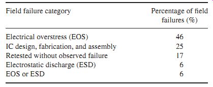
Table 1 Field failure categories and percentage
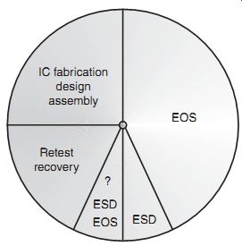
FIG. 1 Field failure categories
From this study, 46%of the field returns were associated with EOS. It was regarded from this study, a number of EOS issues were associated with poor system design, improper maintenance procedures, and improper operational procedures. In the second category, it was regarded that these failures were from inherent laws and latent defects. Of the field returns, only a few percent were related to ESD. Note, that in some cases, it was decided that it was not possible to determine if the failures were EOS or ESD (FIG. 1).
The results of this study are not significantly distinct from other future studies. It is typically quoted that EOS is a high percentage of field failures, and a certain percentage cannot distinguish from EOS or ESD.
In a more recent study by C. Thienel for the automotive industry called "Avoiding Electrical Overstress for Automotive Semiconductors by New Connecting Concepts" attributed 6% of the failures to ESD and 94%to EOS [7]. A large percentage of the fails were "no defect found" and approximately 32% were EOS/ESD failures.
2. Scope
The scope of EOS test is for the testing, evaluation, and classification of components and micro- to nano-electronic circuitry. The test is to quantify the sensitivity or susceptibility of these components to damage or degradation to EOS [1].
3. Purpose
The purpose of the EOS test is for establishment of a test methodology to evaluate the repeatability and reproducibility of components or microelectronic circuitry to a pulse event in order to classify or compare EOS levels of components [1].
4. Pulse Waveform
ESD event characteristic time response is associated with a specific process of charge accumulation and discharge. Hence, the characteristic time response is definable enough to establish an ESD standard associated with the specific process. Second, the time response of ESD events is fast processes. The time constant for ESD events range from sub-nanoseconds to hundreds of nanoseconds.
In contrast, EOS events do not have a characteristic time response. They can have short time response or long (note: today, it is popular to separate the "ESD events" as distinct from "EOS events" which is what will be followed in this text). EOS processes are typically slower, and distinguishable from ESD events by having longer characteristic times. The time constant for EOS events range from sub-microseconds to seconds (FIGs 2- 4).
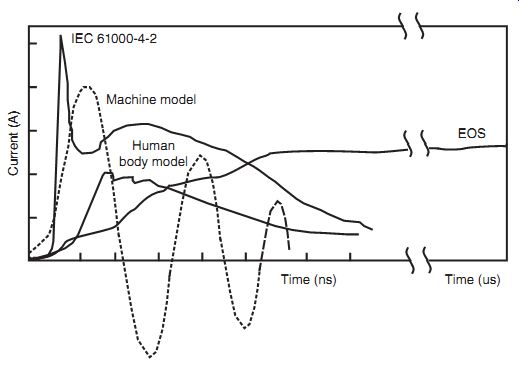
FIG. 2 EOS versus ESD waveforms
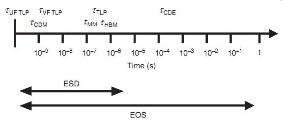
FIG. 3 EOS and ESD event time constant spectrum
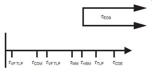
FIG. 4 EOS and ESD event time constant hierarchy
5. Equivalent Circuit
In EOS, there is no defined pulse width nor pulse shape. As a result, there is no equivalent circuit. What is known is that the time constant is long.
Today, there is discussion of a future EOS-defined pulse and equivalent circuit, which is a "long duration pulse transmission line pulse (LD-TLP)" of pulse width 500 ns. Given that this is an accepted pulse waveform, then the equivalent circuit would be a low loss transmission line.
6. Test Equipment
In EOS, there is neither defined pulse width nor pulse shape. As a result, there is no equivalent circuit. What is known is that the time constant is long. Using square pulse testing or oscillatory pulse events, EOS phenomena can be quantified.
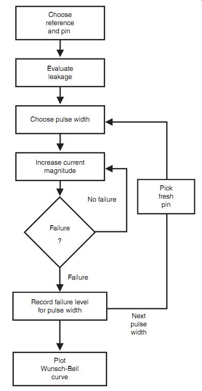
FIG. 5 Test procedure
7. Test Procedure and Sequence
In EOS, a test procedure and sequence can be defined to evaluate the EOS robustness.
FIG. 5 illustrates an example of a test procedure and sequence.
8. Failure Mechanisms
EOS failure mechanisms can occur from electrical overvoltage (EOV), electrical overcurrent (EOC), and electrical overpower (EOP) [1, 6, 13-71]. These conditions can lead to melted packages, blown single component capacitors and resistors, ruptured packages, blown bond wires, cracked dielectrics, fused and melted metal layers, and molten silicon.
Failure analysis of components and systems involves investigation, science, and experience.
As a failure analysis matures, a failure analyst's experience will allow a faster resolution of the root cause and solution. A failure analyst is like a forensic investigator who much finds the problem and resolves the case for each product failure. This is important in product development of semiconductor components where the answer will be required prior to undergoing the next "design pass." Time is limited between design passes to allow shorter cycles of the design for release and volume ramping into production.
The steps of the failure analysis process are as follows:
• Information gathering
• Failure verification
• Failure site identification and localization
• Root cause determination
• Feedback of root cause
• Corrective action
• Documentation reports
• Statistical analysis, record retention, and control.
8.1 Information Gathering
In the information gathering process for evaluation of EOS events, there are many elements to acquire and assemble to get a coherent view of the failure:
• Failure facility or field location: Where did the failure occur? Did it occur in manufacturing, production, or the field? In what stage of the process did this occur? What tools did the product undergo in manufacturing? What is the yield history of the different tools? In semiconductor manufacturing and assembly, there are yield analysis experts who know how to determine the path of the hardware and where yield losses occur. Yield experts will also have inspection history, and qualification of the tools, stations, and environment history.
• Failure determination method: How was the failure discovered? Is it important to determine root cause of how it was found? Thermal stress? Electrical measurements? Visual signature? Electrical characteristics?
• Visual signature: From visual inspection, is there any sign of the failure or defect? This is possible on the PCB, plastic molding (in the forms of discoloration, molten package, holes, and bubbles in the package).
• Electrical signature: From the electrical signature, what is the type of electrical signature? Short? Open? IDD leakage? I-V characteristic shift? VDD-VSS resistance?
• Product description and datasheet: Knowledge of the product description, function, and electrical parameters is important for the evaluation of the product. It is important to under stand the functional blocks in the physical design.
• Comparative study: It is valuable to evaluate examples of good product and compare the electrical response of good versus bad part numbers. For visualization of the electrical characteristics, it is a good practice to have the data overlaid, or together in a report.
• Database review: It is valuable to evaluate and review the product history in terms of temporal variation and statistical parameters. It is important to evaluate the site-to-site, wafer-to-wafer, lot-to-lot, and foundry-to-foundry differences within a manufacturing environment or assembly facility. This may provide a clue to the source of the problem.
• Electrical test simulation: A means to verify and re-simulate the event is important to see if the failure mechanism can be repeated and show the same electrical signature or visual signature. For example, a key question is to determine whether the event is ESD or EOS.
ESD tests (e.g., human body model (HBM), machine model (MM), charged device model (CDM), IEC 61000-4-2, HMM) can be performed to try to replicate the electrical and visual signatures. To determine if it is latchup, JEDEC latchup testing can be completed, where the current is increased to failure. For EOS, a series of electrical simulations can be performed for different current magnitudes and pulse widths.
8.2 Failure Verification
The goal of failure verification is to determine whether one can reproduce the failure. This can be completed by product test and retest. Retesting is important, since some failures recover, or never really occurred. A percentage of field returns at times never repeat the failure signature.
Comparative testing of good/bad product can also be performed for the verification process.
This can be done by overstress test simulation on untested or "good" parts.
Both nondestructive and destructive testing methods exist for failure verification. Non destructive testing methods are as follows:
• Optical inspection
• Acoustic microscope
• X-ray inspection
• Pin-to-pin testing
• Pin-to-rail testing
• Parametric functional testing.
8.3 Failure Site Identification and Localization
For the identification of the failure site within the system, this can be done by either visual external inspection or internal inspection. For visual inspection, one can look for the following visual damage signatures:
• Package lead damage
• Foreign material
• Cracks
• Package discoloration
• Corrosion.
For internal inspection, the following visual damage signatures are as follows:
• Melted metallurgy
• Cracked interlevel dielectrics
• Molten silicon.
8.4 Root Cause Determination
Root cause of the failure can be determined by evaluation of the manufacturing and production center records and processes, the electrical and/or visual signatures, evaluation of the circuit schematics and design layout, and test simulation. Once the root cause is determined, it is important to review the results and draw definitive conclusions.
8.5 Feedback of Root Cause
Once the root cause is determined, it is important to provide feedback to the manufacturing, production, design team, reliability, and quality teams. Results and conclusions should be reviewed with the complete team to close the issue and establish corrective actions.
8.6 Corrective Actions
Corrective actions can be taken to avoid repeating the event after its root cause is determined.
The corrective action can be the chip design (e.g., design layout and/or circuit), manufacturing tooling, or production processes. It is also important in the case of a corporation with a high "reuse" of circuit blocks, to prevent EOS-sensitive or ESD sensitive blocks from being used in other products until the corrective actions are completed.
8.7 Documentation Reports
Documentation of the results in a report is important for the EOS control program management.
To have a good EOS control program, documents may be a source of learning for future design reviews, checklists, procedures, and audits.
8.8 Statistical Analysis, Record Retention, and Control
Statistical analysis and record retention are important for an EOS control program and do maintain an EOS Safe Protected Area.
A common question that arises is: whether from the failure analysis can one determine if the root cause of the failure is EOS or ESD? Resolving this question is dependent on the visual failure signature.
There are certain categories of failures that ESD does not typically cause and EOS events do cause (FIG. 6). Failures that are typically caused by EOS phenomena but not ESD are as follows:
• PCB damage
• Package molding damage
• Package pin damage
• Wire bond damage.
Today, PCBs, packaging, and wire bonds do not typically fail due to an ESD event caused by HBM, MM, or CDM events. FIG. 7 is an example of a wire bond failure.
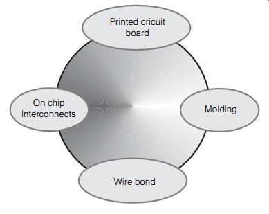
FIG. 6 EOS failure mechanisms
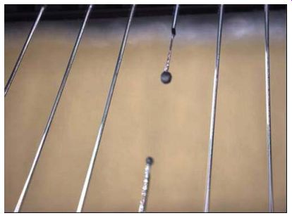
FIG. 7 EOS failure mechanism--wire bond
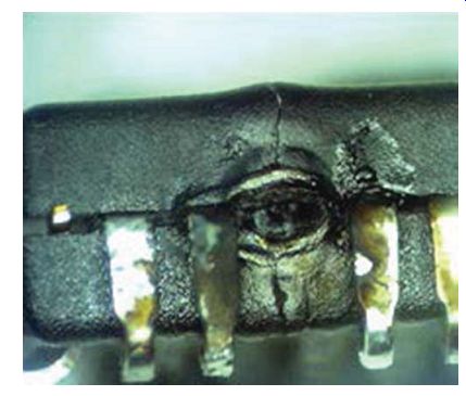
FIG. 8 EOS failure mechanism--packaging
FIG. 8 is an example of package pin damage due to EOS. From the package damage and package pin, it is clear that the region underwent significant currents leading to failure.
There are also failure types associated with long time constant pulses. Phenomena affiliated with long pulse width significantly longer than the thermal diffusion time constant of the structure are prone to thermal transport, heating, and electromigration.
Hence, processes that involve material transport, thermal stress, and mechanical stress are more affiliated with EOS. The resulting packaging ablation is associated with both thermal and mechanical stress [1].
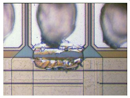
FIG. 9 EOS failure mechanism--bond pads
EOS events can shorten the reliability lifetime of components, leading to an early wearout and inducing shifts in the reliability "bathtub" curve of a component. As discussed in the previous sections, this will be a bigger issue as advanced components are scaled.
Where it is hard to distinguish between EOS and ESD is in the failure signature of a component. Both EOS and ESD can introduce "on-chip" failure mechanisms whose visual failure signatures are similar. Both EOS and ESD can create the following failures:
• Dielectric breakdown
• Interlevel dielectric cracking
• Metal failures
• Molten semiconductor damage.
At times, failure analysts distinguish these events based on physical size. Typically, EOS events create a larger failure damage, more distributed through the semiconductor chip; but this is dependent on the ESD event type. FIG. 9 is EOS of the wire interconnects bond pad.
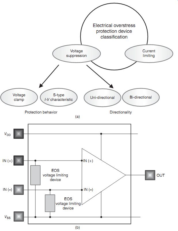
FIG. 10 (a) Electrical overvoltage (EOV) protection classification.
(b) Electrical overvoltage (EOV) protection network
9. Electrical Overstress (EOS) Protection Circuit Solutions
Today, EOS is still an issue in today's electronic systems [6-10]. To address EOS in systems, EOS protection devices are added to PCB, cards, and systems. In this section, the focus will be on providing an understanding of the different classifications and types of EOS protection devices used today. EOS protection devices are supported by a large variety of technologies. Although material and operation may differ between the EOS protection devices, their electrical characteristics can be classified into a few fundamental groups. EOS protection networks can be identified as a voltage suppression device or as a current-limiting device. The voltage suppression device limits the voltage observed on the signal pins or power rails of a component, preventing EOV. The current-limiting device prevents a high current from reaching sensitive nodes, avoiding EOC.
Voltage suppression devices can also be subdivided into two major classifications.
FIG. 10(a) illustrates examples of voltage suppression categories. Voltage suppression devices can be segmented into devices that remain with a positive differential resistance and those that undergo a negative resistance region. For positive differential resistance, these devices can be referred to as "voltage clamp" devices where dI/dV remains positive for all states; for the second group, there exists a region where dI/dV is negative. The first group can be classified as "voltage clamp devices," whereas the second group can be referred to as an "S-type I-V characteristic device," or as a "snapback device." In the classification of voltage suppression devices, the second classification can be associated with the directionality; a voltage suppression device can be "unidirectional" or "bidirectional." FIG. 10(b) illustrates an example of an EOV device solution integrated with a differential circuit.
To prevent EOS associated with EOV, voltage suppression devices are mounted on PCB, or integrated into systems. The choice of EOS device to use in an application is dependent on the electrical characteristics, cost, and size. The electrical characteristics that are of interest are the breakdown voltage and the forward conduction.
Types of voltage suppression devices used EOS are as follows:
• Transient voltage suppression (TVS) diodes
• Thyristor devices
• Varistor devices
• Polymer voltage suppression (PVS) devices
• Gas discharge tube (GDT) devices.
Current-limiting devices can be used in a series configuration for EOS protection. EOS current-limiting devices can be as follows:
• Resistors
• Resetting fuses
• Non-resetting fuses
• eFUSE
• Positive temperature coefficient (PTC) devices
• Circuit breakers.
The choice of the current-limiting EOS protection device is a function of the cost, size, rated current, time response, I 2t value, rated voltage, voltage drops, and application requirements.
FIG. 11 illustrates an example of an EOC protection device solution integrated with a differential circuit. For EOC solutions, series resistor elements or other networks are suitable to limit the current lowing into the inputs of sensitive circuitry.
Diodes are a commonly used unidirectional EOS protection device. Diodes provide a for ward conduction state and reverse blocking state. For EOS single component, diodes are mounted on PCB by soldering in the leads through vias or surface mount. Diodes are commonly used within components to provide ESD protection for internal circuitry [1].
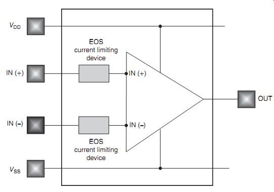
FIG. 11 Electrical overcurrent (EOC) protection
Electrical characteristics of a diode structure include forward turn-on, the on-resistance, and reverse breakdown voltage. At high current conditions, in the forward conduction state, thermal breakdown occurs as well as thermal failure of the diode structure. If the EOS stress current exceeds the thermal breakdown of the diode structure, destructive failure of the element can lead to system degradation or an EOS failure.
Diodes are unidirectional type EOS structure but can be utilized in a forward or reverse breakdown mode of operation for a voltage-limiting EOS solution [6]. The power-to-failure of a diode structure is higher in the forward-mode of operation compared to its reverse breakdown mode of operation. In a forward conduction mode, the power distributes through all sections of the element (e.g., anode, cathode, and metallurgical junction). In the reverse conduction mode, power is contained only in the metallurgical junction region.
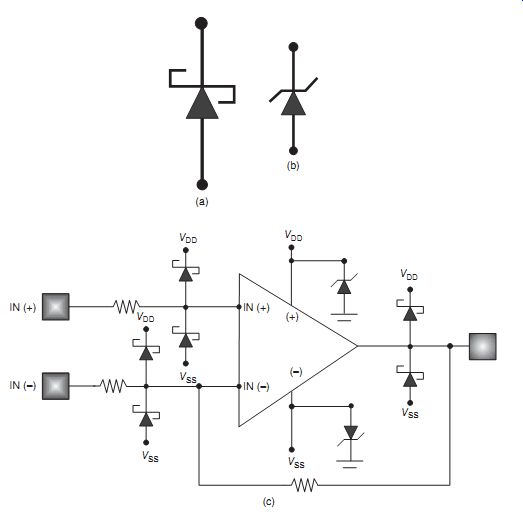
FIG. 12 (a) EOS protection--Schottky diode. (b) EOS protection--Zener
diode. (c) EOS protection--operational amplifier with Schottky and Zener
protection
Schottky diodes are a commonly used EOS protection device (FIG. 12). Schottky diodes have a forward conduction state and reverse blocking state. Schottky diodes have a lower forward turn-on (e.g., 0.35V) compared to standard silicon p-n junction (e.g., 0.7V).
For EOS single component, Schottky diodes are mounted on PCB by soldering in the leads through vias or surface mount. Schottky diodes are not commonly used within components to provide ESD protection due to lack of availability. Schottky diodes are unidirectional type EOS structure but can be utilized in a forward or reverse breakdown mode of operation for a voltage-limiting EOS solution.
Zener diodes are used as a unidirectional EOS protection device [1]. Zener diodes are typically used as a voltage clamping EOS protection device, and typically used in the breakdown state. Zener diodes have a well-defined voltage breakdown value.
Zener diodes are used for ESD protection for high voltage and power applications. Zener diodes are not used for ESD protection for low-voltage complementary metal-oxide semiconductor (CMOS) applications. For EOS single component, Zener diodes are mounted on PCB by soldering in the leads through vias or surface mount.
Zener diodes are unidirectional type EOS structure but can be utilized primarily in reverse breakdown mode of operation for a voltage-limiting EOS solution.
Zener diodes are used as a unidirectional EOS protection device. Zener diodes are typically used as a voltage clamping EOS protection device and typically used in the breakdown state. Zener diodes have a well-defined voltage breakdown value. Figure 8.11 is the symbol for the Zener diode.
Schottky and Zener diodes can be integrated into a given application. FIG. 12(c) shows an example of an EOS protection scheme that utilizes both Schottky and Zener diode elements.
An EOS protection device used for high voltages is varistor. A varistor is also known as a voltage-dependent resistor (VDR). A varistor is a portmanteau--combining the word for variable and resistor. In reality, the varistor element behaves like a diode, forming a nonlinear current-voltage (I-V characteristic). The element has the characteristics of being bidirectional voltage clamp (note: it does not form an S-type I-V characteristic or undergo a negative resistance regime). At low voltages, the device has a high series resistance, serving as an "off-state." At higher voltages, the device "turns-on" and has a low resistance.
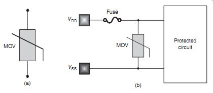
FIG. 13 (a) EOS protection--metal oxide varistor (MOV). (b) EOS protection--metal
oxide varistor (MOV) for power supply
The metal oxide varistor (MOV) device is the most common varistor composition.
FIG. 13(a) is the circuit schematic symbol for an MOV device. Zinc oxide, combined with other metal oxides, is integrated between two metal electrodes. Other metal oxides integrated include bismuth, cobalt, and manganese. The operation of the MOV device is based on conduction through ZnO grains; current lows "diode-like" through the grain structures creating a low current low at low voltages. At higher voltages, the current low is dominated by a combination of thermionic emissions and tunneling. This behavior forms a diode-like I-V characteristic providing the high-resistance/low-voltage state, and the low-resistance/high-voltage state. From the I-V characteristic, a "clamping voltage" can be defined (e.g., analogous to a diode turn-on voltage). The characteristic that influences the on-resistance and the turn-on voltage is a function of the ZnO grain structure, the film thickness, the physical size, and the other metal oxides integrated into the structure.
The advantage of the MOV structure is it has a high trigger voltage, making it suitable for EOS protection in power electronics (e.g., 120-700V applications). The disadvantage of these elements is that it has high capacitance and high on-resistance. A second disadvantage is that the high trigger voltage does not make it suitable for advanced high-speed or low-voltage electronics. A third disadvantage is the variability of the device response (e.g., on resistance and clamping voltage) in the MOV device characteristics. Key device parameters of varistor are the energy rating, operating voltage, response time, maximum current, and breakdown voltages.
FIG. 13(b) is an example of usage of an MOV for power supply protection. The MOV element can be placed between the power supply and ground to avoid EOS to the VDD power supply.
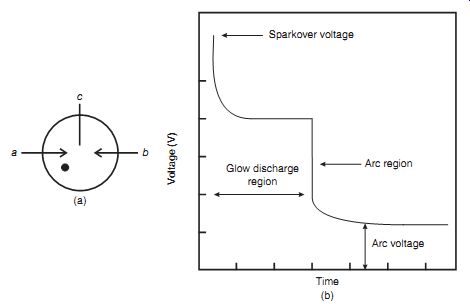
FIG. 14 (a) EOS protection--gas discharge tube (GDT). (b) EOS protection--gas
discharge tube (GDT) I-t plot
GDT devices can be used to avoid EOS in systems (FIG. 14(a)) [1]. GDT are bidirectional, allowing for protection of both positive and negative EOS events. GDT elements are suitable for surge protection, high-voltage electronic "crowbars," to lightning. GDT devices are not suitable for EOS protection of low-voltage electronics due to the high trigger voltages (unless used as a first stage followed by other low-voltage secondary EOS solutions).
GDT utilize electrical discharge in gases. An applied voltage initiates the device by ionizing the electrical gas, followed by electrical glow discharge and an electrical arc. With creation of an electrical arc, the GDT device becomes a low-resistance shunt for EOS protection. These gas-filled tubes can contain hydrogen, deuterium, and noble gases (e.g., helium, neon, argon, krypton, and xenon). GDT devices can vary their electrical characteristics by choices of the gas type, pressure, electrode design, and spacings.
FIG. 14(b) shows an example of a ramp impulse voltage versus time for a GDT device.
GDT devices undergo three states: (1) electrical breakdown, (2) glow discharge, and (3) electrical arc. The electrical breakdown is a high-voltage, low-current state prior to triggering of the GDT device. A glow discharge region forms a second state that incorporates a low-current, high-voltage state. Lastly, after full ionization of the gas, a low-voltage, high-current state occurs with a low "on-resistance." GDT devices have high trigger voltages suitable for LDMOS power electronic applications to HV LDMOS (e.g., 120V), and UHV LDMOS applications (e.g., 600-700V). These devices are used in a number of high-voltage switch devices, such as ignitrons, krytrons, and thyratrons. One of the disadvantages of the GDT devices is the slow turn-on times typically in the microseconds. An example of some of the electrical characteristics can exhibit DC breakdown from 75 to 600V, with a single surge response of 40 kA in 10-20 µs, or multiple surges of magnitude of 20 kA.
In time, when a voltage disturbance reaches the GDT sparkover voltage, the GDT will switch into a low impedance state, also known as the "arc mode." With this low resistance state, the GDT device will discharge the EOS event to the ground, avoiding EOS failure of the component.
At voltages below the sparkover voltage, the GDT remains in a high impedance off-state.
As the voltage increases, the GDT enters the "glow voltage region"; this glow region is where ionization starts to occur within the GDT. As the current increases, avalanche multiplication occurs, leading to further ionization of the gas within the GDT. This is followed by avalanche breakdown and the low impedance state. The voltage condition developed across the GDT during this state is called the "arc voltage." The transition time between the glow and arc regions is dependent on the impulse current, electrode shape (e.g., electrode curvature), electrode spacing, gas composition, gas pressure, and emission coatings.
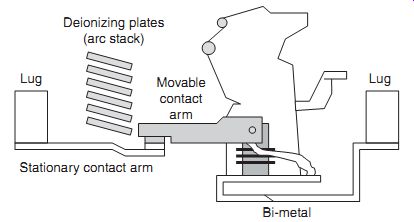
FIG. 15 EOS protection--thermal circuit breakers
For EOC, the electrical circuit breaker is used in industrial, commercial, and residential electrical systems. Electrical circuit breakers are typically not found in semiconductor chips, or small systems due to the physical size, weight, cost, and time response. Circuit breakers can be used to protect household appliances and large-scale switchgear high-voltage circuits.
The circuit breaker is an electrical switch designed for the purpose of EOC events, short circuits, or fault detection. Circuit breakers are typically "tripped" by the high current event and can be manually reset. The concept of the circuit breaker was invented by Charles Grafton Page in 1836 [1]. A pilot device senses a fault current and operates a trip opening mechanism.
The trip solenoid releases a latch. Some high-voltage circuit breakers are self-contained with current transformers, protection relays, and an internal control power source. With detection of an electrical fault, the circuit breaker contacts open to interrupt the circuit; some mechanically stored energy contained within the breaker is used to separate the contacts. The circuit breaker can be reset manually after the event is over. Circuit breakers are nondestructive, as opposed to fuses that may only have a single use (FIG. 15). Nowadays, both fuses and circuit breakers can be integrated into a common system.
A class of circuit breakers is the thermal-magnetic circuit breaker. Thermal-magnetic circuit breakers are used to avoid "short-circuit" currents. Thermal-magnetic circuit breakers are sensitive to temperature.
FIG. 15 shows an example of a thermal-magnetic circuit breaker. Thermal-magnetic circuit breakers contain a bimetal switch and an electromagnet. The bimetal switch provides overcurrent protection. During current overload, the bimetal switch heats up, leading to bending of the element.
The electromagnet responds to short-circuit currents. The electromagnetic is a wire coil and an iron core. As a high current goes through the coil, induced magnetic field attracts an armature of the thermal-magnetic circuit breaker. When the armature extends toward the electromagnet due to the magnetic force, the armature rotates the trip bar. With the tripping of the trip bar, the current path is "open," and circuit breaker prevents the EOC.
Power controllers are used for low-power and low-voltage applications [1]. Power controllers are typically low-voltage, high-efficiency products that can carry amperes of current per channel. Buck-converters contain overcurrent protection logic and networks; overcurrent functions protect the switching converter from an output short by monitoring current low in the application. Overcurrent fault counters prevent turn-on of circuitry until the fault has passed, and the system is on its next switching cycle. Flags are triggered in the counters after the overcurrent fault condition (OFC). When the overcurrent condition lag is reset, the circuitry is allowed to reinitiate. This "soft start" eliminates the inrush current during the start and restart.
FIG. 16 shows the integration of the fault, soft start, and control logic at the outputs of the overcurrent and overvoltage comparators. The soft start function outputs a ramp reference for both the voltage and current loops.
Hence, in power applications, it is possible to integrate EOV and EOC within a component design. Many analog and power applications also contain thermal protection networks to avoid thermal runaway and EOS damage.
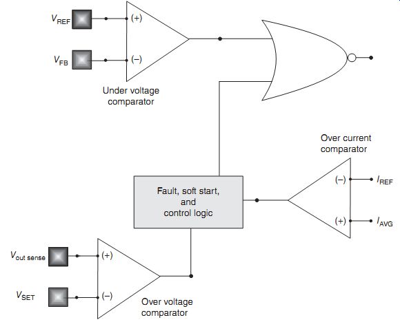
FIG. 16 EOS protection--soft start EOC and EOV protection circuitry
10. Electrical Overstress (EOS) Testing--TLP Method and EOS
Transmission line pulse (TLP) testing methodology can be utilized to quantify EOS robustness in both components and systems. Today's TLP methodology is a "two-pin" test to determine the TLP I-V characteristic. TLP measurements can provide information of the characteristics of a single device or a signal pin. TLP measurements can provide the following current and voltage metrics:
• Trigger voltage (Vt1)
• Holding voltage (Vh)
• Sustaining voltage (Vsus)
• On-resistance (Ron)
• Second trigger voltage (Vt2)
• Second breakdown current (It2).
TLP testing is used till today for device characterization and qualification of components in a technology. The choice of the TLP pulse width was chosen for equivalency for the HBM energy (e.g., integrated energy of the applied pulse). For EOS, this methodology can be extended to longer pulse width for evaluation of long pulse events.
10.1 Electrical Overstress (EOS) Testing--Long Duration Transmission Line Pulse (LD-TLP) Method
The methodology of TLP testing can be utilized for components and systems for EOS. For evaluation of EOS, the TLP methodology can be modified as follows:
• Long pulse
• Variable pulse width
• Component ground reference
• PCB ground reference.
10.2 Electrical Overstress (EOS) Testing--Transmission Line Pulse (TLP) Method, EOS, and the Wunsch-Bell Model
Modification of the present TLP methodology where the pulse width is varied from short pulses to long pulse events, the power-to-failure as a function of the pulse event can be quantified.
By establishing a power-to-failure versus pulse width plot, a "universal curve" is formed that fully characterizes the device under test for all pulse lengths. Historically, this was established methodology for evaluation of the power-to-failure for wide bandwidth pulse events (e.g., electromagnetic pulse, EMP). The power-to-failure versus pulse width plot is known as the Wunsch-Bell plot, as discussed in the previous sections. With the evaluation of the Wunsch-Bell curve, the full spectrum from short pulse to long pulse events can be understood (FIGs 17 and 18).
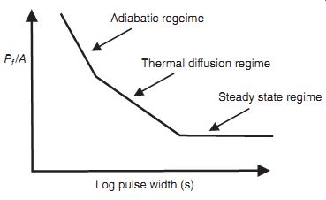
FIG. 17 Wunsch-Bell power to failure plot
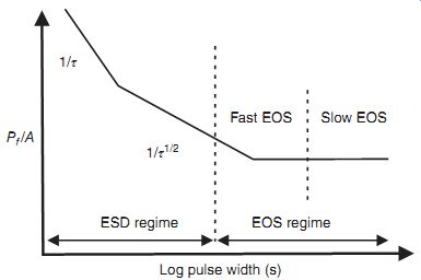
FIG. 18 Slow and fast EOS domain in the Wunsch-Bell curve
10.3 Electrical Overstress (EOS) Testing--Limitations of the Transmission Line Pulse (TLP) Method for the Evaluation of EOS for Systems
For evaluations of components and systems, there are some limitations to the TLP method.
A first issue is that in a system environment, an EOS event can propagate through multiple current paths. TLP analysis of components is successful when applying a single device or a single signal pin. In a full component or a system, the TLP current can low through different current paths. A second issue is the bridging between the single device and full system level response. Due to the nonlinear nature of the semiconductor devices, the superposition of currents is not always valid in bridging from the single device TLP I-V characteristic to the full component or system level.
10.4 Electrical Overstress (EOS) Testing--Electromagnetic Pulse (EMP)
A source of an EOS event is the EMP event. The EMP event is defined as a high amplitude, single pulse, short duration, and broadband pulse of electromagnetic energy. EMP is the electromagnetic effect resulting from the detonation of a nuclear device. Other definitions of EMP at high altitudes are high-altitude electromagnetic pulse (HEMP), HAEMP, and HNEMP.
EMP test methods include MIL-STD-461; this provides radiated (RS 105) and conducted (CS 116) test methods and test levels for determining a device's immunity to EMP. The RS 105 radiated test methodology addresses the risk of radiated exposure to an EMP event; this test is applicable to equipment installed in exposed and partially exposed environments on aircraft, surface ships, submarines, and ground vehicles. The CS116 coupling test method addresses the effects of EMP coupling onto interconnecting wiring harnesses; this test is to ensure the equipment's immunity to damped sinusoidal transients induced on the equipment's cables. Testing is generally applicable to all applications with limited applicability to submarine equipment.
The MIL-STD-188-125 establishes minimum requirements and design objectives for HEMP hardening of fixed, ground-based facilities that perform critical, time-urgent command, control, communications, computer, and intelligence (C4I) missions. Similar to the approach described in MIL-STD-461, this standard provides both radiated and conducted test methods and test levels.
11. Electrical Overstress (EOS) Testing--DC and Transient Latchup Testing
CMOS latchup can occur from EOS when regenerative feedback occurs within a semiconductor chip circuitry. From 1979 to 2000, CMOS latchup occurred within a given circuit.
Due to scaling of technologies, CMOS latchup occurred between the following:
• I/O PFET to I/O NFET
• I/O to ESD protection circuit
• I/O to ESD power clamp circuit
• I/O to I/O
• I/O to adjacent circuit element (e.g., decoupling capacitors)
• I/O to core circuitry
• Core to core circuitry.
CMOS latchup is evaluated in both the DC and transient state. The integrated circuit latchup standard most commonly used is the JEDEC JESD 78:2010 standard for integrated circuit latchup test, as discussed in Section 11. Many of the EOS pulse-defined events should be used to determine if CMOS latchup can occur. For example, cable discharge events (CDE) can lead to CMOS latchup. In addition, latchup is typically evaluated on a component level.
A semiconductor component can survive the JESD78 latchup IC specification but fail on a PCB or card. Latchup testing should be evaluated on both the semiconductor chip level and the populated PCB and system level to avoid card failures due to CMOS latchup.
12. Summary and Closing Comments
This section looked at the broader issue of EOS. The topic of EOS was approached providing distinctions of EOS versus ESD phenomena, and EOS versus CMOS latchup. The section discussed specific EOS tests that are presently used for systems and for semiconductor chips, as well as growing interest in "long pulse transmission line pulse (TLP)" testing method that is having increased popularity to address EOS phenomena. EOS failure mechanisms and solutions were quantified. With the growing increase of system level issues, EOS has been seeing a renewed interest for both semiconductor chip developers and system designers.
Section 13 addresses electromagnetic compatibility (EMC). In this section, scanning methods for evaluation of EMC sensitivity are discussed. New state-of-the-art EMC scanning techniques are the highlights of the section.
Problems
1. How can we quantify EOS robustness when the variety of EOS events are significant?
2. For EOS robustness qualification, it is possible to have a set of different criteria and tests that are required to pass in order to qualify a component. Define a set of tests that can be performed in order to pass "EOS robustness qualification."
3. On a Wunsch-Bell plot, highlight the regions that are regarded as the regime where EOS events occur.
4. Using a Wunsch-Bell plot, define a set of tests that can be performed to cover quantification of the EOS robustness of a test structure or component.
5. Long pulse transmission line pulse (LP-TLP) is a test to cover the time regime of EOS events. What are the advantages? What are potential problems?
6. EOS events can be defined as a "slow EOS" regime. How do these regimes correspond to the Wunsch-Bell model (e.g., adiabatic, thermal diffusion, and steady state regimes)?
7. EOS events can be defined as "slow EOS" regime and "fast EOS regime." How do these regimes correspond to the Dwyer-Cambell-Franklin model?
8. EOS can include electromagnetic pulse (EMP) events. How does one quantify robustness from an EMP event? What is the frequency that one evaluates for EMP?
References
[not listed]