AMAZON multi-meters discounts AMAZON oscilloscope discounts
OVERVIEW
The speed of light is just too slow. Commonplace, modern, volume-manufactured digital designs require control of timings down to the picosecond range. The amount of time it takes light from your nose to reach your eye is about 100 picoseconds (in 100 ps, light travels about 1.2 in.). This level of timing must not only be maintained at the silicon level, but also at the physically much larger level of the system board, such as a computer motherboard.
These systems operate at high frequencies at which conductors no longer behave as simple wires, but instead exhibit high-frequency effects and behave as transmission lines that are used to transmit or receive electrical signals to or from neighboring components. If these transmission lines are not handled properly, they can unintentionally ruin system timing.
Digital design has acquired the complexity of the analog world and more. However, it has not always been this way. Digital technology is a remarkable story of technological evolution. It’s a continuing story of paradigm shifts, industrial revolution, and rapid change that is unparalleled. Indeed, it’s a common creed in marketing departments of technology companies that "by the time a market survey tells you the public wants something, it’s already too late." This rapid progress has created a roadblock to technological progress that this guide will help solve. The problem is that modern digital designs require knowledge that has formerly not been needed. Because of this, many currently employed digital system designers don’t have the knowledge required for modern high-speed designs. This fact leads to a surprisingly large amount of misinformation to propagate through engineering circles. Often, the concepts of high-speed design are perceived with a sort of mysticism. However, this problem has not come about because the required knowledge is unapproachable. In fact, many of the same concepts have been used for several decades in other disciplines of electrical engineering, such as radio-frequency design and microwave design. The problem is that most references on the necessary subjects are either too abstract to be immediately applicable to the digital designer, or they are too practical in nature to contain enough theory to fully understand the subject. This guide will focus directly on the area of digital design and will explain the necessary concepts to understand and solve contemporary and future problems in a manner directly applicable by practicing engineers and/or students. It’s worth noting that everything in this guide has been applied to a successful modern design.
__1. THE BASICS
As the reader undoubtedly knows, the basic idea in digital design is to communicate information with signals representing 1s or 0s. Typically this involves sending and receiving a series of trapezoidal shaped voltage signals such as shown in FIG. 1 in which a high voltage is a 1 and a low voltage is a 0. The conductive paths carrying the digital signals are known as interconnects. The interconnect includes the entire electrical pathway from the chip sending a signal to the chip receiving the signal. This includes the chip packages, connectors, sockets, as well as a myriad of additional structures. A group of interconnects is referred to as a bus. The region of voltage where a digital receiver distinguishes between a high and a low voltage is known as the threshold region. Within this region, the receiver will either switch high or switch low. On the silicon, the actual switching voltages vary with temperature, supply voltage, silicon process, and other variables. From the system designers point of view, there are usually high-and low-voltage thresholds, known as Vih and Vil, associated with the receiving silicon, above which and below which a high or low value can be guaranteed to be received under all conditions. Thus the designer must guarantee that the system can, under all conditions, deliver high voltages that do not, even briefly, fall below Vih, and low voltages that remain below Vil, in order to ensure the integrity of the data.
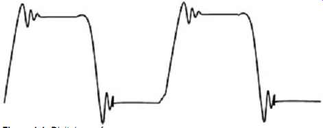
FIG. 1: Digital waveform.
In order to maximize the speed of operation of a digital system, the timing uncertainty of a transition through the threshold region must be minimized. This means that the rise or fall time of the digital signal must be as fast as possible. Ideally, an infinitely fast edge rate would be used, although there are many practical problems that prevent this. Realistically, edge rates of a few hundred picoseconds can be encountered. The reader can verify with Fourier analysis that the quicker the edge rate, the higher the frequencies that will be found in the spectrum of the signal. Herein lies a clue to the difficulty. Every conductor has a capacitance, inductance, and frequency-dependent resistance. At a high enough frequency, none of these things is negligible. Thus a wire is no longer a wire but a distributed parasitic element that will have delay and a transient impedance profile that can cause distortions and glitches to manifest themselves on the waveform propagating from the driving chip to the receiving chip. The wire is now an element that is coupled to everything around it, including power and ground structures and other traces. The signal is not contained entirely in the conductor itself but is a combination of all the local electric and magnetic fields around the conductor. The signals on one interconnect will affect and be affected by the signals on another. Furthermore, at high frequencies, complex interactions occur between the different parts of the same interconnect, such as the packages, connectors, vias, and bends. All these high-speed effects tend to produce strange, distorted waveforms that will indeed give the designer a completely different view of high-speed logic signals. The physical and electrical attributes of every structure in the vicinity of the interconnect has a vital role in the simple task of guaranteeing proper signaling transitions through Vih and Vil with the appropriate timings. These things also determine how much energy the system will radiate into space, which will lead to determining whether the system complies with governmental emission requirements. We will see in later Sections how to account for all these things.
When a conductor must be considered as a distributed series of inductors and capacitors, it’s known as a transmission line. In general, this must be done when the physical size of the circuit under consideration approaches the wavelength of the highest frequency of interest in the signal. In the digital realm, since edge rate pretty much determines the maximum frequency content, one can compare rise and fall times to the size of the circuit instead, as shown in FIG. 2. On a typical circuit board, a signal travels about half the speed of light (exact formulas will be in later Sections). Thus a 500 ps edge rate occupies about 3 in. in length on a circuit trace. Generally, any circuit length at least 1/10th of the edge rate must be considered as a transmission line.
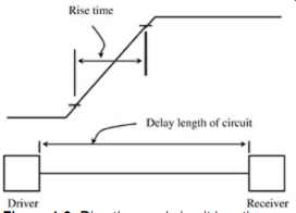
FIG. 2: Rise time and circuit length.
One of the most difficult aspects of high-speed design is the fact that there are a large number codependent variables that affect the outcome of a digital design. Some of the variables are controllable and some force the designer to live with the random variation. One of the difficulties in high-speed design is how to handle the many variables, whether they are controllable or uncontrollable. Often simplifications can be made by neglecting or assuming values for variables, but this can lead to unknown failures down the road that will be impossible to "root cause" after the fact. As timing becomes more constrained, the simplifications of the past are rapidly dwindling in utility to the modern designer. This guide will also show how to incorporate a large number of variables that would otherwise make the problem intractable. Without a methodology for handling the large amount of variables, a design ultimately resorts to guesswork no matter how much the designer physically understands the system. The final step of handling all the variables is often the most difficult part and the one most readily ignored by a designer. A designer crippled by an inability to handle large amounts of variables will ultimately resort to proving a few "point solutions" instead and hope that they plausibly represent all known conditions. While sometimes such methods are unavoidable, this can be a dangerous guessing game. Of course, a certain amount of guesswork is always present in a design, but the goal of the system designer should be to minimize uncertainty.
__2. THE PAST AND THE FUTURE
Gordon Moore, co-founder of Intel Corporation, predicted that the performance of computers will double every 18 months. History confirmed this insightful prediction. Remarkably, computer performance has doubled approximately every 1.5 years, along with substantial decreases in their price. One measure of relative processor performance is internal clock rates. FIG. 3 shows several processors through history and their associated internal clock rates. By the time this is in print, even the fastest processors on this chart will likely be considered unimpressive. The point is that computer speeds are increasing exponentially.
As core frequency increases, faster data rates will be demanded from the buses that feed information to the processor, as shown in FIG. 4, leading to an interconnect timing budget that is decreasing exponentially. Decreased timing budgets mean that it’s evermore important to properly account for any phenomenon that may increase the timing uncertainty of the digital waveform as it arrives at the receiver. This is the root cause of two inescapable obstacles that will continue to make digital system design difficult. The first obstacle is simply that the sheer amount of variables that must be accounted for in a digital design is increasing. As frequencies increase, new effects, which may have been negligible at slower speeds, start to become significant. Generally speaking, the complexity of a design increases exponentially with increasing variable count. The second obstacle is that the new effects, which could be ignored in designs of the past, must be modeled to a very high precision. Often these new models are required to be three-dimensional in nature, or require specialized analog techniques that fall outside the realms of the digital designer's discipline.
The obstacles are perhaps more profound on the subsystems surrounding the processor since they evolve at a much slower rate, but still must support the increasing demands of the processor.
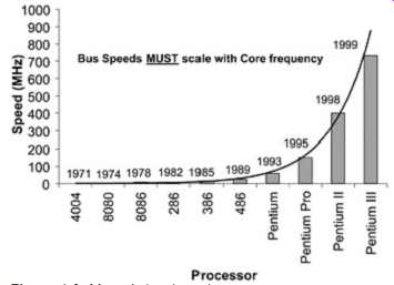
FIG. 3: Moore's law in action.
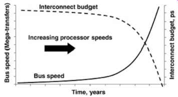
FIG. 4: The interconnect budget shrinks as the performance and frequency
of the system increases.
All of this leads to the present situation: There are new problems to solve. Engineers who can solve these problems will define the future. This guide will equip the reader with the necessary practical understanding to contend with modern high-speed digital design and with enough theory to see beyond this guide and solve problems that the authors have not yet encountered. Read on.