AMAZON multi-meters discounts AMAZON oscilloscope discounts
In today's high-speed digital systems, it’s necessary to treat the printed circuit board (PCB) or multichip module (MCM) traces as transmission lines. It’s no longer possible to model interconnects as lumped capacitors or simple delay lines, as could be done on slower designs. This is because the timing issues associated with the transmission lines are becoming a significant percentage of the total timing margin. Great attention must be given to the construction of the PCB so that the electrical characteristics of the transmission lines are controlled and predictable. In this Section we introduce the basic transmission line structures typically used in digital systems and present basic transmission line theory for the ideal case. The material presented in this Section provides the necessary knowledge base needed to comprehend all subsequent Sections.
1. TRANSMISSION LINE STRUCTURES ON A PCB OR MCM
Transmission line structures seen on a typical PCB or MCM consist of conductive traces buried in or attached to a dielectric or insulating material with one or more reference planes.
The metal in a typical PCB is usually copper and the dielectric is FR4, which is a type of fiberglass. The two most common types of transmission lines used in digital designs are microstrips and striplines. A microstrip is typically routed on an outside layer of the PCB and has only one reference plane. There are two types of microstrips, buried and non-buried. A buried (sometimes called embedded) microstrip is simply a transmission line that is embedded into the dielectric but still has only one reference plane. A stripline is routed on an inside layer and has two reference planes. FIG. 1 represents a PCB with traces routed between the various components on both internal (stripline) and external (microstrip) layers.
The accompanying cross section is taken at the given mark so that the position of transmission lines relative to the ground/power planes can be seen. In this guide, transmission lines are often represented in the form of a cross section. This is very useful for calculating and visualizing the various transmission line parameters described later.
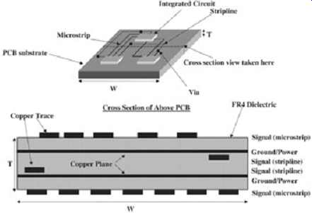
FIG. 1: Example transmission lines in a typical design built on a PCB.
Multiple-layer PCBs such as the one depicted in FIG. 1 can provide a variety of stripline and microstrip structures. Control of the conductor and dielectric layers (which is referred to as the stackup) is required to make the electrical characteristics of the transmission line predictable. In high-speed systems, control of the electrical characteristics of the transmission lines is crucial. These basic electrical characteristics, defined in this Section, will be referred to as transmission line parameters.
2. WAVE PROPAGATION
At high frequencies, when the edge rate (rise and fall times) of the digital signal is small compared to the propagation delay of an electrical signal traveling down the PCB trace, the signal will be greatly affected by transmission line effects. The electrical signal will travel down the transmission line in the way that water travels through a long square pipe. This is known as electrical wave propagation. Just as the waterfront will travel as a wave down the pipe, an electrical signal will travel as a wave down a transmission line. Additionally, just as the water will travel the length of the pipe in a finite amount of time, the electrical signal will travel the length of the transmission line in a finite amount of time. To take this simple analogy one step further, the voltage on a transmission line can be compared to the height of the water in the pipe, and the flow of the water can be compared to the current. FIG. 2 depicts a common way of representing a transmission line. The top line is the signal path and the bottom line is the current return path. The voltage Vi is the initial voltage launched onto the line at node A, and Vs and Zs form a Thévenin equivalent representation of the output buffer, usually referred to as the source or the driver.
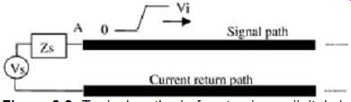
FIG. 2: Typical method of portraying a digital signal propagating on a
transmission line.
3. TRANSMISSION LINE PARAMETERS
To analyze the effects that transmission lines have on high-speed digital systems, the electrical characteristics of the line must be defined. The basic electrical characteristics that define a transmission line are its characteristic impedance and its propagation velocity. The characteristic impedance is similar to the width of the water pipe used in the analogy above, and the propagation velocity is simply analogous to speed at which the water flows through the pipe. To define and derive these terms, it’s necessary to examine the fundamental properties of a transmission line. As a signal travels down the transmission line depicted in FIG. 2, there will be a voltage differential between the signal path and the current return path (generically referred to as a ground return path or an ac ground even when the reference plane is a power plane). When the signal reaches an arbitrary point z on the transmission line, the signal path conductor will be at a potential of Vi volts and the ground return conductor will be at a potential of 0 V. This voltage difference establishes an electric field between the signal and the ground return conductors. Furthermore, Ampère's law states that the line integral of the magnetic field taken about any given closed path must be equal to the current enclosed by that path. In simpler terms, this means that if a current is flowing through a conductor, it results in a magnetic field around that conductor. We have therefore established that if an output buffer injects a signal of voltage Vi and current Ii onto a transmission line, it will induce an electric and a magnetic field, respectively. However, it should be clear that the voltage Vi and current Ii , at any arbitrary point on the line z will be zero until the time z/v, where v is the velocity of the signal traveling down the transmission line and z is the distance from the source. Note that this analysis implies that the signal is not simply traveling on the signal conductor of the transmission line; rather, it’s traveling between the signal conductor and reference plane in the form of an electric and a magnetic field.
Now that the basic electromagnetic properties of a transmission line have been established, it’s possible to construct a simple circuit model for a section of the line. FIG. 3 represents a cross section of a microstrip transmission line and the electric and magnetic field patterns associated with a current flowing though the line. If it’s assumed that there are no components of the electric or magnetic fields propagating in the z-direction (into the page), the electric and magnetic fields will be orthogonal. This is known as transverse electro-magnetic mode (TEM). Transmission lines will propagate in TEM mode under normal circumstances and it’s an adequate approximation even at relatively high frequencies. This allows us to examine the transmission line in differential sections (or slices) along the length of the line traveling in the z-direction (into the page). The two components shown in FIG. 3 are the electric and magnetic fields for an infinitesimal or differential section (slice) of the transmission line of length dz. Since there is energy stored in both an electric and a magnetic field, let us include the circuit components associated with this energy storage in our circuit model. The magnetic field for a differential section of the transmission line can be represented by a series inductance Ldz, where L is inductance per length. The electric field between the signal path and the ground path for a length of dz can be represented by a shunt capacitor C dz, where C is capacitance per length. An ideal model would consist of an infinite number of these small sections cascaded in series. This model adequately describes a section of a loss-free transmission line (i.e., a transmission line with no resistive losses).
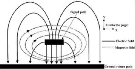
FIG. 3: Cross section of a microstrip depicting the electric and magnetic
fields assuming that an electrical signal is propagating down the line
into the page.
However, since the metal used in PCB boards is not infinitely conductive and the dielectrics are not infinitely resistive, loss mechanisms must be added to the model in the form of a series resistor, R dz, and a shunt resistor to ground referred to as a conductance, G dz, with units of siemens (1/ohm). FIG. 4 depicts the equivalent circuit model for a differential section of a transmission line. The series resistor, R dz, represents the losses due to the finite conductivity of the conductor; the shunt resistor, G dz, represents the losses due to the finite resistance of the dielectric separating the conductor and the ground plane, the series inductor, Ldz, represents the magnetic field; and the capacitor, C dz, represents the electric field between the conductor and the ground plane. In the remainder of this guide, one of these sections will be known as an RLCG element.
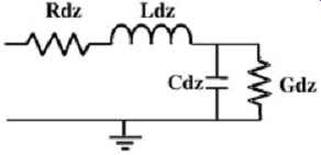
FIG. 4: Equivalent circuit model of a differential section of a transmission
line of length dz (RLCG model).
3.1. Characteristic Impedance
The characteristic impedance Zo of the transmission line is defined by the ratio of the voltage and current waves at any point of the line; thus, V/I = Zo. FIG. 5 depicts two representations of a transmission line. FIG. 5a represents a differential section of a transmission line of length dz modeled with an RLCG element as described above and terminated in an impedance of Zo. The characteristic impedance of the RLCG element is defined as the ratio of the voltage V and current I, as depicted in FIG. 5a. Assuming that the load Zo is exactly equal to the characteristic impedance of the RLCG element, FIG. 5a can be represented by FIG. 5b, which is an infinitely long transmission line. The termination, Zo, in FIG. 5a simply represents the infinite number of additional RLCG segments of impedance Zo that comprise the complete transmission line model. Since the voltage/current ratio in the terminating device, Zo, will be the same as that in the RLCG segment, then from the perspective of the voltage source, FIG. 5a and b will be indistinguishable. With this simplification, the characteristic impedance can be derived for an infinitely long transmission line.
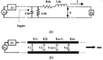
FIG. 5: Method of deriving a transmission lines characteristic impedance:
(a) differential section; (b) infinitely long transmission line.
To derive the characteristic impedance of the line, FIG. 5a should be examined. Solving the equivalent circuit of FIG. 5a for the input impedance with the assumption that the characteristic impedance of the line is equal to the terminating impedance, Zo, yields equation (1). For simplicity, the differential length dz is replaced with a short length of ?z.
The derivation is as follows: Let:
--
jwL(?z) + R(?z) = Z?z (series impedance for length of line ?z)
jwC(?z) + G(?z) = Y?z (parallel admittance for length of line ?z)
Then ,
Therefore,
(1)
...where R is in ohms per unit length, L is in henries per unit length, G is in siemens per unit length, C is in farads per unit length, and w is in radians per second. It’s usually adequate to approximate the characteristic impedance as , since R and G both tend to be significantly smaller than the other terms. Only at very high frequencies, or with very lossy lines, do the R and G components of the impedance become significant. (Lossy transmission lines are covered in Section 4). Lossy lines will also yield complex characteristic impedances (i.e., having imaginary components). For the purposes of digital design, however, only the magnitude of the characteristic impedance is important.
For maximum accuracy, it’s necessary to use one of the many commercially available two dimensional electromagnetic field solvers to calculate the impedance of the PCB traces for design purposes. The solvers will typically provide the impedance, propagation velocity, and L and C elements per unit length. This is adequate since R and G usually have a minimal effect on the impedance. In the absence of a field solver, the formulas presented in FIG. 6 will provide good approximations to the impedance values of typical transmission lines as a function of the trace geometry and the dielectric constant (er). More accurate formulas for characteristic impedance are presented in Section A.
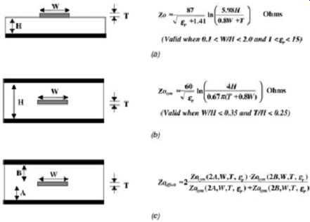
FIG. 6: Characteristic impedance approximations for typical transmission
lines: (a) microstrip line; (b) symmetrical stripline; (c) offset stripline.
3.2. Propagation Velocity, Time, and Distance
Electrical signals on a transmission line will propagate at a speed that depends on the surrounding medium. Propagation delay is usually measured in terms of seconds per meter and is the inverse of the propagation velocity. The propagation delay of a transmission line will increase in proportion to the square root of the surrounding dielectric constant. The time delay of a transmission line is simply the amount of time it takes for a signal to propagate the entire length of the line. The following equations show the relationships between the dielectric constant, the propagation velocity, the propagation delay, and the time delay:
(2)
(3)
(4)
where ...
--
v = propagation velocity, in meters/second
c = speed of light in a vacuum (3 × 10^8 m/s)
er = dielectric constant
PD = propagation delay, in seconds per meter
TD = time delay for a signal to propagate down a transmission line of length x
x = length of the transmission line, in meters
The time delay can also be determined from the equivalent circuit model of the transmission line:
(5)
…where L is the total series inductance for the length of the line and C is the total shunt capacitance for the length of the line.
It should be noted that equations (2) through (4) assume that no magnetic materials are present, such that µr = 1, and thus effects due to magnetic materials can be left out of the formulas.
The delay of a transmission line depends on the dielectric constant of the dielectric material, the line length, and the geometry of the transmission line cross section. The cross-sectional geometry determines whether the electric field will stay completely contained within the board or fringe out into the air. Since a typical PCB board is made out of FR4, which has a dielectric constant of approximately 4.2, and air has a dielectric constant of 1.0, the resulting "effective" dielectric constant will be a weighted average between the two. The amount of the electric field that is in the FR4 and the amount that is in the air determine the effective value.
When the electric field is completely contained within the board, as in the case of a stripline, the effective dielectric constant will be larger and the signals will propagate more slowly than will externally routed traces. When signals are routed on the external layers of the board as in the case of a microstrip line, the electric field fringes through the dielectric material and the air, which lowers the effective dielectric constant; thus the signals will propagate more quickly than those on an internal layer.
The effective dielectric constant for a microstrip is calculated as follows:
(6)
(7)
where er is the dielectric constant of the board material, H the height of the conductor above the ground plane, W the conductor width, and T the conductor thickness.
3.3. Equivalent Circuit Models for SPICE
Simulation In Sect. 3 we introduced the equivalent distributed circuit model of a transmission line, which consisted of an infinite number of RLCG segments cascaded together. Since it’s not practical to model a transmission line with an infinite number of elements, a sufficient number can be determined based on the minimum rise or fall time used in the simulation.
When simulating a digital system, it’s usually sufficient to choose the values so that the time delay of the shortest RLCG segment is no larger than one-tenth of the minimum system rise or fall time. The rise or fall time is defined as the amount of time it takes a signal to transition between its minimum and maximum magnitude. Rise times are typically measured between the 10 and 90% values of the maximum swing. For example, if a signal transitioned from 0 V to 1 V, its rise time would be measured between the times when the voltage reaches 0.1 and 0.9 V.
RULE OF THUMB: Choosing a Sufficient Number of RLCG Segments
When using a distributed RLCG model for modeling transmission lines, the number of RLCG segments should be determined as follows:
...where x is the length of the line, v the propagation velocity of the transmission line, and Tr the rise (or fall) time. Each parasitic in the model should be scaled by the number of segments. For example, if the parasitics are known per unit meter, the maximum values used for a single segment must be…
Example 1: Creating a Transmission Line Model.
Create an equivalent circuit model of a loss-free 50-ohm transmission line 5 in. long for the cross section shown in FIG. 7a. Assume that the driver has a minimum rise time of 2.5 ns. Assume a dielectric constant of 4.5.
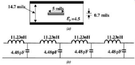
FIG. 7: Creating a transmission line model: (a) cross section; (b) equivalent
circuit. SOLUTION: Initially, the inductance and capacitance of the transmission
line must be calculated. Since no field solver is available, the equations
presented above will be used.
If the transmission line is a microstrip, the same procedure is used to calculate the velocity, but with the effective dielectric constant as calculated in equation (6). Since and , we have two equations and two unknowns. Solve for L and C.
The L and C values above are the total inductance and capacitance for the 5-in. line.
Because 3.6 is not a round number, we will use four segments in the model.
The final loss-free transmission line equivalent circuit is shown in FIG. 7b.
Double check to ensure that the rule of thumb is satisfied.
4. LAUNCHING INITIAL WAVE AND TRANSMISSION LINE REFLECTIONS
The characteristics of the driving circuitry and the transmission line greatly affect the integrity of a signal being transmitted from one device to another. Subsequently, it’s very important to understand how the signal is launched onto a transmission line and how it will look at the receiver. Although many parameters will affect the integrity of the signal at the receiver, in this section we describe the most basic behavior.
4.1. Initial Wave
When a driver launches a signal onto a transmission line, the magnitude of the signal depends on the voltage and source resistance of the buffer and the impedance of the transmission line. The initial voltage seen at the driver will be governed by the voltage divider of the source resistance and the line impedance. FIG. 8 depicts an initial wave being launched onto a long transmission line. The initial voltage Vi will propagate down the transmission line until it reaches the end. The magnitude of Vi is determined by the voltage divider between the source and the line impedance: (8)
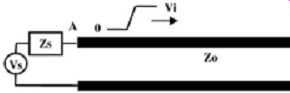
FIG. 8: Launching a wave onto a long transmission line.
If the end of the transmission line is terminated with an impedance that exactly matches the characteristic impedance of the line, the signal with amplitude Vi will be terminated to ground and the voltage Vi will remain on the line until the signal source switches again. In this case the voltage Vi is the dc steady-state value. Otherwise, if the end of the transmission line exhibits some impedance other than the characteristic impedance of the line, a portion of the signal will be terminated to ground and the remainder of the signal will be reflected back down the transmission line toward the source. The amount of signal reflected back is determined by the reflection coefficient, defined as the ratio of the reflected voltage to the incident voltage seen at a given junction. In this context, a junction is defined as an impedance discontinuity on a transmission line. The impedance discontinuity could be a section of transmission line with different characteristic impedance, a terminating resistor, or the input impedance to a buffer on a chip. The reflection coefficient is calculated as:
(9)
…impedance of the line, and Zt the impedance of the discontinuity. The equation assumes that the signal is traveling on a transmission line with characteristic impedance Zo and encounters an impedance discontinuity of Zt. Note that if Zo = Zt, the reflection coefficient is zero, meaning that there is no reflection. The case where Zo = Zt is known as matched termination.
As depicted in FIG. 9, when the incident wave hits the termination Zt, a portion of the signal, Vi?, is reflected back toward the source and is added to the incident wave to produce a total magnitude on the line of Vi? + Vi. The reflected component will then travel back to the source and possibly generate another reflection off the source. This reflection and counter-reflection continues until the line has reached a stable condition.
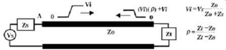
FIG. 9: Incident signal being reflected from an unmatched load. FIG. 10
depicts special cases of the reflection coefficient. When the line is terminated
in a value that is exactly equal to its characteristic impedance, there is
no discontinuity, and the signal is terminated to ground with no reflections.
With open and shorted loads, the reflection is 100%, however, the reflected
signal is positive and negative, respectively.
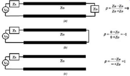
FIG. 10: Reflection coefficient for special cases: (a) terminated in Zo;
(b) short circuit; (c) open circuit.
4.2. Multiple Reflections
As described above, when a signal is reflected from an impedance discontinuity at the end of the line, a portion of the signal will be reflected back toward the source. When the reflected signal reaches the source, another reflection will be generated if the source impedance does not equal that of the transmission line. Subsequently, if an impedance discontinuity exists on both sides of the transmission line, the signal will bounce back and forth between the driver and receiver. The signal reflections will eventually reach steady state at the dc solution.
For example, consider FIG. 11, which shows one example for a time interval of a few TD (where TD is the time delay of the transmission line from source to load). When the source transitions to Vs, the initial voltage on the line, Vi, is determined by the voltage divider Vi = VsZo/(Zo + Rs). At time t = TD, the incident voltage Vi arrives at the load Rt. At this time a reflected component is generated with a magnitude of ?BVi , which is added to the incident voltage Vi, creating a total voltage at the load of Vi + ?BVi (?B is the reflection coefficient looking into the load). The reflected portion of the wave (?BVi ) then travels back to the source and at time t = 2TD generates a reflection off the source determined by ?A?BVi (?A is the reflection coefficient looking into the source). At this time the voltage seen at the source will be the previous voltage (Vi ) plus the incident transient voltage from the reflection (?BVi) plus the reflected wave (?A?BVi ). This reflecting and counter-reflecting will continue until the line voltage has approached the steady-state dc value. As the reader can see, the reflections could take a long time to settle out if the termination is not matched and can have some significant timing impacts.
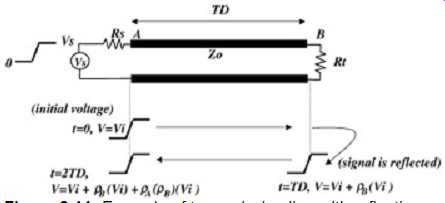
FIG. 11: Example of transmission line with reflections.
It’s apparent that hand calculation of multiple reflections can be rather tedious. An easier way to predict the effect of reflections on a signal is to use a lattice diagram.
Lattice Diagrams and Over-and Under-driven Transmission Lines.
A lattice diagram (sometimes called a bounce diagram) is a technique used to solve the multiple reflections on a transmission line with linear loads. FIG. 12 shows a sample lattice diagram. The left-and right-hand vertical lines represent the source and load ends of the transmission line. The diagonal lines contained between the vertical lines represent the signal bouncing back and forth between the source and the load. The diagram progressing from top to bottom represents increasing time. Notice that the time increment is equal to the time delay of the transmission line. Also note that the vertical bars are labeled with reflection coefficients at the top of the diagram. These reflection coefficients represent the reflection between the transmission line and the load (looking into the load from the line) and the reflection coefficient looking into the source. The lowercase letters represent the magnitude of the reflected signal traveling on the line, the uppercase letters represent the voltages seen at the source, and the primed uppercase letters represent the voltage seen at the load end of the line. For example, referring to FIG. 12, the near end of the line will be held at a voltage of A volts for a duration of 2N picoseconds, where N is the time delay (TD) of the transmission line. The voltage A is simply the initial voltage V_initial , which will remain constant until the reflection from the load reaches the source. The voltage A' is simply the voltage a plus the reflected voltage b. The voltage B is the sum of the incident voltage a, the signal reflected from the load b, the signal reflected off the source c, and so on. The reflections on the line eventually reach the steady-state voltage of the source, Vs, if the line is open.
However, if the line is terminated with a resistor, Rt, the steady-state voltage is computed as (10).
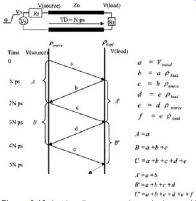
FIG. 12: Lattice diagram used to calculate multiple reflections on a transmission
line.
Example 2: Multiple Reflections for an Underdriven Transmission Line.
As described above, when the driver launches a signal onto the transmission line, the initial voltage present on the transmission line will be governed by the voltage divider between the driver impedance Zs and the line impedance Zo. As shown in FIG. 13, this value is 0.8 V. The initial signal, 0.8 V, will travel down the line until it reaches the load. In this particular case, the load is open and thus has a reflection coefficient of 1. Subsequently, the entire signal is reflected back toward the source and is added to the incident signal of 0.8 V. So at time = TD, 250 ps in this example, the signal seen at the load is 0.8 + 0.8, or 1.6 V. The 0.8 V reflected signal will then propagate down the line toward the source. When the signal reaches the source, part of the signal will be reflected back toward the load. The magnitude of the reflected signal depends on the reflection coefficient between the line impedance Zo and the source impedance Zs. In this example the value reflected toward the load is (0.8 V)(0.2), which is 0.16 V. The reflected signal will be added to the signal already present on the line, which will give a total magnitude of 1.76 V, with the reflected portion of 0.16 V traveling to the load. This process is repeated until the voltage reaches a steady-state value of 2 V.
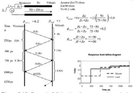
FIG. 13: Example 2: Lattice diagram used to calculate multiple reflections
for an under-driven transmission line. The response of the lattice diagram
is shown in the lower corner of FIG. 13. A computer simulation of the response
is shown in FIG. 14 for comparison. Notice how the reflections give the waveform
a "stair-step" appearance at the receiver, even though the unloaded
output of the voltage source is a square wave. This effect occurs when the
source impedance Zs is larger than the line impedance Zo and is referred
to as an underdriven transmission line.
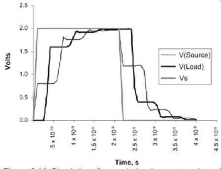
FIG. 14: Simulation of transmission line system shown in Example 2, where
the line impedance is less than the source impedance (underdriven transmission
line).
Example 3: Multiple Reflections for an Overdriven Transmission Line.
When the line impedance is greater than the source impedance, the reflection coefficient looking into the source will be negative, which will produce a "ringing" effect. This is known as an overdriven transmission line. The lattice diagram for an overdriven transmission line is shown in FIG. 15. FIG. 16 is a SPICE simulation showing the response of the system depicted in FIG. 15.
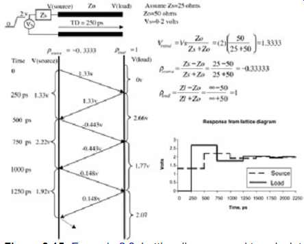
FIG. 15: Example 3: Lattice diagram used to calculate multiple reflections
for an overdriven transmission line.
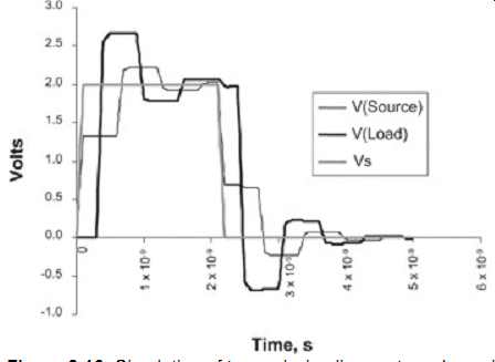
FIG. 16: Simulation of transmission line system shown in Example 3 where
the line impedance is greater than the source impedance (over-driven transmission
line).
Next, consider the transmission line structure depicted in FIG. 17. The
structure consists of two segments of transmission line cascaded in series.
The first section is of length X and has a characteristic impedance of Zo1
ohms. The second section is also of length X and has an impedance of Zo2
ohms. Finally, the structure is terminated with a value of Rt. When the signal
encounters the Zo1/Zo2 impedance junction, part of the signal will be reflected,
as governed by the reflection coefficient, and part of the signal will be
transmitted, as governed by the transmission coefficient:
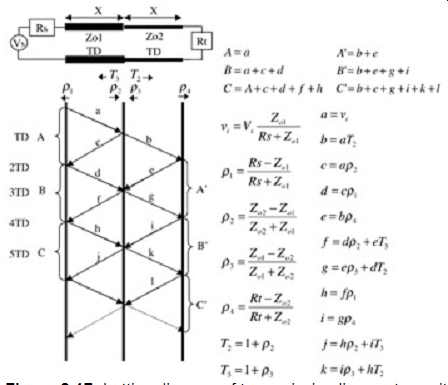
FIG. 17: Lattice diagram of transmission line system with multiple line
impedances.
FIG. 17 also depicts how a lattice diagram can be used to solve for multiple reflections on a transmission line system with more than one characteristic impedance. Note that the transmission lines in this example are of equal length, which simplifies the problem because the reflections on each section will be in phase. For example, refer to FIG. 17 and note that the reflection, e, adds directly to the reflection, f. When the two transmission lines are of different lengths, the reflections from one section won’t be in phase with the reflections from the other section, which complicates the diagram drastically. Once the system complexity progresses beyond the point depicted in FIG. 17, it’s preferable to use a simulator such as SPICE to solve the system.
Bergeron Diagrams and Reflections from Nonlinear Loads.
The Bergeron diagram. is another technique used for solving multiple reflections on a transmission line. A Bergeron diagram is used in place of a lattice diagram when nonlinear loads and sources exist in the system. A good example of when a Bergeron diagram is necessary is when a transmission line is terminated with a clamping diode to prevent excess signal overshoot or damage due to electrostatic discharge. Furthermore, output buffers rarely exhibit perfectly linear I-V characteristics; thus a Bergeron diagram will give a more accurate representation of the reflections if the I-V characteristics of the buffers are well known.
Refer to FIG. 18. To construct a Bergeron diagram, plot the I-V characteristics of the load and the source. The source I-V curve will have a negative slope of 1/Rs since current is leaving the node and the X intercept will be at Vs. Then, beginning with the transmission line's initial condition (i.e., V = 0, I = 0), construct a line with a slope of 1/Zo. The point where this line intersects the source I-V curve gives the initial voltage and current on the line at the source at time = 0. You may recognize this as a load diagram. From the intersection with the source line, construct a line with a slope of -1/Zo and extend the line to the load curve. This vector represents the signal traveling down the line toward the load. The intersection with the load line will define the voltage and current at the load at time = TD, where TD is the time delay of the line. Repeat this procedure using alternating slopes of 1/Zo and -1/Zo until the transmission line vectors reach the point where the load and source lines intersect. The intersections of the transmission line vectors and the load and source I-V curves give the voltage and current values at steady state. FIG. 19 is an example that calculates the response of a similar system where Vs = 3 V, TD = 500 ps, Zo = 50 ?, Rs = 25 ?, and the diode behaves with the equation shown.
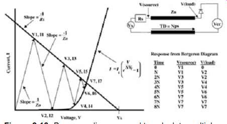
FIG. 18: Bergeron diagram used to calculate multiple reflection with a
nonlinear load.
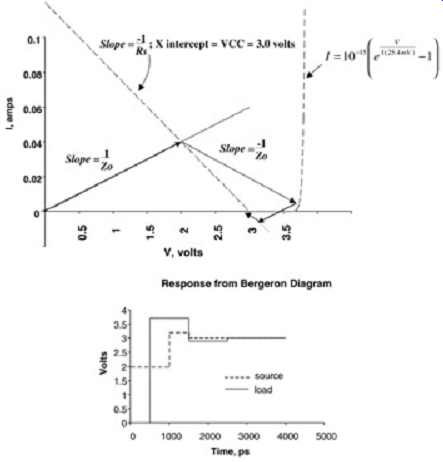
FIG. 19: Bergeron diagram used to calculate the reflection on a transmission
line with a diode termination.
POINT TO REMEMBER
Use a Bergeron diagram to calculate the reflections on a transmission line when either the source or load exhibits significant nonlinear I-V characteristics.
4.3. Effect of Rise Time on Reflections
The rise time will begin to have a significant effect on the wave shape when it becomes less than twice the delay (TD) of the transmission line. Figures 20 and 21 show the effect that edge rate has on underdriven and overdriven transmission lines. Notice how significantly the wave shape changes as the rise time exceeds twice the delay of the line. When the edge rate exceeds twice the line delay, the reflection from the source arrives before the transition from one state to another is complete (i.e., high-to-low or low-to-high transition).
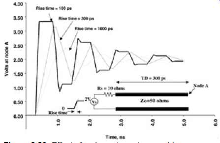
FIG. 20: Effect of a slow edge rate: overdriven case.
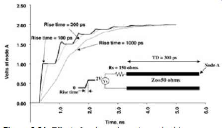
FIG. 21: Effect of a slow edge rate: underdriven case.
4.4. Reflections from Reactive Loads
In real systems there are rarely cases where the loads are purely resistive. The input to a CMOS gate, for example, tends to be capacitive. Additionally, bond wires and the lead frames of the chip packages are quite inductive. This makes it necessary to understand how these reactive elements affect the reflections in a system. In this section we introduce the effect that capacitors and inductors have on reflections. This knowledge will be used as a basis in future Sections, where capacitive and inductive parasitic effects are explored in more detail.
Reflections from a Capacitive Load.
When a transmission line is terminated in a reactive element such as a capacitor, the waveforms at the driver and load will have a shape quite different from that of the typical transmission line response. Essentially, a capacitor is a time-dependent load, which will initially look like a short circuit when the signal reaches the capacitor and will look like an open circuit after the capacitor is fully charged. Let's consider the reflection coefficient at time = TD and at time = t1. At time = TD, which is the time when the signal has propagated down the line and has reached the capacitive load, the capacitor won’t be charged and will look like a short circuit. As described earlier in the Section, a short circuit will have a reflection coefficient of -1. This means that the initial wave of magnitude V will be reflected off the load with a magnitude of -V, yielding an initial voltage of 0 V. The capacitor will then begin to charge at a rate dependent on t, which is the time constant of an RC circuit, where C is the termination capacitor and R is the characteristic impedance of the transmission line.
Once the capacitor is fully charged, the reflection coefficient will be 1 since the capacitor will resemble an open circuit. The voltage at the capacitor beginning at time t = TD is governed by...
(12)
(13)
FIG. 22 shows a simulation of the response of a line terminated with a capacitive load.
The load capacitance is 10 pF, the line length is 3.5 in. (TD = 500 ps), and the driver and transmission line impedance are both 50 ?. Notice the shape of the waveform at the source (node A). It dips toward 0 at 1 ns, which is 2TD, the time that the reflection from the load arrives at the source. It dips toward zero because the initial reflection coefficient off the capacitor is -1, so the voltage reflected back toward the source is initially Vi + (-Vi ), where Vi is the initial voltage launched onto the transmission line. The capacitor then charges to a steady-state value of 2 V.
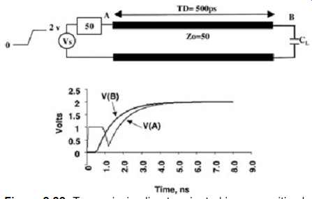
FIG. 22: Transmission line terminated in a capacitive load.
If the line is terminated with a parallel resistor and capacitor, as depicted in FIG. 23, the voltage at the capacitor will depend on and the time constant will depend on the CL and the parallel combination of RL and Zo:
(15)
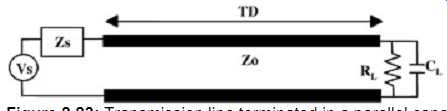
FIG. 23: Transmission line terminated in a parallel capacitive and resistive
load.
Reflection from an Inductive Load.
When a series inductor appears in the electrical pathway on a transmission line, as depicted in FIG. 24, it will also act as a time-dependent load. Initially, at time = 0, the inductor will resemble on open circuit. When a voltage step is applied initially, almost no current flows across the inductor. This produces a reflection coefficient of 1. The value of the inductor will determine how long the reflection coefficient will remain 1. If the inductor is large enough, the signal will double in magnitude. Eventually, the inductor will discharge its energy at a rate that depends on the time constant t of an LR circuit, which will have a value of L/Zo. FIG. 25 shows the reflections from four different values of the series inductor depicted in FIG. 24. Notice that the magnitude of the reflection and the decay time increased with increasing inductor value.
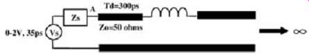
FIG. 24: Series inductor.
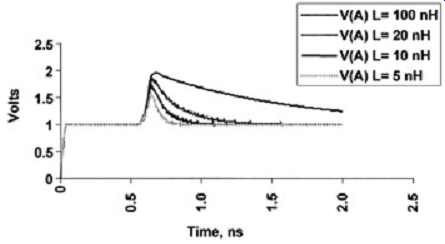
FIG. 25: Reflection as seen at node A of FIG. 24 for different inductor
values.
4.5. Termination Schemes to Eliminate Reflections
As explained in later Sections, reflections on a transmission line can have a significant negative impact on the performance of a digital system. To minimize the negative impact of the reflections, methods must be developed to control them. Essentially, there are three ways to mitigate the negative impact of these reflections. The first method is to decrease the frequency of the system so that the reflections on the transmission line reach steady state before another signal is driven onto the line. This is usually impossible, however, for high speed systems since it requires decreasing the operating frequency, producing a low-speed system. The second method is to shorten the PCB traces so that the reflections will reach steady state in a shorter time. This is usually not practical since doing so generally involves using a PCB board with a greater number of layers, which increases cost significantly.
Additionally, shortening the traces may be physically impossible in some cases. These first two methods always have a limit at which the bus frequency increases to a point where the reflections won't reach steady state in one period. The third method is to terminate the transmission line with an impedance equal to the characteristic impedance of the line at either end of the transmission line and eliminate the reflections.
When the source end of the transmission line is designed to match the characteristic impedance of the transmission line, the bus is said to be source terminated. When a bus is source terminated, any reflections produced by a large impedance discontinuity at the far end of the line (such as an open circuit) are eliminated when they reach the source because the reflection coefficient will be zero. When a terminating resistor is placed at the far end of the line, the bus is said to be parallel, or load terminated. Multiple reflections will be eliminated at the load because the reflection coefficient at the load is zero. There are several different ways to implement these termination methodologies. There are advantages and disadvantages to each technique. Several techniques are summarized in the following sections.
On-Die Source Termination
On-die source termination requires that the I-V curve of the output buffer be very linear over the operating range and yield an I-V curve with an impedance very close to the transmission line impedance. Ideally, this is an optimum solution because it does not require any additional components that increase cost and consume area on the board. However, since there are numerous variables that drastically affect the output impedance of a buffer, it’s difficult to achieve a good match between the buffer impedance and the line impedance.
Some of the variables that affect the buffer impedance are silicon fabrication process variations, voltage, temperature, power delivery factors, and simultaneous switching noise.
These variations will make it difficult to guarantee that the buffer impedance will match the line impedance. FIG. 26 depicts this termination method.
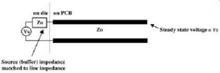
FIG. 26: On-die source termination.
Series Source Termination.
Series source termination requires that a resistor be added in series with the output buffer.
FIG. 27 depicts the implementation of a series source termination. This type of termination requires that the sum of the buffer impedance and the value of the resistor be equal to the characteristic impedance of the line. This is usually best achieved by designing the I-V curve of the output buffer to yield a very low impedance such that the bulk of the impedance looking into the source will be contained in the resistor. Since precision resistors can be chosen, the effect of the on-die impedance variation due to process and environmental variations on the silicon that make on-die source termination difficult can be minimized. The total variation in impedance will be small because the resistor, rather than the output buffer itself, will comprise the bulk of the impedance. The disadvantages of this technique are that the resistors add cost to the board, and it consumes significant board area.
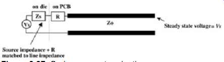
FIG. 27: Series source termination.
Load Termination with a Resistive Load.
Load or parallel termination with a resistive load eliminates the unknown variables associated with the buffer impedance because a precision resistor can be used. The reflections are eliminated at the load and low-impedance output buffers may be used. The disadvantage is that a large portion of the dc current will be shunted to ground, which exacerbates power delivery and thermal problems. The steady-state voltage will also be determined from the voltage divider between the source resistance and the load resistance, which creates the need for stronger buffers. Power delivery is a difficult problem to solve in modern computers. Laptops, for example, need very efficient power delivery systems since they require the use of batteries over prolonged periods of time. As power consumption increases, cost also increases, because more elaborate cooling mechanisms must be introduced to dissipate the excess heat. FIG. 28 depicts this termination scheme.
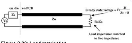
FIG. 28: Load termination.
AC Load Termination
Ac load termination uses a series capacitor and resistor at the load end of a transmission line to eliminate the reflections. The resistor R should be equal to the characteristic impedance of the transmission line, and the capacitor CL should be chosen such that the RC time constant at the load is approximately equal to one or two rise times. It’s advised that simulations be performed to choose the optimum capacitor value for the specific design. The premise behind this termination scheme is that the capacitor will initially act like a short circuit and the line will be terminated in its characteristic impedance by the resistor R for the duration of the rising or falling edge. The capacitor will then charge up and the steady-state voltage of the source, Vs, will be reached. The advantage of this technique is that the reflections are eliminated at the load with no dc power dissipation. The disadvantages are that the capacitive loading will increase the signal delay by slowing down the rising or falling times at the load. Furthermore, the additional resistors and capacitors consume board area and increase cost. FIG. 29 depicts this termination scheme.
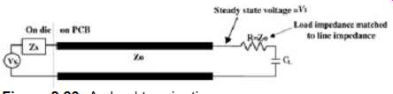
FIG. 29: AC load termination.
Common Termination Problems
One of the common obstacles encountered during bus design is that the characteristic impedance of the trace tends to vary significantly, due to PCB production variations. The PCB variation affects all the termination methods; however, it tends to have a bigger impact on source termination. Typical, low-cost PCB boards, for example, usually vary as much as ±15% from the target impedance over process. This means that if an engineer specifies a 65-? impedance for the lines on a PCB board, the vendor will guarantee that the impedance will be within 55.25 ? (65 ? - 15%) and 74.75 ?(65 ? + 15%). Finally, crosstalk will introduce additional variations in the impedance. The impact of the crosstalk-induced variations will depend on trace-to-trace spacing, the dielectric constant, and the cross-sectional geometry.
Crosstalk is discussed thoroughly in Section 3.
For short lines, when the minimum digital pulse width is long compared to the time delay (TD) of the transmission line, source termination is desirable since it eliminates the need to shunt a portion of the driver current to ground. For long lines, where the width of the digital pulse is smaller than the time delay (TD) of the line, load termination is preferable. In the latter case, there will be multiple signals traveling down the transmission line at any given time (this is known as pipeline mode). Since reflections off the load will reflect back toward the source and interfere with the signals propagating down the line, the reflections must be eliminated at the load.
5. ADDITIONAL EXAMPLES
5.1. Problem
Assume that two components, U1 and U2, need to communicate with each other via a high speed digital bus. The components are mounted on a standard four-layer motherboard with the stackup shown in FIG. 30. The driving buffers on component U1 have an impedance of 30 ?, an edge rate of 100 ps, and a swing of 0 to 2 V. The traces on the PCB are required to be 50 ? and 5 in. long. The relative dielectric constant of the board (er) is 4.0, the transmission line is assumed to be a perfect conductor, and the receiver capacitance is small enough to be ignored. FIG. 31 depicts the circuit topology.
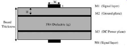
FIG. 30: Standard four layer motherboard stackup.
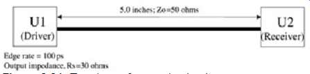
FIG. 31: Topology of example circuits.
5.2. Goals
Determine the correct cross-sectional geometry of the PCB shown in FIG. 30 that will yield an impedance of 50 ohm.
Calculate the time it takes for the signal to travel from the driver, U1, to the receiver, U2.
Determine the wave shape seen at U2 when the system is driven by U1.
Create an equivalent circuit of the system.
5.3. Calculating the Cross-Sectional Geometry of the PCB
Since the signal lines on the stackup depicted in FIG. 30 are microstrips, the cross sectional geometry can be determined from the equations in FIG. 6. The fact that some of the microstrip lines are referencing a power plane instead of a ground plane should not cause confusion. For the purpose of transmission line design, a dc power plane will act like an ac ground and is treated as a ground plane in transmission line design. The consequences of this approximation are examined in subsequent Sections. FIG. 6 shows that the trace impedance is a function of H, W, t, and er (see FIG. 30):
++++++++++++++++++++
The standard metal thickness of microstrip layers on a PCB board is usually on the order of 1.0 mil. Since the desired impedance, dielectric constant er, and the thickness are known, this leaves one equation and two unknowns. Subsequently, one value of either H or W needs to be chosen. Typical PCB manufacturers will usually deliver a minimum trace width of 5 mils. Since small trace widths use up less board real estate, which allows the PCB to be physically smaller and less expensive, the minimum trace width of 5.0 mils is chosen.
Plugging the known values of er, W, t, and Zo into the equation above and solving for H yields.
FIG. 32 depicts the resulting stackup of the PCB.
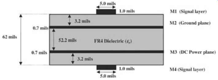
FIG. 32: Resulting PCB stackup resulting in 50-ohm transmission lines.
Note the thickness of the inner metal and dielectric layers. The internal metal layers are only 0.7 mil thick instead of 1.0 mil thick. This is because the outer layers are usually tinplated to stop the outer copper traces, which are exposed to the environment, from oxidizing. The inner traces are not plated. Since a typical PCB board thickness requested by industry is 62 mils thick, the thickness of the dielectric layers between the power and ground plane is increased to achieve the desired board thickness.
5.4. Calculating the Propagation Delay
To calculate the time it takes for the signal to travel from U1 to U2, it’s necessary to determine the propagation velocity for a signal traveling on the transmission line that was just designed. Since the transmission line is a microstrip, the effective dielectric constant must be used to calculate the propagation velocity. The effective dielectric constant is calculated using equations (6) and (7).
Since W/H = 5/3.2 > 1.0, then F = 0. Therefore, ...
The propagation velocity is determined using equation (2).
The time delay for the signal to propagate down the 5-in. line connecting U1 and U2 is then calculated using equation (4).
5.5. Determining the Wave Shape Seen at the Receiver
The easiest way to calculate the wave shape seen at the receiver is to use a lattice (or bounce) diagram ( FIG. 33). It should be noted that a Bergeron diagram could also be used; however, since there is no nonlinear device at the receiver such as a diode, the lattice diagram is the preferred method of analysis. Refer to Sect. 4.
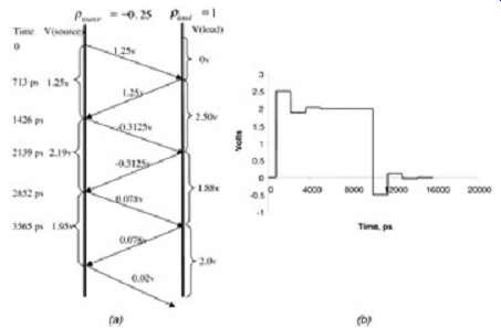
FIG. 33: Determining the wave shape at the receiver: (a) lattice diagram;
(b) wave form at U2 when U1 is driving. ... where Rs is the buffer impedance
of U1 and Rload is the open circuit seen at U2 (this assumes that the input
capacitance to the buffer is very small, i.e., 2 to 3 pF).
5.6. Creating an Equivalent Circuit
To create the equivalent circuit model for this example, it’s first necessary to determine the number of LC segments required. This is done using the rule of thumb presented in Sect. 3. To do so, it’s convenient to convert the velocity calculated earlier to the units of inches/picosecond:
Therefore, the minimum of 72 segments is required to create an accurate transmission line model.
Now the equivalent inductance and capacitance per unit inch is calculated using equations (1) and (5). Since this particular example is loss-free (i.e., a perfect conductor is assumed), equation (1) is reduced to . The delay per unit inch is TD = 713 ps/5.0 in. = 142.6 ps/in. = , where L and C are per unit inch.
The equivalent L and C per unit inch are calculated by solving TD and Zo for L and C.
Now, referring back to the rule of thumb presented in Sect. 3, the L and C per segment are calculated.
To double check the calculations, the impedance and delay per segment can be calculated:
The equivalent circuit of the transmission line is then constructed of 72 LC segments. The driving buffer at U1 is depicted as a simple voltage source and a series resistor. The open circuit at the end of the line is approximated with a very large resistor ( FIG. 34).
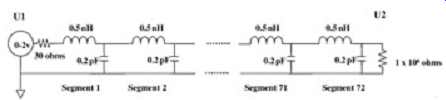
FIG. 34: Final equivalent circuit.