AMAZON multi-meters discounts AMAZON oscilloscope discounts
5. ODD- AND EVEN-MODE IMPEDANCE
Differential impedance measurements are required to extract the odd-mode impedance between two signal lines that are coupled. To complete differential measurements, two TDR sources need to be injected across a pair of coupled signal lines simultaneously. The TDR output edges must be phase aligned so that the output edges have zero time delay (skew) between them. After aligning the edges, reverse the polarity on one source to measure the odd-mode impedance or leave the polarity the same to extract the even-mode impedance.
An example of this is shown in FIG. 21.
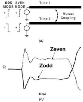
FIG. 21: Example of a TDR response for a differential impedance measurement
of two traces left open. (a) differential measurement setup (requires
two simultaneous sources that are phase aligned in time); (b) differential
TDR response.
6. CROSSTALK NOISE
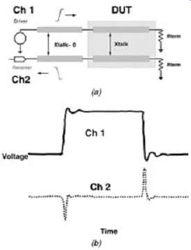
FIG. 22: Example of (a) a basic crosstalk measurement setup along with
(b) the response.
Another important parameter that must be characterized in high-speed design is the voltage induced on adjacent lines due to crosstalk. Similar to differential impedance measurements, crosstalk is measured utilizing two or more channels. A common method used to evaluate crosstalk is to measure the noise induced on a passive line due to the neighbor or neighbors.
For this case, two coupled lines will be examined.
Crosstalk can be measured as illustrated in FIG. 22 by injecting the TDR pulse into a line and measuring the noise induced on the victim line. The chart shown in here will relate the magnitude and shape of the crosstalk pulses for a two-line system to the mutual parasitics, input step voltage, edge rate, and victim termination.
Completing simulations of the same net can be done to compare modeling accuracy against lab data. Filtering functions can be implemented to examine noise for slower rise times to emulate system bus speeds. Filtering functions are predominantly digital filters that postprocess the data received within the TDR instrument. The use of passive filters inserted inline are not recommended.
7. PROPAGATION VELOCITY
Measurement of propagation delay and velocity is more difficult than measuring impedance.
For velocity, the structure delay is determined by measuring the difference in time that it takes the pulse to propagate through the structure. Measurement points for propagation delays are difficult to choose and accuracy is extremely dependent on the probing technique.
The most accurate delay measurements require advanced probing techniques that utilize controlled-impedance microprobes with the TDR in time-domain transmission (TDT) mode.
This improved accuracy comes at a cost of equipment and time. Selecting the method for measuring the velocity depends on the accuracy desired and the amount of time allotted for measurement. It should be noted that velocity measurements are to be used to extract the effective dielectric constant as shown with equations (2.3) and (2.4). 11.7.1. Length Difference Method
The simplest method for measuring propagation delay is using TDR mode to measure delay between two identical test structures of different length (TDR mode assumes that the user is looking only into the near end of the DUT). Velocity is determined by subtracting the reflected delay differences between the two structures. As shown in FIG. 23, the delta T value will be twice the actual delay difference due to reflection delay down and back. The velocity per unit length is calculated as (8)
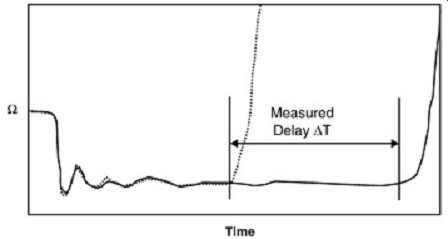
FIG. 23: Example of a TDR propagation delay measurement for two identical
impedance coupons that differ only in length. The purpose of using two
test structures is to cancel out errors in the determination of the point
where the waveform begins to rise due to the open circuit at the far end
of the DUT. Accuracy will depend on probes and structure. To make this
measurement, maximize the TDR time base and position the cursors at the
point where the reflected pulse begins to rise, as illustrated in FIG.
23.
7.2. Y-Intercept Method
If space permits, the approach described above can be improved by using three test structures of different length. To calculate the velocity, plot length versus delay (length on the x-axis). Draw a line that that best fits the data (if the measurements are taken consistently, the three points should lie on a straight line). The inverse of the slope will be the propagation velocity. If the measurement is perfect, the line will intercept the y-axis at zero. Otherwise, the actual y-axis intercept gives the measurement error.
7.3. TDT Method
Improved accuracy of propagation delay measurements can be completed with the TDR used in TDT mode (TDT means that the signal is also observed at the far end of the line). In this method, probes are placed at each end of the test structure. A pulse is injected into one end and captured at the other end. This approach has less edge-rate degradation than the simpler methods already mentioned, which results in improved accuracy. The measurement is completed by injecting the pulse on one end of the test coupon with a 50 ohm probe and capturing the signal at both the launch point and the open end with a low-capacitance high bandwidth high-impedance probe (10× or 20×), as illustrated in FIG. 24. The advantage of this technique over the TDR is that the captured signal has propagated only once down the coupon when it is captured, which will allow less time for the edge rate to be degraded by losses or reflections.
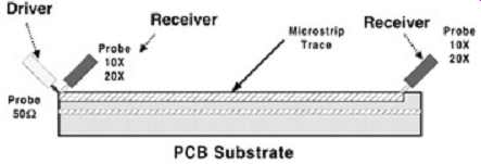
FIG. 24: Example of a basic TDT measurement setup for evaluating propagation
velocity of a microstrip trace.
The measurements are completed by connecting the 50 ohm probe to a sampling head with the TDR/TDT mode "ON." The high-impedance probes should be connected to separate channels and with the head function's TDR/TDT setting mode to "OFF." Measure the delay between the transmitted and received signals (using the high-impedance probes at the driver and receiver). This is the propagation delay of the trace. All methods of measuring propagation velocity are highly subjective, due to where the measurement point along the response is taken. The ideal measurement point is that at which the response just begins to rise. This would eliminate the error due to different edge rate degradation if measurement were taken at, for example, the 50% point. However, in most circumstances the incident preshoot and foot characteristics can make it quite difficult to determine exactly when the response is rising [McCall, 1999].
8. VECTOR NETWORK ANALYZER
One of the prominent laboratory instruments used for radio-frequency and microwave design purposes is the vector network analyzer (VNA). A VNA is ideally suited for measuring the response of a DUT (device under test) as a function of frequency. The primary output of a VNA is reflected and transmitted power ratios or the square roots thereof. Through mathematical manipulation of the power ratios, a large amount of valuable data can be extracted. A few examples that can be measured with a VNA are skin effect losses, dielectric constant variations, characteristic impedance, capacitive and inductive variations, and coupling coefficients. Furthermore, since VNAs are typically designed with the microwave engineer in mind, they can make reliable measurements to extremely high frequencies. The primary disadvantage is that they provide data in the frequency domain. Subsequently, it is necessary to translate the extracted data into a useful format that can be used in the time domain.
In the past, most digital designs had no need for extracted electrical characteristics in the hundreds of megahertz range, simply because their operating frequencies were low compared to today's systems. Modern bus designs, however, are becoming so fast that such measurements are a necessity. As bus speeds pass the 500-MHz region, rise and fall times are required to be as fast as 100 ps. Subsequently, the frequency content of the digital waveforms can easily exceed 3 GHz. As bus frequencies increase, the resolution required for measuring capacitance, inductance, and resistance increases. To the design engineer, proper characterization to a fraction of a picofarad, for example, might be necessary to characterize the timings on a bus accurately. If used properly, the VNA is the most accurate tool available to extract the electrical parameters necessary to simulate high-speed designs.
The primary focus of this discussion is on VNA operation to extract relevant electrical parameters prominent in digital high-speed bus designs. This includes propagation delay, crosstalk, frequency-dependent resistance, capacitance, and inductance parameters. Basic procedures used to measure items such as connectors, sockets, vias, and PCB traces are covered. It should be noted that these techniques may or may not apply to the reader.
However, for the novice VNA user, these procedures should help provide some helpful concepts for utilizing the VNA to yield accurate results.
Because the focus of this Section is on validating and developing models for high-speed digital design, the measurement techniques discussed are limited to the common methods most useful for the characterization and development of models. The discussion includes measurement techniques, sources of error, and instrument calibration.
8.1. Introduction to S Parameters
The primary output of the VNA is the scattering matrix, also know as S parameters. The scattering matrix provides a means of describing a network of N ports in terms of the incident and reflected signals seen at each port. As frequencies approach the microwave range, the ability to extract voltage and currents in a direct manner becomes very difficult. Under these circumstances, the only directly measurable quantities are the voltages (or power) in terms of incident, reflected, and transmitted waves, which are directly related to the reflection and transmission coefficients at the measurement ports. Therefore, the scattering matrix is defined in terms of the reflected signals from each port of a device and the transmitted signals from one port to another, as shown in FIG. 25.
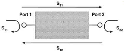
FIG. 25: Two-port junction.
The general nomenclature is this. Sij means that the power is measured at port i and injected at port j. For example, S11 is defined as the square root of the ratio between the power reflected at port 1 over the power injected into port 1. This can usually be simplified by using the voltage ratios, as shown in FIG. 26. Subsequently, S11 is defined as the reflection coefficient of the ith port if i = j and all other ports are impedance matched. Equation (9) is a simplified definition of S11 when the conditions stated above are met.
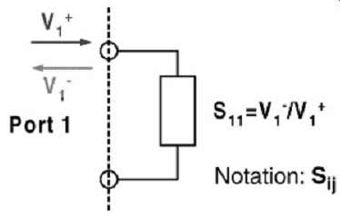
FIG. 26: S-parameter one-port definition and general notation.
The transmission coefficients, such as S21, are defined as the output voltage at port 2 over the input voltage at port 1 and can be used to measure items such as propagation delay and attenuation:
For symmetrical systems, such as a PCB trace, S22 = S11 and S12 = S21.
If the network is lossless, the S-parameters must satisfy the equation (11).
This is a useful relationship for low-loss systems and at frequencies when skin effect resistance is small. If these characteristics hold true for the DUT, the networks can be simplified greatly to reduce the calculations needed to extract the parameters.
8.2. Equipment
The VNA measurement setup needed to achieve high accuracy will require the use of controlled impedance microprobes along with their respective calibration substrate. This will therefore require a stable probe station along with optics (a microscope) to achieve good repeatable measurements that will minimize the possibility of expensive equipment damage.
8.3. One-Port Measurements (Zo, L, C)
One-port VNA measurements are useful for extracting inductance, capacitance, and impedance as a function of frequency. This is especially useful for the characterization of connectors, vias, and transmission lines. The S-parameter one-port measurement is a measure of S11 or S22.
To understand how inductance and capacitance are measured at low frequencies, consider a short section of a transmission line. A low frequency, for these applications, is when the wavelength is much larger than the length of the structure. The relationship between wavelength and frequency is _ = c/(F ), where F is the frequency, c the speed of light in free space, and er the effective dielectric constant. By solving the circuit equations we can derive the voltage and currents for a short length of open and shorted transmission line:
(12)
(13)
If we consider only the first-order effects by neglecting R and G, the two equations simplify so that a current flowing through the line will produce a voltage that is proportional to the inductance if the line is shorted to ground. Furthermore, the voltage induced between the line and ground will produce a current that is proportional to the capacitance if the line is left open ended. To understand when these approximations apply, let us first consider the case when the structure is shorted to ground. As long as the impedance of the structure capacitance is large compared to the impedance of the structure inductance at the measurement frequency, there will be minimal current flowing through the capacitor.
Subsequently, the voltage drop across the structure will be primarily a function of the inductance when the structure is shorted to ground. Now, let us consider the case when the structure is left open ended. As long as the structure is small compared to the wavelength at the measurement frequency, it will look like a lumped element capacitor. Subsequently, the structure will charge up and the current will flow to ground through the structure capacitance.
The structure inductance can be ignored as long as the wavelength is sufficiently long so that no significant transient voltage differentials can exist across the structure. As a result, under the conditions stated above, the current will depend primarily on the structure capacitance.
By opening and shorting the far end of a DUT, one-port VNA measurements (i.e., S11 or S22) are made to extract the inductance and capacitance of a short structure, such as a connector pin. If the VNA is set to display a Smith chart, as shown in FIG. 27, the inductance and capacitance values can be determined most easily. To determine the capacitance, the DUT should be open ended. To determine the inductance, the far end of the DUT should be shorted to ground.
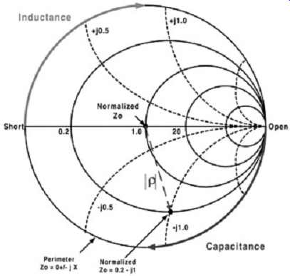
FIG. 27: Representative Smith chart highlighting the basic parameters.
A Smith chart is a graphical aid that is very useful for visualizing frequency-domain problems.
This display format is used to visualize normalized impedance (both real and imaginary parts) in terms of the reflection coefficient as a function of frequency. The normalized impedance is equivalent to the impedance of the DUT divided by the VNA system impedance, which is set during calibration. The VNA system impedance is normally 50 ohm ; however, it can be set to alternative values when necessary to provide more accurate results when the target DUT impedance is significantly different. The center point (1), shown in FIG. 27, corresponds to the VNA output impedance (1 + j0)ZVNA. The horizontal line through the center for the Smith chart corresponds to the real impedance axis, which goes from zero ohms (short) on the left-hand side through to infinite impedance (open) on the right-hand side. Furthermore, the outside perimeter equates to purely reactive impedance values such as purely capacitive or inductive loads. Several references exist explaining the Smith chart in greater detail. The reader is encouraged to learn more about the chart since it is a very useful tool. For the purposes here, only points on the perimeter of the chart will be considered.
Measuring Self-Inductance and Capacitance of a Short Structure.
To show briefly how the reactive components are extracted, let's consider a small trace or stub terminated with a short to ground (assume that the losses are negligible). Since the termination is a short, the reflection coefficient is -1 and the impedance seen will be reactive (because it will lie on the outer perimeter of the Smith chart). For low frequencies, this structure will look inductive as long as the trace is electrically shorter than _/4 of the frequency of interest. When the frequency is very low, the DUT will look almost like a pure short to ground. As the frequency increases, the impedance will increase (jwL), and the value on the Smith chart will move clockwise toward the open point, as depicted in FIG. 27.
The inductance can be calculated by observing the imaginary portion of the impedance on the Smith chart (the real part should be very small) and solving equation (14) for the inductance, where w is the angular frequency (2pF). The reader should pay close attention to whether or not the value read off the Smith chart is normalized. The VNA output may or may not be set to display normalized data. The equation (14) assumes that the VNA reading is not normalized to the VNA system impedance. If the same measurement is taken with the DUT open ended, the reflection coefficient will be 1 and the trace will look capacitive. At low frequencies, the Smith chart cursor will be very close to the open point in FIG. 27 and will move clockwise toward the short as frequency increases.
The capacitance can be calculated by observing the imaginary portion of the impedance on the Smith chart (the real part should be very small) and solving the equation (15)
for the capacitance. Again, pay attention to whether or not the data is normalized. Equation (15) assumes nonnormalized data. If the DUT exhibits significant losses, or the frequency gets high enough so that the assumptions above are violated, the trace on the Smith chart will begin to spiral inward because the impedance is no longer purely imaginary.
For more accurate results, some measurements may require two identical structures that vary only in length. For example, if there are vias on a test board that are required to interface the probe to the DUT, they may interfere with the measurement. If the parasitics of the vias, or probe pads, are significant compared to the DUT, this will cause a measurement error. If two short structures of different lengths are measured, the difference in the measured parasitics can be divided by the difference in the length to yield the inductance or capacitance per length. This will produce more accurate results because the parasitics of the probe pads and vias will be subtracted out.
Although these measurement techniques are valid only for low frequencies, the results can generally be applied to much higher frequency simulations because the capacitive and inductive characteristics of a structure (such as a socket or connector) will typically not exhibit significant variations with frequency.
Socket and Connector Characterization.
The primary metric used for characterizing a connector or a socket is the effective inductance and capacitance. As described in Section 5, the equivalent parasitics depend on the physical characteristics of the pin, but also on the pin assignment. This is illustrated in Figures 5.5 and 5.6. Subsequently, when measuring the inductance and capacitance of a connector or socket, it is imperative that the measurements be performed in such a manner so that the results reflect, or can be manipulated, so that the effective parasitics seen in the system can be obtained. To illustrate this, refer to FIG. 6a and d. Significantly more coupling to the adjacent data pins will be experienced in FIG. 6a than in FIG. 6d, whose pinout isolates the signals from each other. Although the self-inductance of the pins in this example may be identical, the effective inductance as seen in the system will be quite different.
To measure or validate the DUT, specific test boards are usually required that have open and short structures so that the capacitance and inductance can be measured. In instances when electrical values of the test structure used to interface the probe to the DUT are significant (e.g., a trace on the test board leading from the probe to the socket/connector), two different measurements are required. First, the equivalent parasitics of the trace and probe pad leading to the DUT must be determined. Next, the total structure, including the interface traces and the DUT, must be measured. By subtracting the trace parasitics from the total parasitics, the DUT self-electrical values can be determined.
An example of a connector test board is illustrated in FIG. 28. In this instance there are structures that are used to interface the microprobe to the connector. Since the goal is to extract the electrical parameters of the connector, not the interface structures on the test board, open and short measurements will need to be completed first to extract the L and C values of the test board without the connector. Next, the measurements are taken to obtain the total L and C values of the connector plus the test board. The two results are subtracted, resulting in the L and C values of the connector. This typically requires two separate test structures, one to extract the board parasitics and one to extract the total board and DUT parasitics. These structures should be placed in close proximity to each other to minimize differences across the board due to manufacturing variations.
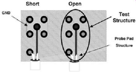
FIG. 28: Simple example of a socket test board used to measure the parasitics.
One-Port Impedance Measurement.
Impedance measurements can be calculated based on inductance and capacitance data obtained per unit length using the self-value procedures described. An alternative method is to use the VNA in TDR mode. Most VNAs have time-domain capability using the inverse FFT (fast Fourier transform) to translate the frequency-domain data to a time-domain response. When this is done, the time-domain response will be as discussed earlier in the Section for TDR. Therefore, measurements should be extracted in a similar manner. To achieve the highest accuracy, the VNA output impedance should be calibrated to the nominal design impedance. Another nice feature of using the VNA in the time domain is the ability to set the system bandwidth and thereby tune the edge rate to match the design.
Transmission Line (R, L, G, C).
Transmission line parameters can be derived from both open and short S11 measurements.
General common method for model derivation or validation is to utilize modeling software to extract the parasitics from the measured data. The measured data, in terms of magnitude and phase versus frequency, can be input into the modeling software to curve fit the frequency-domain response and thereby yield the RLCG values used to accurately model lossy, frequency-dependent models.
8.4. Two-Port Measurements (Td, Attenuation, Crosstalk)
Two-port measurements such as S21 and S12 are used to measure the forward and reverse insertion loss. This is used to measure mutual terms, attenuation, and propagation delay.
Mutual Capacitance and Inductance of an Electrically Short Structure.
The techniques presented here are very useful for measuring the mutual capacitance and inductance between two electrically short structures, such as connector or socket pins.
Again, the structure is considered short if the electrical length (delay) is much smaller than _/4.
The measurements of the mutual terms require two test structures that neighbor each other.
Care should be taken when designing the test board so that the interface traces (the traces that connect the probe to the connector) are not coupled. One common method is to angle the traces into the structure and minimize parallelism. The mutual terms are extracted in a manner similar as to that for the self-values by using open and shorted structures. Opening and shorting the far end of the two structures together will produce the simplified equivalent circuits shown in FIG. 29.
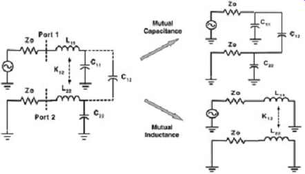
FIG. 29: Basic simplification for measuring mutual inductance and capacitance.
The two ports of the VNA are shown in FIG. 29. For the case when the circuit
is open ended, the current through the inductance will be negligible,
therefore ignored. Subsequently, the main source of coupling between ports
1 and 2 is the mutual capacitance. The mutual capacitance is extracted
with one of the following two equations:
(16)
(17)
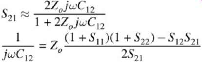
...which are derived in section D. Note that the value of S21 taken from the VNA may be in decibels and thus must be converted to linear units prior to insertion into the equations.
Equation (16) is valid when the impedance of the shunt (self) capacitors (1/jwC11) is much larger than Zo (the VNA system impedance). This usually occurs for conductors that are perpendicular to the system reference plane. If the impedance of the shunt (self) capacitance of the structure is not high compared to Zo, equation (17) may be used.
Equation (17) is derived directly from the ABCD parameters discussed in Appendix D. If each leg of the circuit is shorted to ground, the value of S21 will depend primarily on the mutual inductance. By shorting the two ends of the DUT to ground and simplifying the circuit as shown in FIG. 29, S21 can be related to the mutual inductance as (18) assuming L11 = L22 = L. Again, the derivation is shown in Appendix D. In equations (16) through (18), Zo is assumed to be the system impedance of the VNA and w = 2pF.
Propagation Velocity and Dielectric Constant.
Propagation velocity is becoming an increasingly important specification in high-speed digital designs. Modern designs require that the flight times and interconnect skews be controlled to 5 ps per inch of trace or less. Calibrated correctly, the VNA can provide a significantly more accurate characterization of the propagation delay than can be achieved with the TDR. The VNA can measure propagation delay in two different ways. The first and less accurate method is to put the VNA in time-domain mode and perform a normal TDR/TDT measurement as described earlier in the Section. For TDT measurements the data are taken by using a two-port measurement that compares the open S11 response to the S21 response.
The more accurate method is to measure the phase of the signal using a two-port measurement. This technique simply looks at the phase difference between ports 1 and 2.
The phase difference is proportional to the electrical delay of the structure. The measurement is most easily taken by displaying the data in a polar format, as shown in FIG. 30. With the VNA in polar format, the phase delay between ports 1 and 2 can be measured, which can be used to calculate the propagation delay as a function of frequency.
This is typically much more accurate than the TDR method because the VNA will output a sine wave. Losses in a system can significantly degrade the edge rate in a TDR measurement, which leads to
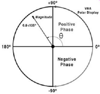
FIG. 30: Example of a polar display format (magnitude and phase) versus
frequency. Delay will be a function of phase and loss a function of magnitude.
incorrect delay measurements. As losses will degrade primarily the amplitude
of a sinusoidal signal, they will have a minimal effect on the accuracy
of the measurement.
Polar measurements are completed measuring forward S21 or reverse S12 with the VNA display in polar format. With the unit in polar format, the phase angle as a function of frequency is displayed. Adjust the marker for the frequency at which the propagation delay is desired. Delay can then be calculated using the equation (19) where F is the frequency and F is the measured phase angle. The propagation velocity is calculated with the equation (20) where x is the length of the transmission line being measured. As shown in equation (2.4), the time delay depends on both the length and the effective dielectric constant. Therefore, if the length and propagation velocity are known, the effective dielectric constant can be extracted: (21) where x is the line length and c is the speed of light in a vacuum.
Attenuation (Rac).
Attenuation measurements on a transmission line can be difficult to extract when the line impedance is different from the VNA system impedance, because reflections on the DUT will interfere with the measurement. When the system impedance is matched to the line under test, there are no reflections at the input and output port. Therefore, the value of attenuation is related simply to the magnitude of S21 or S12. When the reflections are large, mathematical manipulation of the two-port S parameters may be required. For cases when the VNA system Zo is close, or perfectly matched to the transmission line, the measurement becomes fairly simple. As a general rule of thumb, fairly accurate attenuation measurements can be extracted when the reflection coefficient is less than -20 or -25 dB: (22)
This is based on the typical noise floor of -60 dB set during calibration. This may or may not provide acceptable results, due to the varying degree of accuracy required by the user. For transmission line values that are significantly different from the standard VNA impedance of 50 ohm , it may be necessary to purchase a calibration substrate with an impedance equal to the nominal impedance of the DUT. In fact, it is advisable to purchase several calibration substrates that are compatible with the specific probe types used that are in 5-? increments.
This will allow the user to calibrate the VNA to whatever impedance is required. When the calibration substrates are not available, it is possible to make the measurements with the VNA calibrated to its nominal impedance of 50 ohm and mathematically normalize the data to the characteristic impedance of the transmission line under test. This technique is generally less accurate because small imperfections in the calibration tend to be amplified in the calculation. However, if a calibration substrate of the proper impedance is not available, it may be necessary. This technique is outlined in Appendix D. Assuming that the VNA impedance is sufficiently close to the impedance of the DUT, the attenuation due to the conductor losses can be extracted using the equation (23) where Zo is the impedance of the VNA and Rac is the extracted resistance as a function of frequency. Equation (23) is derived in Appendix D. As described in Section 4, the skin effect resistance, up to a few gigahertz or so (assuming FR4), will dominate the attenuation.
At higher frequencies, the attenuation will be a function of both the dielectric losses and the skin effect losses.
8.5. Calibration
As mentioned previously, the calibration procedure is critical to achieving accurate results.
The purpose of this section is to provide a brief background on the VNA sources of error and discuss some calibration techniques. Calibration is done to compute the error constants used to eliminate the described sources of error. The basic VNA sources of error for one port S11 measurements are directivity, frequency tracking, and source matching. Illustrative examples are shown in FIG. 31.
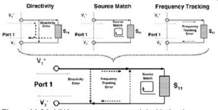
FIG. 31: VNA one-port error model with the three error constants are
computed during calibration to deliver accurate one port measurements
up to measurement plane.
(Adapted from the HP 8510 VNA User's Manual.)
Directivity Error.
Directivity error occurs when less than 100% of the incident signal from the VNA reaches the DUT. This is due primarily to leakage through the test set and reflections due to imperfect adapters. This creates measurement distortion due to the vector sum of the directivity signal combining with the reflected signal from the unknown DUT.
Frequency Tracking Error.
Frequency-response tracking error, sometimes referred to as reflection tracking error, is when there is a variation in magnitude and phase versus frequency between the test and reference signal paths. This is due to differences in length and loss between incident and test signal paths and imperfectly matched samplers.
Source Match Error.
Source match error is due to a reflection between the source and DUT. Since the VNA source impedance is never exactly the same as the load being tested, some of the reflected signal is bounced back down the line, adding with the incident signal. This causes the incident signal magnitude and phase to vary as a function of frequency.
Two-Port Errors.
Two-port measurements compute the transmission coeffi cients of a two-port device by taking the ratio of incident signal and transmitted signal. Two-port measurements S12 and S21 are often referred to as forward and reverse transmission. Sources of error are similar to the one-port described previously, with the addition of isolation and load match. Load match is similar to source match error except under two-port conditions. This refers to the impedance match between the transmission port and DUT. Reflections due to the mismatch between DUT and port 2 may be re-reflected back to port 1, which can cause error in S21. Isolation error is due to the incident signal arriving at the receiver without actually passing through the DUT through an alternative path.
8.6. Calibration for One-Port Measurements
Extracting the previously described error constants versus frequency can eliminate these sources of VNA error. One-port error constants are calculated by measuring open, short, and load at the measurement plane (probe tip). This is completed using a calibration substrate that is matched to the probe type. The calibration substrate is made up of different structures that are designed to interface with the probe tip being used and have highly accurate electrical characteristics. The substrate is used to provide the accurate open, short, and load needed for extremely accurate measurements. The load is usually a laser-trimmed resistive component that is equal to the system impedance desired (usually 50 ohm ). Many substrates include documentation that provides the electrical values to be entered into the VNA for each type of termination. This is done so that when the calibration is performed, the VNA can calculate the proper error constants. An example of a calibration substrate is shown in FIG. 32 along with the various different load types.
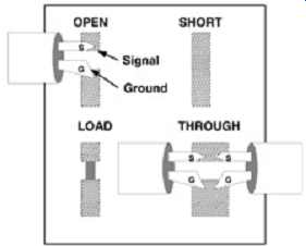
FIG. 32: Typical microprobe calibration substrate with the open, load,
short and thru terminations.
It should be noted that the VNA source match error could still be an issue for cases when the calibration impedance is different from the DUT impedance being measured. Under these circumstances, custom-made substrates to calibrate the impedance of the VNA to the nominal impedance of the DUT can be manufactured.
8.7. Calibration for Two-Port Measurements
Two-port calibrations follow a process similar to that for the one-port, with the addition of one or more through-line test structures (a transmission line of the desired impedance) used to calibrate the S12 and S21 transmission coefficients.
8.8. Calibration Verification
After the calibration procedures have been completed, it is very important to ensure that calibration has been performed correctly. To verify the one-port calibration, the user should measure the substrate and compare the values across the frequency range. With the VNA format in Smith chart format, the user can read the values of the open, short, and load. The values should be as expected for the given measurement setup (the load should be at 1, the open should be at the right-hand side, and the short should be at the left-hand side of the Smith chart, as depicted in FIG. 27). The two-port verification on the through test structures should be completed as well, to verify that the noise floor and propagation delay measurements match the expected value. Once the calibration has been verified to within the accuracy required, the measurements can begin.
Prev. ------- Next