AMAZON multi-meters discounts AMAZON oscilloscope discounts
OVERVIEW
So far, we have covered the fundamental aspects of designing a digital system, ranging from fundamental transmission line theory to design methodologies. After the design is finished and the prototype products have been received, it is necessary to validate the design.
Design validation is necessary to prove that the design is robust, to ensure that no critical aspect of the design was neglected, and to verify that the simulations were accurate enough to predict system performance. Since each particular design is unique and requires specific validation methodologies and equipment based on its functionality and bandwidth, it is difficult to provide a general recipe that steps the engineer through validation. Subsequently, we will not concentrate on a general validation methodology, but instead, on a few aspects of high-speed measurements that will be useful in the validation of virtually any high-speed digital system.
In high-speed digital design and technology development, proper measurement techniques are critical to ensure accurate assessment of system timing margin during design validation and to verify that the simulations correlate with laboratory measurements. Measurements in many ways are the link between simulation and reality and are key to aiding the development process as a check and balance to ensure a robust design. As system speeds increase, the ease of capturing accurate repeatable measurements is becoming increasingly difficult to achieve. Often in modern high-speed designs, the setup and hold margins are only a few hundred picoseconds. To resolve this margin properly and verify the system timings, it is necessary to measure the system to a resolution of approximately one-tenth of the available margin. Subsequently, both the equipment and the measurement techniques must be sufficient or it will become impossible to fully characterize a design in the laboratory.
This Section is intended to give the reader a good understanding of the basic types of equipment available and various measurement techniques that can be used to help extract the critical electrical characteristics for model correlation as well as system validation.
1. DIGITAL OSCILLOSCOPES
Today, the most prominent basic tool for electrical analysis is the digital oscilloscope. The instrument operates by waiting for a trigger event and then recording voltage and time information after the trigger event. Typically, the trigger event is a rising or falling voltage transition past a specified voltage. The instrument typically operates in real-time and/or equivalent-time mode. In real-time operation, the instrument takes consecutive samples of the voltage waveform after the trigger event and constructs the signal accordingly. If the sample rate is not sufficiently fast, the waveform will not be constructed accurately. The sample rate of the instrument strongly affects the quality of the reconstructed waveform in real-time operation. In equivalent-time operation, the instrument assumes that a periodic waveform is under measurement and constructs a displayed waveform from samples taken at varying delays from different triggering events. Basically, in this mode the waveform is constructed as a combination of different periods of the periodic waveform. Real-time and equivalent-time operation are explained further later in this Section. The analog bandwidth of the instrument also affects the quality of the reconstructed waveform. The analog bandwidth gives information on how high frequencies are attenuated when entering the instrument. The bandwidth typically reported for an oscilloscope is the frequency at which the input will be attenuated by 3 dB. If the bandwidth of the oscilloscope is not sufficiently high to capture all significant frequency components of a signal, the measured waveform will not be constructed accurately.
1.1. Bandwidth
The input bandwidth to a scope is similar to an RC circuit, where the R and the C represent the input capacitance and impedance. Subsequently, as derived in Appendix C, the frequency spectrum of an edge passing through an RC circuit is related to the subsequent rise or fall time by equation (1). The rise time in equation (1) is the fastest rise time that can be passed without distortion, assuming the corresponding bandwidth. Since spectral content and rise or fall time are related to each other as shown in equation (1), it is easy to see that the input bandwidth of the scope can filter out high-frequency components of the signal rise time and degrade the signal edge. For example, if the system rise time is 100 ps but the bandwidth of the probe is 2.5 GHz and the input to the scope is 1.5 GHz, the rise time constructed by the oscilloscope will be 290 ps as calculated using the root mean square, as shown in equation (2). The terms Tscope and Tprobe in equation (2) are the rise and fall times calculated with equation (1) from the respective bandwidths of the scope and probe. Equation (1) is valid for rise and fall times measured between 10 and 90% of the amplitude. For different definitions of the rise and fall times (i.e., 20 to 80%), different equations will result.
(1)
(2)
…where Tmeasured is the rise or fall time measured by the scope, Tscope and Tprobe are the minimum rise and fall times that the input of the scope or probe will pass as solved by equation (1), and Tsignal is the actual edge rate.
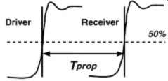
FIG. 1: Illustrative example of flight time (Tprop) showing flight time
as function of voltage threshold.
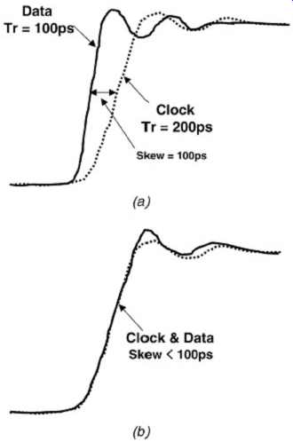
FIG. 2: Example of oscilloscope bandwidth limiting resulting in an error
of measured clock to data skew. (a) actual signals; (b) measured on oscilloscope.
As illustrated in FIG. 1, the time interval measurement (i.e., flight time) is a function of voltage because the measurement is taken at or near the threshold voltage of the receiving buffers (for this case the 50% amplitude point). The key item to understand is that if the scope degrades the signal rise time significantly, flight times and flight-time skews will not be characterized accurately. For example, if two signals exhibit a 100-ps variation in threshold crossing that is caused by a difference in edge rates and the scope used to measure the variation exhibits a bandwidth that is not sufficient to resolve this edge difference, the measured skew would be less. This is demonstrated in FIG. 2. It is important that the input bandwidth of the oscilloscope and the probe be sufficient to measure the edge rates and the skews to sufficient resolution. Another source of measurement error due to inadequate scope bandwidth is the loss of high-frequency aberrations which will be attenuated. It is important to note that sampling, discussed next, will also play a critical role.
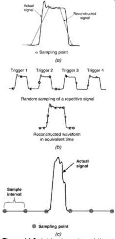
FIG. 3: (a) Inadequate real-time sampling. (b) A random delayed trigger
of a repetitive signal can be used to reconstruct the waveform in equivalent
time. (c) A voltage glitch can be missed altogether if the maximum sampling
rate is wider than the glitch.
1.2. Sampling
A critical parameter in scope performance is sampling method and sample rate. Sampling refers to how the scope captures the data being measured. Digital scopes measure voltages at specific time intervals. These measurements are then reconstructed on the screen. If the time interval between voltage samples is small enough, the result will be an accurate representation of the waveform. Sampling rate refers to the time interval between samples.
For example, if a scope has a sampling rate of 10 gigasamples per second, it means that a sample will be taken every 100 ps.
General oscilloscopes come in two different types of sampling, real time and equivalent time.
Most high-speed designs require real-time sampling for capture of nonperiodic or nonrepetitive (random) events. Real-time sampling refers to a signal that is captured by reconstructing the sample points over a single time interval. That is, the scope will take consecutive voltage samples, following a trigger event, and connect the dots to reconstruct the waveform. The samples used to construct the waveform are taken and displayed in the same sequence as they actually occurred on the signal, hence the name: real-time. If the sample rate is sufficient, the waveform will be represented properly. However, if it is not, the signal shape will not reflect reality. FIG. 3a depicts the effect of an inadequate sample rate in real-time mode.
When real-time sampling is not sufficient to capture the waveform, equivalent-time sampling can sometimes be used. Equivalent-time sampling generates the waveform by piecing together samples from different periods of a periodic waveform. The sample points are taken at slightly different time intervals so that enough points can be sampled to reconstruct the waveform adequately. The input signal is required to be periodic for equivalent-time sampling. The equivalent sample time interval is much smaller allowing for potentially much more accurate reconstruction of periodic waveforms. To accomplish this task, a delayed trigger is used in either sequential or random order. For sequential sampling the trigger delay is a fixed amount. This reconstructs the waveform by capturing different points along the waveform in time until enough points are stored to reproduce the waveform accurately.
Random repetitive sampling is similar to sequential except that sampling is completed randomly versus a fixed delay trigger. An example of equivalent-time sampling is illustrated in FIG. 3b.
It should be noted that equivalent-time sampling is only sufficient to capture repetitive events.
To capture random or nonperiodic events, it is necessary to use real-time sampling. This causes a problem in high-speed measurements. Equivalent time will average out nonperiodic events, and real time may not capture them if the sample rate is not high enough. As illustrated in FIG. 3c for nonperiodic waveform capture, the real-time sampling rate can determine whether a glitch is captured at all. Random glitches in the signals can cause system failures. If the sample rate is not sufficient, it becomes extremely difficult to capture these random events. In cases where the width of the glitch is less than the sampling rate, signal capture may be missed altogether. Similarly, in FIG. 4, the actual placement of the edge can be unknown if a sample does not fall on the transition.
FIG. 5 shows another example of lost information due to inadequate sample rate.
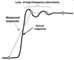
FIG. 4: How measurement resolution loss occurs when the sampling rate
is inadequate.
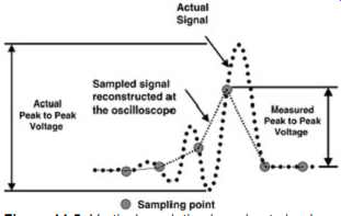
FIG. 5: Vertical resolution loss due to inadequate sampling of high-frequency
signal.
1.3. Other Effects
There are many other effects of the measurement equipment that can affect measurement accuracy. Although a detailed account of each of these effects is beyond the scope of this book, some of them are mentioned here briefly.
Internal Oscillator Accuracy and Stability.
The timing reference points inside the oscilloscope are typically based off a crystal oscillator.
The quality of the crystal chosen by the manufacturer will affect the accuracy and frequency stability of the instrument. The oscillator will have a nominal accuracy and will also change slightly with time. Oscilloscopes tend to be far more accurate with relative time measurements (such as comparing the edge rates of similar signals) than with absolute time measurements (such as measuring a long period very accurately). With relative time measurements, the nominal accuracy may not matter. However, since the frequency accuracy of the internal oscillator can vary with time, relative measurements separated over long lengths of time may yield inaccurate results. The oscillator may also have temperature sensitivities and other imperfections.
Analog-to-Digital Converter Resolution.
The voltage amplitude has a finite resolution due to the analog-to-digital converter used internally. Most oscilloscopes use an 8-bit analog-to-digital converter which allows a granularity of 256 levels of amplitude. Typically, the 256 levels are scaled to the display.
Thus, at any time the fraction of the display used is the fraction of the analog-to-digital converter that is being used. Thus, for accurate amplitude measurements, the waveform should be scaled to fill a good fraction of the display.
Trigger Jitter.
This is the variation in placement of the trigger by the instrument. This can lead to apparent time variation of a measurement.
Interpolation.
How the instrument chooses to "connect the dots" can affect the shape of a reconstructed waveform. Various interpolation algorithms exist and are usually selectable. The user may also choose to shut off interpolation and see only the captured points.
Aliasing.
In certain measurements, effects can be observed which are a result of sampling a frequency or frequency component at a sampling rate less than required to capture the signal. This can sometimes result in apparent lower-frequency components that do not actually exist in the signal. Mathematically, to capture a frequency component, you must sample at a minimum rate of twice the frequency of interest. For practical instruments, it is typically assumed that you must sample at four times the maximum frequency of interest.
This is why the maximum sample rate of an oscilloscope that is to be used for real-time sampling is typically four times its rated analog bandwidth. Aliasing is most pronounced at sample rates less than maximum.
1.4. Statistics
Statistics are necessary to indicate measurement repeatability and reproducibility for systems that include significant jitter, which is variation in a measurement. Jitter is so named because when observed on the screen the waveform will appear to shake or blur if jitter is present. By utilizing some basic statistical parameters, one can check to see if the particular measurement is stable. Measurement stability can be verified by taking a number of samples and computing the mean and standard deviation from the Gaussian distribution. This is a function on many modern oscilloscopes. This should be completed on any new measurement setup to verify that measured differences in the results are not within the noise of the measurement. FIG. 6 illustrates an example of a Gaussian distribution of a rise time measurement. Because jitter exists in the system, the edge rate may be changing, which could make it difficult to produce repeatable results. By measuring the mean and standard deviation for a parameter such as rise time, one can compute more accurate and repeatable results in the presence of jitter effects by computing the rise time from the statistical means at the two measurement points (i.e., 10% and 90%).
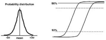
FIG. 6: The probability distribution can be used to incorporate the effects
of jitter on rise time.
2. TIME-DOMAIN REFLECTOMETRY
In previous Sections we saw how the waveform at a driver is determined by reflected components. Time-domain reflectometery (TDR) refers to measuring a system by injecting a signal and observing the reflections. Typically, a step function with a defined transition time is driven into a transmission line and the waveform at the driver is observed. Thus, the features of all the downstream reflection effects on the driver end of the line, such as ledges, overshoot, and undershoot, can be observed and back-calculated to characterize the impedance discontinuities on the transmission line. A similar method which looks at transmitted waves rather then reflected waves, called a TDT (time-domain transmission), is explained later in the Section.
At high speeds, the interconnect can be the major factor in limiting system performance. To predict performance early in the design phase, it is extremely important to characterize and model the interconnect accurately. Time-domain reflectometry (TDR) measurements are common for PCB board characterization. The key advantage of the TDR over frequency domain measurements is the ability to extract electrical data relevant to digital systems, which represent time-domain signals. As mentioned in previous Sections, digital signals represent wide bandwidth signals, not single frequencies as prominent in typical microwave designs. Extracting data in the time domain provides voltage-time data that relate back to system operation. By utilizing the TDR, one can extract impedance, velocity, and mutual and self-transmission line electrical parameters. In the following section we discuss the basic theory and operation of the TDR to extract interconnect electrical characteristics.
2.1. TDR Theory
The TDR uses basic transmission line theory by measuring the reflection of an unknown device relative to a known standard impedance. This is based on knowing that energy transmitted through any discontinuity will result in energy being reflected back. The reflection magnitude will be a function of both the transmitted energy and the magnitude of the impedance discontinuity. The time delay between transmitted and reflected energy will be a function of distance and propagation velocity.
Impedance information is extracted by calculating the reflection coefficient, ohm, as a function of the incident and reflected voltages. Using the TDR reference characteristic impedance and ohm, the trace characteristic impedance can be computed using the equations
(3)
(4)
The equations above can be used to calculate the trace impedance (ZDUT) [device under test (DUT)], where Zo represents the output impedance of the TDR. The oscilloscope will calculate the value of omega to determine the trace impedance.
The simplified generic example of a TDR driver output and receiver is illustrated in FIG. 7. This contains a step generator, sampler, and reference 50-ohm termination. This illustration exemplifies a current source output stage. It should be noted that the output could be a voltage source as well, with a series Thévenin resistance. The sampler represents the receiver and is used to capture the reflected response as an input to the oscilloscope.
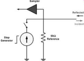
FIG. 7: Simplified example of a current-source TDR output stage, including
sampling input to oscilloscope.
So now that the basic theory and operation of the TDR has been covered in the following section we go through some representative examples of extracting the basic impedance and velocity characteristics. In most practical situations the instrument TDR output is connected to a 50-ohm cable. Launching a pulse into a known cable of 50 ohm yields an incident wave with an amplitude of V, due to the resistive divider effect between the cable and the 50-ohm source resistance. The waveform reflected from the load is delayed by two electrical lengths and is superimposed back at the TDR output.
An example of a TDR response, including the cable and terminated trace (DUT), is illustrated in FIG. 8. For this case the cable, which is assumed to be an ideal 50 ohm, is connected to a 60-ohm trace that is terminated with a 60-ohm resistor. The respective ideal TDR response shows the incident and reflected voltages used to calculate ZDUT. This also shows the round-trip delay, Td, for the overall system as well as for each individual section.
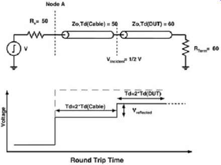
FIG. 8: Basic example of TDR response as seen at node A for test conditions.
The response illustrates the voltage and time relationship as the pulse
propagates to termination.
Another example is shown in FIG. 9. This illustrates the effect of high- and low impedance discontinuities along a 50-ohm trace. For the capacitive discontinuity loading case, the voltage decreases, and in the inductive discontinuity case, the voltage increases. FIG. 10 represents lumped-element discontinuities. The lumped responses shown in FIG. 10 illustrate the inductive and capacitive response for small discontinuities such as vias and PCB trace bends.
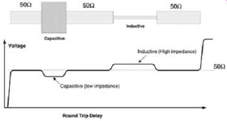
FIG. 9: Simplified response illustrating the TDR response effect to capacitive
and inductive loading along a 50-ohm line.
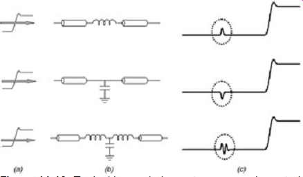
FIG. 10: Typical lumped element response characteristics: (a) TDR input;
(b) lumped element; and (c) response.
2.2. Measurement Factors
To properly characterize and interpret TDR response characteristics as related to the DUT (device under test), the real-life factors that affect TDR resolution in the laboratory must be understood. Insufficient resolution will produce misleading results that can miss details of impedance and velocity profiles. This is common when items to be measured are very closely spaced or when the impedance discontinuities are electrically very short. The major resolution factors for TDR are rise time, settling time, foot, and pre-shoot, as illustrated in FIG. 11.
FIG. 11: TDR pulse characteristics that affect measurement resolution. Rise Time.
The most prominent TDR characteristic that affects resolution is the pulse rise time. As discussed previously, the response is based on the reflection. The general rule of thumb is that the reflection from two narrowly spaced discontinuities will be indistinguishable if they are separated by less than half the rise time. Subsequently, the TDR can only accurately resolve structures that are electrically long compared to the rise time.
(5)
System rise (Trise) time is characterized by the fall or rise time of the reflected edge from an ideal short or open at the probe tip.
Faster rise times usually provide more versatility for analyzing small electrical parasitics but are also harder to interpret correctly. Most systems designs may operate at a much slower edge rate than the TDR output. Subsequently, the peaks and dips of the impedance discontinues measured with a TDR will not necessarily represent those seen in the system because the slower edge rate will tend to mask small variations. For example, consider two microstrip PCB traces from two different boards that are connected together with a typical inductive connector. The connector is soldered to the main board, while the second board fits into the connector similar to a PCI or ISA card. The ISA or PCI board has pads called edge fingers that are exposed and fit in the connector to make electrical contact. To characterize the connector between the two boards, the overall lumped electrical model must include the connector, via, and the edge finger pad capacitance as illustrated in FIG. 12. FIG. 13 shows the respective TDR response of the connector for different edge rates. Notice how the effect of the inductive impedance discontinuity decreases with slow edge rates. The effect of edge rates on reflections is explained in Section 2.4.3.
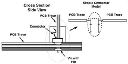
FIG. 12: Cross-section view of two different PCB boards connected by
a typical connector along with the simple model.
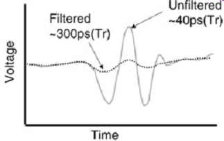
FIG. 13: The TDR response for two different edge rates illustrates the
resolution difference on the connector lumped elements. Incident Characteristics.
The inherent TDR response characteristics, such as settling time, foot, and preshoot (see FIG. 11), are also important to consider with respect to TDR resolution. The incident response characteristics are essentially the difference between the ideal and actual step response. The foot and preshoot refer to the section of the response prior to the vertical edge, while settling time is the time for the response to settle.
These characteristics are inherent in the incident wave and will affect the resolution of the measurement. A simple example of this can be illustrated with the settling time. If the settling time is long compared to the electrical delay of the structure being measured, it may induce false readings because the impedance measurement might be taken at a peak or dip in the response. This would look like an impedance variation when in reality it is simple inherent ringing in the response. Possible methods to minimize these effects are covered in the following section.
3. TDR ACCURACY
TDR accuracy depends on two main components: equipment-related issues and the test system. The equipment issues include items such as step generator and sampler imperfections that are controlled by the TDR manufacturer. The test system refers to the measurement setup that incorporates cabling, probes, and type of DUT to be tested. Launch parasitics, cable losses, multiple reflections, and interface transmission loss are all factors that can affect TDR accuracy.
For the purposes of this section, only the test system is covered, as the end user has minor control over the equipment's accuracy factors. In most cases the test system is the most critical factor in taking accurate TDR measurements. As discussed earlier, the TDR extracts impedance information based on the voltage response in time. Under ideal conditions, the response is flat during the time of interest. In the real lab environment, the response may not be so flat and could therefore affect the accuracy of the measurement. These nonideal effects along the TDR response are referred to as aberrations.
In some cases, aberrations can be a significant percentage of the total response.
Aberrations due to the preshoot and foot of the response can be predictable. Predictable responses can use processing techniques with software to account for these effects.
Unpredictable responses due to ringing and multiple reflections are not accountable. An example where the response is predictable is illustrated in FIG. 14. TDR pulse response exhibits the foot, preshoot, and settling effects. These characteristics are also replicated in the reflected portion of the response. Therefore, since the incident response characteristics will be replicated in the reflected response, the possibility of utilizing software or digital signal processing within the TDR could be used to help eliminate some inaccuracies due to the predictable incident characteristics.
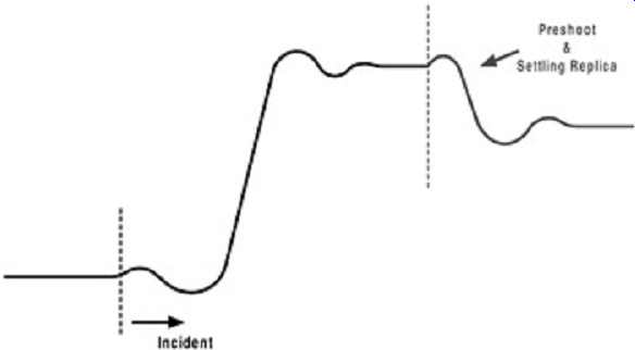
FIG. 14: Example of how the incident pulse characteristics will be replicated.
3.1. Launch Parasitics
One cause of unpredictable response characteristics is launch parasitics. Launch parasitics cause aberrations in the step response that can be unpredictable and therefore may not be repeatable. The goal of launching a fast edge while maintaining signal integrity is largely affected by reliable physical connection to the DUT, probe ground-loop inductance, and structure crosstalk. Ground-loop inductance effects due to the probe type used as an interface between the DUT and TDR are critical. Large impedance discontinuities between the TDR instrument and DUT will cause significant aberrations in the TDR response.
Increasing the ground loop of the probe increases the effective inductive discontinuity between the instrument and the DUT. The larger the discontinuity, the larger aberrations that will be seen in the response, which leads to decreased accuracy.
FIG. 15 illustrates two different examples of common hand-held probes with varying ground loops that are dependent on the probe grounding mechanism, called the ground spanner. It is can be seen that the probe with the long spanner will have a larger ground loop than the probe type with the small ground spanner. The larger ground loop probe will exhibit a higher-impedance discontinuity, due to the ground return path, which will make the probe response look inductive. The smaller ground-loop probe will have an inductive effect that is much smaller in magnitude than the large ground-loop probe.
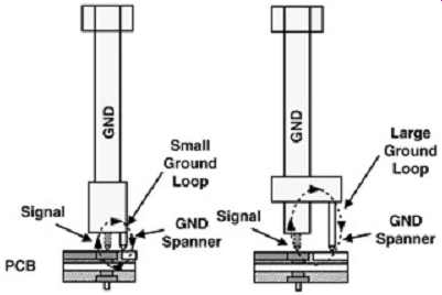
FIG. 15: Examples of different hand-held type probes with varying ground
loops.
FIG. 16 shows the various response characteristics for different types of probes with varying ground-loop effects. It shows the importance of being able to control the discontinuity by minimizing the ground loop. Improved TDR response characteristics will be achieved with probe types that minimize the discontinuity between the instrument and the DUT. It should also be noted that the large ground loops tend to degrade the TDR edge. This will have a negative effect on the accuracy of the impedance and delay measurements. Minimizing the probe ground loop will generally improve settling time and minimize edge rate degradation, thereby increasing the resolution of the measurement.
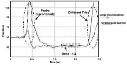
FIG. 16: This illustrates a typical TDR response difference between two
different handheld probes with different ground loops.
3.2. Probe Types
The most commonly used probes in use today are the hand-held, surface-mounted adapter (SMA) and the microprobe. The primary factors that need to be considered when choosing the probe are accuracy and the amount of work involved to complete the measurements.
The difference between probes will play a critical role in accuracy and repeatability.
The probe's purpose is to provide a connection between the measurement equipment and the DUT. Anytime the probe is not exactly 50 ohm, an impedance discontinuity will occur between the TDR output and the load under test. This discontinuity will cause a reflection at the probe and decrease the accuracy of the measurements. Minimizing this reflection requires that the probe exhibit a continuous impedance of 50 ohm all the way to the probe tip (because it matches the cable and the output impedance of the equipment). The impedance mismatch between the cable and the probe is one of the primary factors that affect measurement accuracy. The smaller the discontinuity, the greater the accuracy [McCall, 1999].
The most commonly used probe type is the hand-held probe. This probe is useful for quick checks but is not adequate for the most accurate or repeatable measurements. A common problem with hand-held probing is measurement error due to the ground connection mechanism of the probe (the ground spanner). Selecting the proper ground spanner is critical to minimizing the discontinuity, due to the probe ground-loop inductance. Minimizing the ground-loop inductance reduces the initial spike (high impedance) as the pulse launches into the load under test. The benefits of minimizing the ground loop are improved settling time, response smoothness, and decreased probe loss.
SMA connectors soldered to the board will provide good repeatability because they are soldered onto the board. The problem is that they tend to exhibit rather high capacitive loading, which reduces the effective edge rate of the TDR pulse into the device under test.
SMA connectors are not good for measurement conditions that need to utilize maximum resolution of TDR instruments [McCall, 1999].
Controlled impedance microprobes are the most accurate probe type that can be used.
Microprobes exhibit very small parasitics, very small ground loops, and are usually 50 ohm all the way to the probe tip (although high-impedance microprobes can also be purchased). Microprobes are generally used for characterizing radio-frequency and microwave circuits.
These are predominately used in the industry with the vector network analyzer (VNA), which is explained later in this Section. However, in the digital world they can be used for the most accurate TDR measurements. The major disadvantage of these probes is that they require a probe station, special probe holders, and a microscope.
_3.3. Reflections
Multiple reflections in the test system may or may not be predictable. Remember that the TDR response is a reflection profile, not an impedance profile. Also remember that reflection magnitude and the resolution will be a factor of rise-time degradation. If the resolution is lost, the predictability of reflections will also be lost. The most accurate line measurements are usually completed on lines that have no discontinuity, such as impedance coupons. A good rule of thumb is to minimize reflections prior to the DUT and any impedance discontinuities between the TDR and DUT. This requires the engineer to use a controlled-impedance, low loss cable as the interface between the TDR and the probe. Furthermore, a low-loop inductance, controlled-impedance probe is required. To understand the effect of multiple reflections due to multiple impedance discontinuities, one can apply a lattice diagram. This is shown in FIG. 17, illustrating the superposition of reflections for multiple impedance discontinuities.
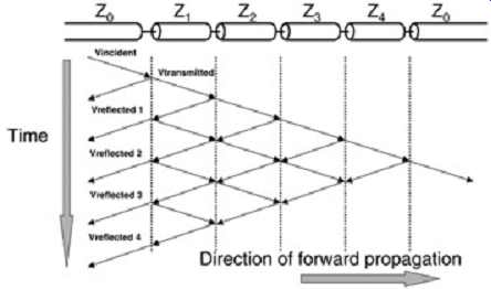
FIG. 17: Lattice diagram of multiple discontinuities, resulting in the
superposition of reflections.
3.4. Interface Transmission Loss
Interface transmission loss is a big factor, especially in test system environments that are significantly different than the instrument 50 ohm reference. When the test system impedance is significantly different from the DUT, only a portion of the initial energy-launched into the interface is transmitted. Therefore, a reflection with a smaller amplitude is passed back through the interface to the source. This will make it difficult to measure impedance's significantly different than 50 ohm .
3.5. Cable Loss
Most test systems will have a cable interface between the instrument and the probe. Cable loss is another factor that can reduce accuracy, by causing apparent shifts in characteristic impedance. This is due primarily to skin effect losses, which create a pseudo-dc shift in the line impedance. Amplitude degradation will occur as the pulse propagates down a lossy line, resulting in an error between the actual incident amplitude input versus the output of a cable.
This inaccuracy can either be eliminated by the use of expensive low-loss cables or compensated following the proper measurement techniques that will be covered later in the TDR accuracy improvement sections.
3.6. Amplitude Offset Error
Amplitude offset error is when the incident voltage amplitude varies versus the reference voltage. A common effect that is noticed on some TDR measurements is a reading variation, depending on whether or not the DUT is terminated. If the impedance of a cable, for example, is measured, the reading may change, depending on whether the cable is left open or is terminated. It is possible that the reading could exhibit a 1- or 2-ohm delta between the open-ended and terminated case. This is a result of providing a dc path to ground that simply loads the step generator driver, causing a reduction in the incident step amplitude. To eliminate the source of error for general impedance measurements, it is always recommended to leave the DUT open ended.
4. IMPEDANCE MEASUREMENT
The following procedures will aid the engineer to account for the major sources of TDR inaccuracy, resulting in very accurate impedance measurements [IPC-2141, 1996]. These measurements utilize a reference standard airline or golden standard, of which the impedance and delay has been carefully characterized. It is possible to purchase airline standards that are NIST (National Institute of Standards Test) certified to achieve the greatest accuracy to less than 0.1 ohm. To achieve the most accurate results, the impedance of the reference standard should be very close to the test system characteristic impedance to minimize interface transmission losses. For example, if the test system environment design was nominal 30 ohm, a reference standard with the same impedance should be chosen.
FIG. 18 shows the basic test setup. This includes the cable, probe, DUT, and airline standard. Both the airline standard and the DUT must be open ended. The probe type, for the purpose of this example, should have a controlled impedance that matches the cable and should exhibit very small parasitics.
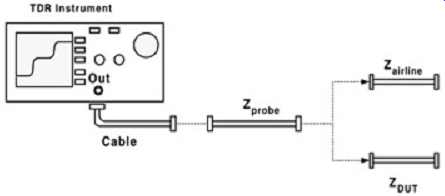
FIG. 18: Basic test setup for accurate impedance measurements using an
airline reference standard.
4.1. Accurate Characterization of Impedance
As described above, there are several sources of error that will decrease the accuracy of an impedance measurement. Described below are two different ways of measuring the impedance accurately and negating some of these errors.
Back Calculation Using the Standard Reference.
The first step is to determine the probe impedance. This is determined by measuring the step size of the incident response at the probe tip. This is done with the open-ended probe attached to the end of the cable as shown in FIG. 18. Next, the airline is connected to the cable, and the reflected step response is measured as shown in FIG. 19. The probe impedance can be calculated by using the equation (6)…
…where VI is the incident step response, VR the reflected step response, and Zairline the known impedance of the standard airline.
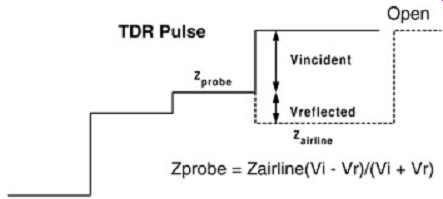
FIG. 19: Measurement response for determining Zprobe.
Now that the probe impedance is determined, we can calculate the actual DUT impedance by following a similar procedure. Measure the incident step size with the probe open and then measure the reflected step response while probing the DUT. The DUT characteristic impedance is extracted using the equation (7).
In many cases the discontinuity of the probe being used is too small to determine the impedance. Completing the same measurement as discussed previously using the cable as the reference instead of the probe can provide good results, on the order of less than 1-ohm difference. This is especially true in cases where the probe impedance effects are quite small.
Offset Method.
Another technique of measuring impedance is the offset method. The offset method simply uses a fixed value that accounts for the difference between the standard and the actual readings. A standard characterized impedance reference (such as the airline) is measured and the difference between the measurement and the known impedance is the offset. When measuring the DUT, the offset is applied to the measurement result to account for errors.
This technique is especially useful for inexperienced users. This assumes a linear relationship within the given specification window which is not necessarily correct. Although inferior to the back-calculation method, it does produce relatively accurate results with less time.
Impedance Coupon.
Depending on the topology of the bus design, it may or may not be possible to measure the actual signal traces to determine the bus characteristic impedance. This will depend on the length of the traces and bus impedance. The larger the difference in Zo between the DUT and TDR, the longer the settling time to obtain a flat response. Furthermore, it may not be possible to probe the signal traces on the final board design without using a probe with a large inductive ground loop. To circumvent this problem, an impedance coupon can be used.
In PCB manufacturing, impedance coupons are used to dial in the process to obtain the target impedance. To characterize the characteristic impedance, it is important that the coupon geometry replicates the bus design. It is also critical that the coupon is designed properly for obtaining accurate measurements.
4.2. Measurement Region in TDR Impedance Profile
Measurement methodology can play a big role in correlation and accuracy. For example, the TDR response in FIG. 20 illustrates measurement of a 6-in. low-impedance coupon using a common hand-held type of probe. Notice the initial inductive spike and the amount of time it takes the response to settle. The purpose of this illustration is to show the possible variations in the results due to cursor positioning along the response. Measurements that are taken during the settling time will contain more variability and will therefore be prone to incorrect readings. To minimize the variability of measurement location along the response, a good rule of thumb is to measure the mean of the response along the flattest region, as highlighted in FIG. 20. This works well provided that the structure is long enough to allow for sufficient settling time.
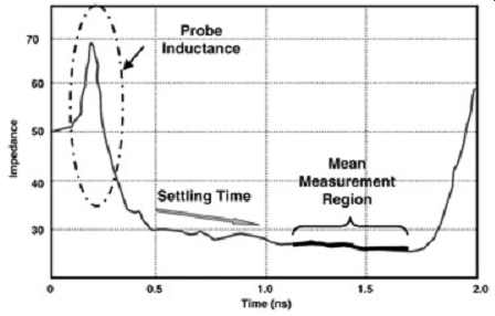
FIG. 20: Measurement of low impedance 6 in. microstrip coupon with an
inductive probe.
The second item to note is that trying to measure a short trace would lead to incorrect impedance values because there is insufficient time for the response to settle. In the case of FIG. 20, the measurement of the 6-in. trace takes several hundreds picoseconds to settle. If an identical 1-in. trace, for example, was characterized, the ringing from the inductive probe would not have time to settle before the reflection from the open at the end of the trace returns to the sample head. Subsequently, there would be no flat areas of the response to measure, and it would be very difficult to achieve accurate results. This is a common error made in today's industry. As mentioned previously, proper coupon design is also critical for accurate impedance measurements. Test coupons should be designed to replicate the bus design and therefore should take into account trace geometry, copper density, and location on the PCB.
RULES OF THUMB: Obtaining Accurate Impedance Measurements with a TDR
---Complete measurements with the DUT open circuited. This eliminates step amplitude variation due to dc loading.
---Obtain measured data in the flattest region of the TDR response. This should be far away from the incident step, where aberrations will be most pronounced.
---Try to minimize probe discontinuities and cable loss. Use of small, controlled impedance microprobes along with low-loss cables will minimize these sources of error.
---Utilize test structures that are long enough to allow the TDR signal to settle.
---When designing an impedance coupon, try to replicate the topologies that will be used in the design.