AMAZON multi-meters discounts AMAZON oscilloscope discounts
Radio-frequency (RF) electronics differ from other electronics because the higher frequencies make some circuit operation a little hard to understand. Stray capacitance and stray inductance afflict these circuits. Stray capacitance is the capacitance that exists between conductors of the circuit, between conductors or components and ground, or between components. Stray inductance is the normal inductance of the conductors that connect components, as well as internal component inductances. These stray parameters are not usually important at dc and low ac frequencies, but as the frequency increases, they become a much larger proportion of the total. In some older very high frequency (VHF) TV tuners and VHF communications receiver front ends, the stray capacitances were sufficiently large to tune the circuits, so no actual discrete tuning capacitors were needed.
Also, skin effect exists at RF. The term skin effect refers to the fact that ac flows only on the outside portion of the conductor, while dc flows through the entire conductor. As frequency increases, skin effect produces a smaller zone of conduction and a correspondingly higher value of ac resistance compared with dc resistance.
Another problem with RF circuits is that the signals find it easier to radiate both from the circuit and within the circuit. Thus, coupling effects between elements of the circuit, between the circuit and its environment, and from the environment to the circuit become a lot more critical at RF. Interference and other strange effects are found at RF that are missing in dc circuits and are negligible in most low frequency ac circuits.
The electromagnetic spectrum
When an RF electrical signal radiates, it becomes an electromagnetic wave that includes not only radio signals, but also infrared, visible light, ultraviolet light, X-rays, gamma rays, and others. Before proceeding with RF electronic circuits, therefore, take a look at the electromagnetic spectrum.
The electromagnetic spectrum ( FIG. 1) is broken into bands for the sake of convenience and identification. The spectrum extends from the very lowest ac frequencies and continues well past visible light frequencies into the X-ray and gamma ray region. The extremely low frequency (ELF) range includes ac power-line frequencies as well as other low frequencies in the 25- to 100-hertz (Hz) region. The U.S. Navy uses these frequencies for submarine communications.
The very low frequency (VLF) region extends from just above the ELF region, although most authorities peg it to frequencies of 10 to 100 kilohertz (kHz). The low frequency (LF) region runs from 100 to 1000 kHz-or 1 megahertz (MHz). The medium-wave (MW) or medium-frequency (MF) region runs from 1 to 3 MHz. The amplitude-modulated (AM) broadcast band (540 to 1630 kHz) spans portions of the LF and MF bands.
The high-frequency (HF) region, also called the shortwave bands (SW), runs from 3 to 30 MHz. The VHF band starts at 30 MHz and runs to 300 MHz. This region includes the frequency-modulated (FM) broadcast band, public utilities, some television stations, aviation, and amateur radio bands. The ultrahigh frequencies (UHF) run from 300 to 900 MHz and include many of the same services as VHF. The microwave region begins above the UHF region, at 900 or 1000 MHz, depending on source authority.
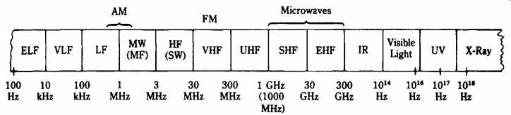
FIG. 1 The electromagnetic spectrum from VLF to X-ray. The RF region covers
from less than 100 kHz to 300 GHz
You might well ask how microwaves differ from other electromagnetic waves.
Microwaves almost become a separate topic in the study of RF circuits because at these frequencies the wavelength approximates the physical size of ordinary electronic components. Thus, components behave differently at microwave frequencies than they do at lower frequencies. At microwave frequencies, a 0.5-W metal film resistor, for example, looks like a complex RLC network with distributed L and C values-and a surprisingly different R value. These tiniest of distributed components have immense significance at microwave frequencies, even though they can be ignored as negligible at lower RFs.
Before examining RF theory, first review some background and fundamentals.
Units and physical constants
In accordance with standard engineering and scientific practice, all units in this book will be in either the CGS (centimeter-gram-second) or MKS (meter kilogram-second) system unless otherwise specified. Because the metric system depends on using multiplying prefixes on the basic units, a table of common metric prefixes ( TBL. 1) is provided. TBL. 2 gives the standard physical units. TBL. 3 gives physical constants of interest in this and other sections. TBL. 4 gives some common conversion factors.
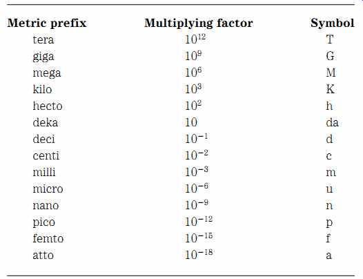
TBL. 1. Metric prefixes
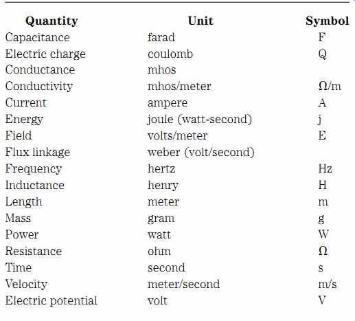
TBL. 2. Units of measure
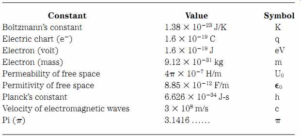
TBL. 3. Physical constants
TBL. 4. Conversion factors
Wavelength and frequency
For all wave forms, the velocity, wavelength, and frequency are related so that the product of frequency and wavelength is equal to the velocity. For radio waves, this relationship can be expressed in the following form:
(Eqn. 1)
...where ...
_ = wavelength in meters (m)
F= frequency in hertz (Hz)
_ dielectric constant of the propagation medium
c = velocity of light (300,000,000 m/s).
The dielectric constant ( ) is a property of the medium in which the wave prop agates. The value of is defined as 1.000 for a perfect vacuum and very nearly 1.0 for dry air (typically 1.006). In most practical applications, the value of in dry air is taken to be 1.000. For media other than air or vacuum, however, the velocity of propagation is slower and the value of _ relative to a vacuum is higher. Teflon, for example, can be made with values from about 2 to 11.
Equation (Eqn. 1) is more commonly expressed in the forms of Eqs. (Eqn. 2) and
(Eqn. 3):
(Eqn. 2) and (Eqn. 3)
[All terms are as defined for Eq. (Eqn. 1).]
Microwave letter bands
During World War II, the U.S. military began using microwaves in radar and other applications. For security reasons, alphabetic letter designations were adopted for each band in the microwave region. Because the letter designations became in grained, they are still used throughout industry and the defense establishment. Un fortunately, some confusion exists because there are at least three systems currently in use: pre-1970 military ( TBL. 5), post-1970 military ( TBL. 6), and the IEEE and industry standard ( TBL. 7). Additional confusion is created because the military and defense industry use both pre- and post-1970 designations simultaneously and industry often uses military rather than IEEE designations. The old military designations ( TBL. 5) persist as a matter of habit.
Skin effect
There are three reasons why ordinary lumped constant electronic components do not work well at microwave frequencies. The first, mentioned earlier in this section, is that component size and lead lengths approximate microwave wavelengths.
==========
TBL. 5. Old U.S. military microwave frequency bands (WWII-1970)
Band designation --- Frequency range
P 225-390 MHz
L 390-1550 MHz
S 1550-3900 MHz
C 3900-6200 MHz
X 6.2-10.9 GHz
K 10.9-36 GHz
Q 36-46 GHz
V 46-56 GHz
Q 56-100 GHz
==========

TBL. 6. New U.S. military microwave frequency bands (Post-1970)
==============

TBL. 7. IEEE/Industry standard frequency bands
=================
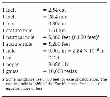
The second is that distributed values of inductance and capacitance become significant at these frequencies. The third is the phenomenon of skin effect. While dc cur rent flows in the entire cross section of the conductor, ac flows in a narrow band near the surface. Current density falls off exponentially from the surface of the conductor toward the center ( FIG. 2). At the critical depth (_, also called the depth of penetration), the current density is 1/e _ 1/2.718 _ 0.368 of the surface current density.
The value of _ is a function of operating frequency, the permeability () of the conductor, and the conductivity ( ). Equation (Eqn. 4) gives the relationship.
(Eqn. 4) where
__ critical depth
F = frequency in hertz
_ permeability in henrys per meter
_ conductivity in mhos per meter.
__ B 1 2_F
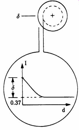
FIG. 2-- In ac circuits, the current flows only in the outer region of the
conductor. This effect is frequency-sensitive and it becomes a serious consideration
at higher RF frequencies.
RF components, layout, and construction
Radio-frequency components and circuits differ from those of other frequencies principally because the unaccounted for "stray" inductance and capacitance forms a significant portion of the entire inductance and capacitance in the circuit. Consider a tuning circuit consisting of a 100-pF capacitor and a 1-uH inductor. According to an equation that you will learn in a subsequent section, this combination should resonate at an RF frequency of about 15.92 MHz. But suppose the circuit is poorly laid out and there is 25 pF of stray capacitance in the circuit. This capacitance could come from the interaction of the capacitor and inductor leads with the chassis or with other components in the circuit. Alternatively, the input capacitance of a transistor or integrated circuit (IC) amplifier can contribute to the total value of the "strays" in the circuit (one popular RF IC lists 7 pF of input capacitance). So, what does this extra 25 pF do to our circuit? It is in parallel with the 100-pF discrete capacitor so it produces a total of 125 pF. Reworking the resonance equation with 125 pF instead of 100 pF reduces the resonant frequency to 14.24 MHz.
A similar situation is seen with stray inductance. All current-carrying conductors exhibit a small inductance. In low-frequency circuits, this inductance is not sufficiently large to cause anyone concern (even in some lower HF band circuits), but as frequencies pass from upper HF to the VHF region, strays become terribly important. At those frequencies, the stray inductance becomes a significant portion of total circuit inductance.
Layout is important in RF circuits because it can reduce the effects of stray capacitance and inductance. A good strategy is to use broad printed circuit tracks at RF, rather than wires, for interconnection. I've seen circuits that worked poorly when wired with #28 Kovar-covered "wire-wrap" wire become quite acceptable when redone on a printed circuit board using broad (which means low-inductance) tracks.
FIG. 3 shows a sample printed circuit board layout for a simple RF amplifier circuit. The key feature in this circuit is the wide printed circuit tracks and short distances. These tactics reduce stray inductance and will make the circuit more predictable.
Although not shown in FIG. 3, the top (components) side of the printed circuit board will be all copper, except for space to allow the components to interface with the bottom-side printed tracks. This layer is called the "ground plane" side of the board.
Impedance matching in RF circuits
In low-frequency circuits, most of the amplifiers are voltage amplifiers. The requirement for these circuits is that the source impedance must be very low com pared with the load impedance. A sensor or signal source might have an output impedance of, for example, 25 ohm. As long as the input impedance of the amplifier receiving that signal is very large relative to 25 ohm, the circuit will function. "Very large" typically means greater than 10 times, although in some cases greater than 100 times is preferred. For the 25-ohm signal source, therefore, even the most stringent case is met by an input impedance of 2500 ohm, which is very far below the typical input impedance of real amplifiers.

FIG. 3 Typical RF printed circuit layout.
RF circuits are a little different. The amplifiers are usually specified in terms of power parameters, even when the power level is very tiny. In most cases, the RF circuit will have some fixed system impedance (50, 75, 300, and 600 ohm being common, with 50 ohm being nearly universal), and all elements of the circuit are expected to match the system impedance. Although a low-frequency amplifier typically has a very high input impedance and very low output impedance, most RF amplifiers will have the same impedance (usually 50 ohm) for both input and output.
Mismatching the system impedance causes problems, including loss of signal--especially where power transfer is the issue (remember, for maximum power transfer, the source and load impedances must be equal). Radio-frequency circuits very often use transformers or impedance-matching networks to affect the match between source and load impedances.
Wiring boards
Radio-frequency projects are best constructed on printed circuit boards that are specially designed for RF circuits. But that ideal is not always possible. Indeed, for many hobbyists or students, it might be impossible, except for the occasional project built from a magazine article or from this book. This section presents a couple of alternatives to the use of printed circuit boards.
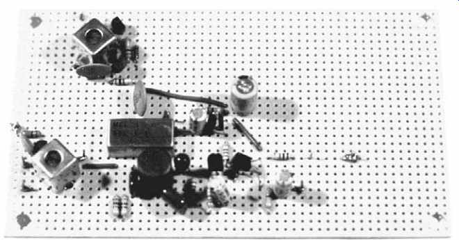
FIG. 4 Perfboard layout.
FIG. 4 shows the use of perforated circuit wiring board (commonly called perfboard). Electronic parts distributors, RadioShack, and other outlets sell various versions of this material. Most commonly available perfboard offers 0.042 holes spaced on 0.100 centers, although other hole sizes and spacings are available. Some perfboard is completely blank, and other stock material is printed with any of several different patterns. The offerings of RadioShack are interesting because several different patterns are available. Some are designed for digital IC applications and others are printed with a pattern of circles, one each around the 0.042 holes.
In FIG. 4, the components are mounted on the top side of an unprinted board.
The wiring underneath is "point-to-point" style. Although not ideal for RF circuits, it will work throughout the HF region of the spectrum and possibly into the low VHF (especially if lead lengths are kept short).
Notice the shielded inductors on the board in FIG. 4. These inductors are slug tuned through a small hole in the top of the inductor. The standard pin pattern for these components does not match the 0.100-hole pattern that is common to perf board. However, if the coils are canted about half a turn from the hole matrix, the pins will fit on the diagonal. The grounding tabs for the shields can be handled in either of two ways. First, bend them 90 degrees from the shield body and let them lay on the top side of the perfboard. Small wires can then be soldered to the tabs and passed through a nearby hole to the underside circuitry. Second, drill a pair of 1/16 holes (be tween two of the premade holes) to accommodate the tabs. Place the coil on the board at the desired location to find the exact location of these holes.
FIG. 5 shows another variant on the perfboard theme. In this circuit, pressure-sensitive (adhesive-backed) copper foil is pressed onto the surface of the perfboard to form a ground plane. This is not optimum, but it works for "one-off" homebrew projects up to HF and low-VHF frequencies.

FIG. 5 Perfboard layout with RF ground plane.
The perfboard RF project in FIG. 6 is a frequency translator. It takes two frequencies (F1 and F2), each generated in a voltage-tuned variable-frequency oscillator (VFO) circuit, and mixes them together in a double-balanced mixer (DBM) device. A low-pass filter (the toroidal inductors seen in FIG. 6) selects the difference frequency (F2-F1). It is important to keep the three sections (osc1, osc2, and the low-pass filter) isolated from each other. To accomplish this goal, a shield partition is provided. In the center of FIG. 6, the metal package of the mixer is soldered to the shield partition. This shield can be made from either 0.75 or 1.00 brass strip stock of the sort that is available from hobby and model shops.
FIG. 7 shows a small variable-frequency oscillator (VFO) that is tuned by an air variable capacitor. The capacitor is a 365-pF "broadcast band" variable. I built this circuit as the local oscillator for a high-performance AM broadcast band receiver project. The shielded, slug-tuned inductor, along with the capacitor, tunes the 985 to 2055-kHz range of the LO. The perfboard used for this project was a preprinted RadioShack. The printed foil pattern on the underside of the perfboard is a matrix of small circles of copper, one copper pad per 0.042 hole. The perfboard is held off the chassis by nylon spacers and 4-40 _ 0.75 machine screws and hex nuts.
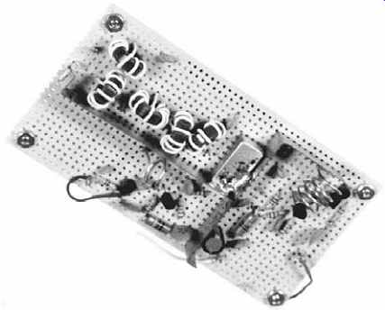
FIG. 6 The use of shielding on perfboard.
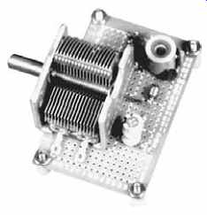
FIG. 7 VFO circuit build on perfboard.
Chassis and cabinets
It is probably wise to build RF projects inside shielded metal packages wherever possible. This approach to construction will prevent external interference from harming the operation of the circuit and prevent radiation from the circuit from interfering with external devices. FIG. 8 shows two views of an RF project built in side an aluminum chassis box; FIG. 8A shows the assembled box and FIG. 8B shows an internal view. These boxes have flanged edges on the top portion that over lap the metal side/bottom panel. This overlap is important for interference reduction. Shun those cheaper chassis boxes that use a butt fit, with only a couple of nipples and dimples to join the boxes together. Those boxes do not shield well.
The input and output terminals of the circuit in FIG. 8 are SO-239 "UHF" coaxial connectors. Such connectors are commonly used as the antenna terminal on shortwave radio receivers. Alternatives include "RCA phono jacks" and "BNC" coaxial connectors. Select the connector that is most appropriate to your application.
RF shielded boxes
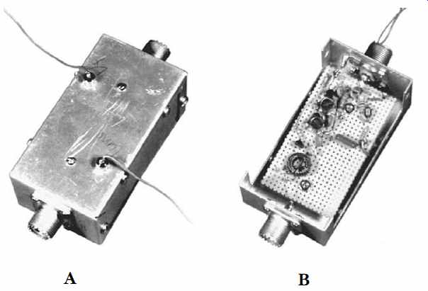
FIG. 8 Shielded RF construction: (A) closed box showing dc connections
made via coaxial capacitors; (B) box opened.
At one time, more than 2 decades ago, I loathed small RF electronic projects above about 40-m as "too hard." As I grew in confidence, I learned a few things about RF construction (e.g., layout, grounding, and shielding) and found that by following the rules, one can be as successful building RF stuff as at lower frequencies.
One problem that has always been something of a hassle, however, is the shielding that is required. You could learn layout and grounding, but shielding usually required a better box than I had. Most of the low-cost aluminum electronic hobbyist boxes on the market are alright for dc to the AM broadcast band, but as frequency climbs into the HF and VHF region, problems begin to surface. What you thought was shielded "t'ain't." If you've read my columns or feature articles over the years, you will recall that I caution RF constructors to use the kind of aluminum box with an overlapping flange of at least 0.25 , and a good tight fit. Many hobbyist-grade boxes on the market just simply are not good enough.
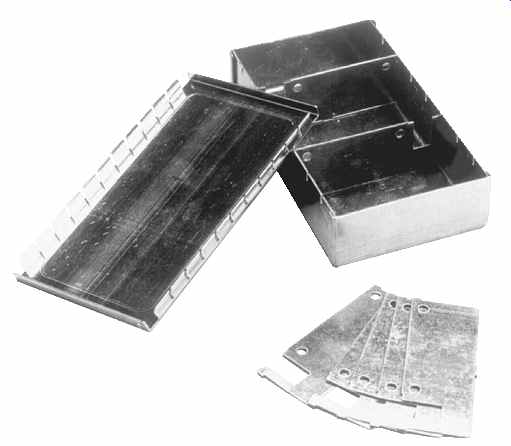
FIG. 9 RF project box with superior shielding because of the finger-grip design of the top cover (one of a series made by SESCOM).
SESCOM makes a line of cabinets, 19 racks, rack mount boxes, and RF shielded boxes. Their catalog has a lot of interesting items for radio and electronic hobbyist constructors. I was particularly taken by their line of RF shielded boxes. Why? Because it seems that RF projects are the main things I've built for the past 10 years.
FIG. 9 shows one of the SESCOM RF shielded steel boxes in their SB-x line.
Notice that it uses the "finger" construction in order to get a good RF-tight fit be tween the lid and the body of the box. Also notice that the box comes with some snap-in partitions for internal shielding between sections. The box body is punched to accept the tabs on these internal partitions, which can then be soldered in place for even better stability and shielding.
At first, I was a little concerned about the material; the boxes are made of hot tin-plated steel rather than aluminum. The tin plating makes soldering easy, but steel is hard on drill bits. I found, however, in experimenting with the SB-5 box supplied to me by SESCOM that a good-quality set of drill bits had no difficulty making a hole.
Sure, if you use old, dull drill bits and lean on the drill like Attila the Hun, then you'll surely burn it out. But by using a good-quality, sharp bit and good workmanship practices to make the hole, there is no real problem.
The boxes come in 11 sizes from 2.1 x 1.9 footprint to a 6.4 x 2.7 footprint, with heights of 0.63, 1.0, or 1.1. Prices compare quite favorably with the prices of the better-quality aluminum boxes that don't shield so well at RF frequencies.
The small project in FIG. 10 is a small RF preselector for the AM broadcast band. It boosts weak signals and reduces interference from nearby stations. The tuning capacitor is mounted to the front panel and is fitted with a knob to facilitate tuning. An on/off switch is also mounted on the front panel (a battery pack inside the aluminum chassis box provides dc power). The inductor that works with the capacitor is passed through the perfboard (where the rest of the circuit is located) to the rear panel (where its adjustment slug can be reached).
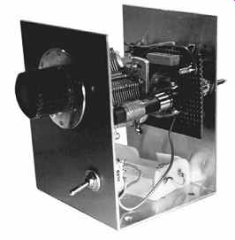
FIG. 10 Battery-powered RF project.
The project in FIG. 11 is a test that I built for checking out direct-conversion receiver designs. The circuit boards are designed to be modularized so that different sections of the circuit can easily be replaced with new designs. This approach allows comparison (on an "apples versus apples" basis) of different circuit designs.
Coaxial cable transmission line ("coax")
Perhaps the most common form of transmission line for shortwave and VHF/UHF receivers is coaxial cable. "Coax" consists of two conductors arranged concentric to each other and is called coaxial because the two conductors share the same center axis ( FIG. 12). The inner conductor will be a solid or stranded wire, and the other conductor forms a shield. For the coax types used on receivers, the shield will be a braided conductor, although some multistranded types are also sometimes seen. Coaxial cable intended for television antenna systems has a 75-ohm characteristic impedance and uses metal foil for the outer conductor. That type of outer conductor results in a low-loss cable over a wide frequency range but does not work too well for most applications outside of the TV world. The problem is that the foil is aluminum, which doesn't take solder. The coaxial connectors used for those antennas are generally Type-F crimp-on connectors and have too high of a casualty rate for other uses.
The inner insulator separating the two conductors is the dielectric, of which there are several types; polyethylene, polyfoam, and Teflon are common (although the latter is used primarily at high-UHF and microwave frequencies). The velocity factor (V) of the coax is a function of which dielectric is used and is outlined as follows:
Dielectric type -- Velocity factor
Polyethylene 0.66
Polyfoam 0.80
Teflon 0.70
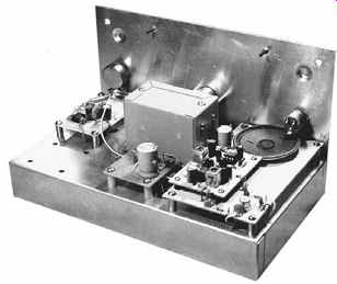
FIG. 11 Receiver chassis used as a "test bench" to try various
modifications to a basic design.
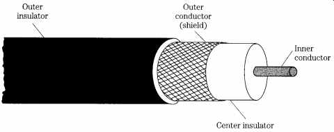
FIG. 12 Coaxial cable (cut-away view).
Coaxial cable is available in a number of characteristic impedances from about 35 to 125 ohm, but the vast majority of types are either 52- or 75-ohm impedances. Several types that are popular with receiver antenna constructors include the following:
RG-8/U or RG-8/AU 52 _ Large diameter RG-58/U or RG-58/AU 52 _ Small diameter RG-174/U or RG-174/AU 52 _ Tiny diameter RG-11/U or RG-11/AU 75 _ Large diameter RG-59/U or RG-59/AU 75 ohm Small diameter
Although the large-diameter types are somewhat lower-loss cables than the small diameters, the principal advantage of the larger cable is in power-handling capability. Although this is an important factor for ham radio operators, it is totally unimportant to receiver operators. Unless there is a long run (well over 100 feet), where cumulative losses become important, then it is usually more practical on receiver antennas to opt for the small-diameter (RG-58/U and RG-59/U) cables; they are a lot easier to handle. The tiny-diameter RG-174 is sometimes used on receiver antennas, but its principal use seems to be connection between devices (e.g., receiver and either preselector or ATU), in balun and coaxial phase shifters, and in instrumentation applications.
Installing coaxial connectors
One of the mysteries faced by newcomers to the radio hobbies is the small matter of installing coaxial connectors. These connectors are used to electrically and mechanically fasten the coaxial cable transmission line from the antenna to the receiver. There are two basic forms of coaxial connector, both of which are shown in FIG. 13 (along with an alligator clip and a banana-tip plug for size comparison). The larger connector is the PL-259 UHF connector, which is probably the most-common form used on radio receivers and transmitters (do not take the "UHF" too seriously, it is used at all frequencies). The PL-259 is a male connector, and it mates with the SO-239 female coaxial connector.
The smaller connector in FIG. 12 is a BNC connector. It is used mostly on electronic instrumentation, although it is used in some receivers (especially in handheld radios).
The BNC connector is a bit difficult, and very tedious, to correctly install so I recommend that most readers do as I do: Buy them already mounted on the wire.
But the PL-259 connector is another matter. Besides not being readily available al ready mounted very often, it is relatively easy to install.
FIG. 14A shows the PL-259 coaxial connector disassembled. Also shown in FIG. 14A is the diameter-reducing adapter that makes the connector suitable for use with smaller cables. Without the adapter, the PL-259 connector is used for RG 8/U and RG-11/U coaxial cable, but with the correct adapter, it will be used with smaller RG-58/U or RG-59/U cables (different adapters are needed for each type).
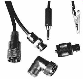
FIG. 13 Various types of coaxial connectors, cable ends, and adapters.
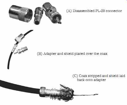
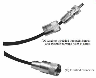
FIG. 14 Installing the PL-259 UHF connector.
(A) Disassembled PL-29 connector (B) Adapter and shield placed over the coax (C) Coax stripped and shield laid back onto adapter (D) Adapter threaded into main barrel and soldered through holes in barrel (E) Finished connector.
-----------
The first step is to slip the adapter and thread the outer shell of the PL-259 over the end of the cable ( FIG. 14B). You will be surprised at how many times, after the connector is installed, you find that one of these components is still sitting on the workbench -- requiring the whole job to be redone (sigh). If the cable is short enough that these components are likely to fall off the other end, or if the cable is dangling a particularly long distance, then it might be wise to trap the adapter and outer shell in a knotted loop of wire (note: the knot should not be so tight as to kink the cable).
The second step is to prepare the coaxial cable. There are a number of tools for stripping coaxial cable, but they are expensive and not terribly cost-effective for anyone who does not do this stuff for a living. You can do just as effective a job with a scalpel or X-acto knife, either of which can be bought at hobby stores and some electronics parts stores. Follow these steps in preparing the cable:
1. Make a circumscribed cut around the body of the cable ¾ from the end, and then make a longitudinal cut from the first cut to the end.
2. Now strip the outer insulation from the coax, exposing the shielded outer conductor.
3. Using a small, pointed tool, carefully unbraid the shield, being sure to separate the strands making up the shield. Lay it back over the outer insulation, out of the way.
4. Finally, using a wire stripper, side cutters or the scalpel, strip 5/8 of the inner insulation away, exposing the inner conductor. You should now have 5/8 of inner conductor and 3/8 of inner insulation exposed, and the outer shield de-stranded and laid back over the outer insulation.
Next, slide the adapter up to the edge of the outer insulator and lay the unbraided outer conductor over the adapter ( FIG. 14C). Be sure that the shield strands are neatly arranged and then, using side cutters, neatly trim it to avoid interfering with the threads. Once the shield is laid onto the adapter, slip the connector over the adapter and tighten the threads ( FIG. 14D). Some of the threads should be visible in the solder holes that are found in the groove ahead of the threads. It might be a good idea to use an ohmmeter or continuity connector to be sure that there is no electrical connection between the shield and inner conductor (indicating a short circuit).
Warning Soldering involves using a hot soldering iron. The connector will become dangerously hot to the touch. Handle the connector with a tool or cloth covering.
• Solder the inner conductor to the center pin of the PL-259. Use a 100-W or greater soldering gun, not a low-heat soldering pencil.
• Solder the shield to the connector through the holes in the groove.
• Thread the outer shell of the connector over the body of the connector.
After you make a final test to make sure there is no short circuit, the connector is ready for use ( FIG. 14E).