AMAZON multi-meters discounts AMAZON oscilloscope discounts
The purpose of the detector or demodulator circuits is to recover the intelligence impressed on the radio carrier wave at the transmitter. This process is called demodulation and the circuits used to accomplish this are called demodulators.
They are also called second detectors in superheterodyne receivers.
In a superheterodyne receiver the detector or demodulator circuit is placed between the IF amplifier and the audio amplifier (Fig. 27-1). This position is the same in AM, FM, pulse modulation, and digital receivers (although in digital receivers the demodulator might be in a circuit called a MODEM).
AM envelope detectors
An amplitude modulation (AM) signal consists of a slow audio signal which revolves around an average radio frequency (RF) carrier signal. It is essentially a multiplication or mixing process in which the RF carrier and AF signals are both output, along with the (RF _ AF) and (RF _ AF) signals. Because of the selectivity of the transmitter circuits, only the RF carrier and the sum and difference signals appear in the output. The AF signal is suppressed. The sum signal (RF _ AF) is known as the upper sideband (USB) while the difference signal (RF _ AF) is known as the lower sideband (LSB). Because of this action, the bandwidth of the AM signal is deter mined by the highest audio frequency transmitted and is equal to twice that frequency. A total of 66.67% of the RF power in an AM signal is in the carrier so only 33.33% is split between two sidebands.
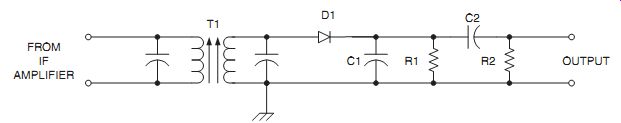
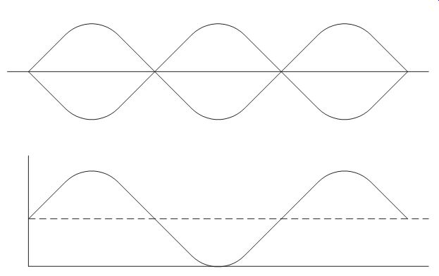
Figure 27-2 shows a simple AM envelope detector circuit while Fig. 27-3 shows the waveforms associated with this circuit. The circuit consists of a signal diode rectifier connected to the output of an IF amplifier. There is a capacitor (C1) and resistive load connected to the rectifier. When the input signal is received (Fig. 27-3A) it is rectified (Fig. 27-3B), producing an average current output that translates to the voltage waveform of Fig. 27-3C.
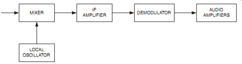
27-1 Location of the demodulator circuit.
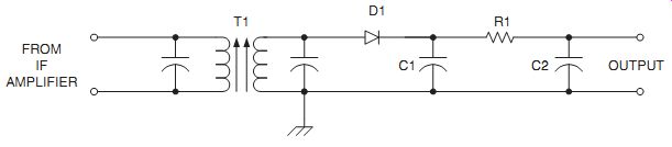
27-2 Simple envelope detector.
The capacitor is charged to a value equal to 0.637 times the peak voltage (which is the average value) and then scales upward with modulation to the full peak value.
Low-pass filter R1C2 takes out the residual RF/IF signal.
The important attribute of a demodulator is for it to have a nonlinear response, preferably with a sharp cutoff. Vacuum tubes, bipolar transistors, and field-effect transistors possess these characteristics, but so does the simple diode rectifier.
Figure 27-4 shows the input and output characteristics compared with the diode's I-vs-V curve. At low signal levels the diode acts like a square law detector, but at higher signal levels the operation is somewhat linear.
Consider a diode with an I-vs-V characteristic of:
(27-1)
(27-2)
(27-3)
(27-4)
27-3 AM detector outputs.
where:
m is the modulation index
fc is the carrier frequency
A is the peak amplitude
a0, a1, and a2 are constants.
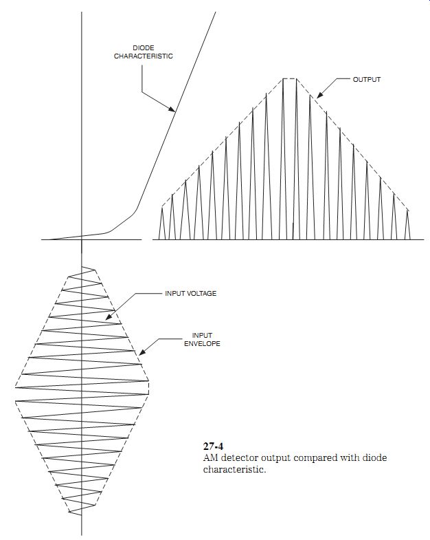
27-4 AM detector output compared with diode characteristic.
27-5 Unfiltered AM output.
The terms in the brackets are the modulation and distortion products. The second-order terms are modulation and distortion, where the higher-order terms are distortion only. What falls out of the equation is that to keep distortion low, modulation index (m) must be low as well.
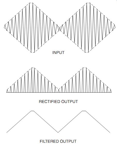
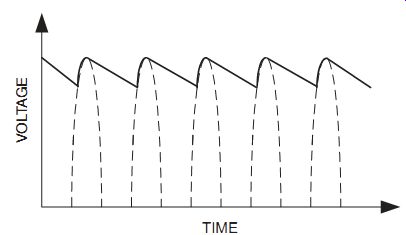
Figure 27-5 shows what happens at the capacitor. The dotted lines represent the output of the diode, which is a half-wave rectified RF/IF signal; the heavy line represents the capacitor voltage (Vc). The capacitor charges to the peak value and then the diode cuts off. The voltage across the capacitor drops slightly to the point where its voltage is equal to the input voltage, when it turns on again. The diode may be modeled as a switch with resistance. During the non-conduction period, the switch is open and the capacitor discharges. During the conduction period, the "switch" con ducts and charges the capacitor. The waveform across the capacitor when there is no modulation is close to a sawtooth at the carrier frequency (fc) and it represents the residual RF. These are eliminated in the RC filter to follow the envelope detector (R1C2) and the response of the amplifiers to follow the detector. These components are typically about 30 dB below the carrier level.
The maximum time constant of the filtering action of C1, plus (R1 _ R), where R is the resistance to ground (typically a volume control), that can be accommodated depends on the maximum audio frequency that must be processed. A frequency of 3000 Hz and a time constant of 10 _S yields:

(27-5)
.....which produces an output reduction of.....

(27-6)
... which is 0.16 dB. At 10 KHz these values are 0.628 and 1.18, or 1.44 dB.
Figure 27-6 shows a version of the envelope detector that uses a high-pass filter at the output. The time constant referred to above is the time constant R1C1 and eliminates the residual RF/IF signal. The time constant R2C2 is set to eliminate low-frequency hum and noise. The speech requirement in communications receivers is 300 to 3000 Hz so a 60-Hz hum is easily accommodated. For broadcast receivers, the low-frequency audio is on the order of 100 Hz so this method is less workable.
27-6 Simple envelope detector.
In the linear mode of operation of the diode, the modulation index for which distortion begins is:
The distortion will be small if
(27-8)
where .......
Zm is the impedance of the circuit at the modulating frequency
Equation (27-7) reduces to this form when Rd << R1 and Zm _ R2.
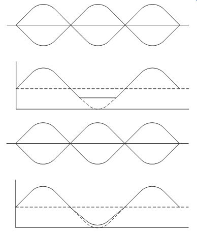
Figure 27-7 shows three situations of input waveform and output waveform.
Figure 27-7A is the situation in which there is no distortion of the output waveform.
Although this waveform never occurs in real circuits, it is included for the sake of making the comparison. In Fig. 27-7B, the circuit clips the negative peaks of the modulating signal. In Fig. 27-7C we see an example of diagonal clipping. This form of clipping occurs when Zm is not resistive.
27-7 (A) Proper AM detection; (B) Clipping evident; (C) odd form of clipping
present.
27-7 Continued.
Another form of distortion occurs when the RF/IF waveform is distorted. Both in-phase and quadrature distortion can occur in the RF/IF waveform, especially if the bandpass filters used in the RF/IF circuit have complex poles and zeros distributed asymmetrically about the filter center frequency or when the carrier is not tuned to the exact center of the filter passband.
Noise
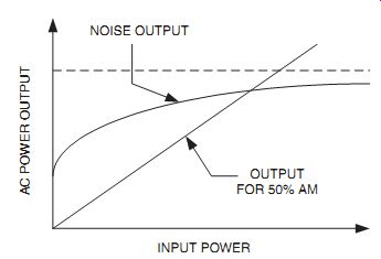
All radio reception is basically a game of signal-to-noise ratio (SNR). If the SNR is not advantageous, then the receiver ultimately fails. At low signal levels (Fig. 27-8) the SNR is poor and the noise dominates the output. As the signal level increases, however, the noise level increases but at a slower rate than the signal output. The noise level comes to rest (see dotted line in Fig. 27-8) about 3.7 dB over the no-carrier state but the signal level continues upward.
27-8 Noise vs. output for 50% AM modulation.
Balanced demodulators
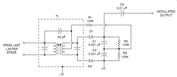
Figure 27-9 shows two examples of balanced or full-wave demodulator circuits. These circuits work generally better than the half-wave version shown earlier. Figure 27-9A shows the circuit for a conventional full-wave circuit. It depends on two diodes and a center-tapped transformer (T1). It works like the power-supply circuit of the same type. The center tap on the transformer establishes the zero point, or common, so the polarities of the voltages at the ends of the secondary of T1 are equal but opposite. When the top of the secondary is positive with respect to the bottom, diode D1 conducts and charges capacitor C1. On the opposite half-cycle, the opposite occurs. In that instance, the secondary is reverse polarity, so the bottom is more positive than the top. This turns off D1 and turns on D2, causing it to conduct and charge C1.
Figure 27-9B shows a bridge rectified version of the AM envelope detector.
When the top of the T1 secondary is positive with respect to the bottom, diodes D2 and D3 conduct, charging C1. When the bottom of the T1 secondary is positive with respect to the top, diodes D1 and D4 conduct, charging the capacitor. Hence, since these conditions occur on alternate half-cycles of the input waveform, full-wave rectification occurs.
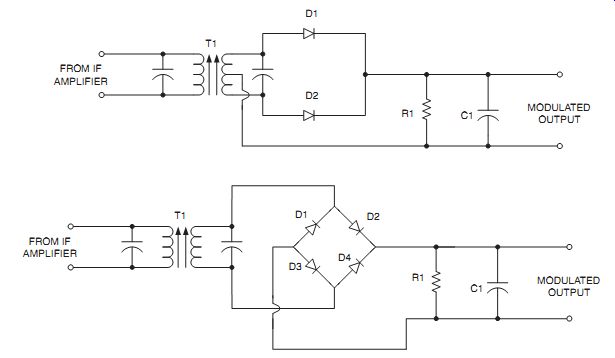
27-9 (A) Full wave AM envelope detector; (B) full wave bridge type AM envelope
detector.
Synchronous AM demodulation
One of the factors that controls the comfort level of listening to demodulated AM transmissions is that the carrier and two sidebands fade out of phase with each other. This can be overcome with quasi-synchronous demodulation or synchronous demodulation. Both require that the incoming carrier be eliminated. The difference is that in quasisynchronous demodulation the reinserted carrier is not in phase with the original, whereas in synchronous demodulation it is.
Quasisynchronous demodulation is much like the demodulators discussed below under single-sideband demodulators. They have a beat frequency oscillator to re place the carrier with an out-of-phase version. As long as the signal does not drop to zero, the process works fine. But when the signal drops to zero, as it does under deep fading, then the process falls down and synchronous demodulation wins. In synchronous demodulation the reinserted carrier is in phase with the original carrier signal. The circuit must phase lock to the original carrier.
Double-sideband (DSBSC) and single-sideband (SSBSC) suppressed carrier demodulators
Double- and single-sideband suppressed carriers are a lot more efficient than straight AM. In straight AM, the carrier contains two-thirds of the RF power, with one-third split between the two sidebands. Interestingly enough, the entire intelligent content of the speech waveform is fully contained within one sideband, so the other sideband (and carrier) are superfluous.
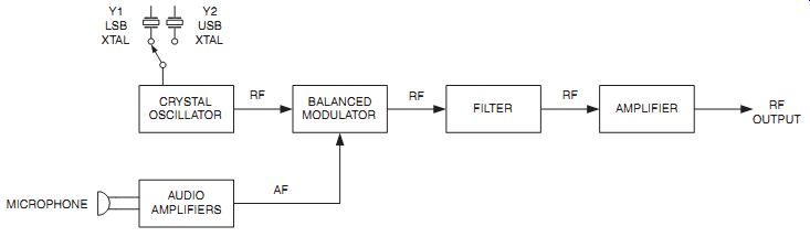
Figure 27-10 shows a single-sideband suppressed carrier (SSBSC, usually shortened to "SSB") transmitter. The heart of the circuit is a balanced modulator circuit.
This circuit is balanced to produce an RF output from the crystal oscillator only when the audio frequency (AF) signal is present. As a result, the carrier is sup pressed in the double-sideband output.
27-10 Location of SSB crystal frequencies.
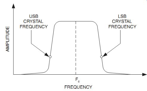
The next stage is a symmetrical bandpass filter circuit that removes the un wanted sideband, leaving only the desired sideband. The crystal oscillator deter mines which sideband is generated. By positioning the frequency of the oscillator on the lower skirt of the filter, an upper sideband (USB) signal is generated. By positioning the frequency of the oscillator on the upper skirt of the filter, the lower side band (LSB) is generated. This is shown in Fig. 27-11. In this figure, Fc is the center frequency of the filter while the LSB and USB frequencies are shown.
Following the filter circuit is any amplification or frequency mixing needed to accomplish the purposes of the transmitter. Contrary to AM transmitters, all stages following the balanced modulator are expected to be linear amplifiers. This is be cause nonlinear stages will distort the envelope of the SSB signal. This means that heterodyning must be used rather than multipliers or other nonlinear means in order to translate the frequencies. It is generally the way of SSB transmitter designers to generate the SSB signal at a fixed pair of frequencies and then heterodyne them to the desired operating frequency. There is also a phasing method of generating an SSB signal. Double-sideband transmitters are the same as Fig. 27-10, except that the filter is not present.
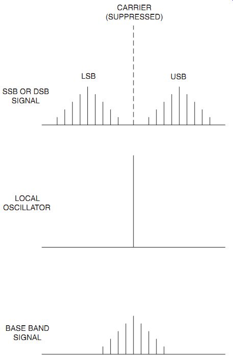
27-11 SSB or DSB signal.
The basis for SSB and DSB demodulation is the product detector circuit.
Figure 27-12 shows basis for product detection. In Fig. 27-12A we see the SSB or DSB signal, with the carrier suppressed (it's actually a DSB signal, but an SSB signal would lack the other sideband). This signal is combined with a strong local oscillator signal (called a beat frequency oscillator or BFO; Fig. 27-12B) to produce the base band signal (Fig. 27-12C).
27-12 Simple product detector.
27-13 Four-diode product detector.
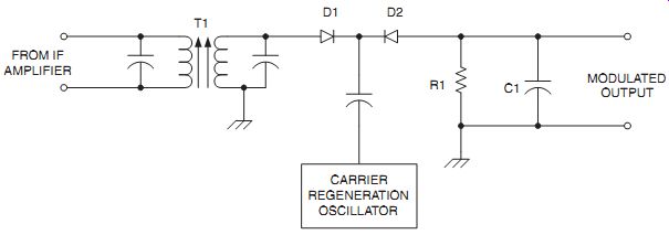
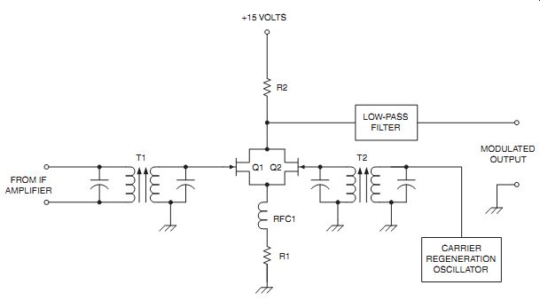
Figure 27-13 shows a simple form of product detector circuit. It is like the envelope detector except for the extra diode (D2) and a carrier regeneration oscillator (also called a BFO). The circuit works by switching the diodes into and out of conduction with the oscillator signal. When the output of the oscillator is negative, the diodes will conduct, passing signal to the output. But on positive excursions of the local oscillator signal the diodes are blocked from conducting by the bias produced by the oscillator signal. The residual RF/IF signal is filtered out by capacitor C1.
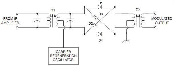
A superior circuit is shown in Fig. 27-14. This circuit is a balanced product detector. It consists of a balanced ring demodulator coupled through a pair of center tapped transformers (T1 and T2). Transformer T1 is the last IF transformer. It has a center-tapped secondary to receive the strong local oscillator signal used for carrier regeneration. The output transformer (T2) is also center-tapped but in that case the center-tap is grounded.
27-14 Transistor product detector.
The circuit works by switching in and out of the circuit pairs of diodes on alternate half-cycles of the SSB waveform. Consider first circuit action when no signal is present. That leaves only the local oscillator signal, which is applied to the common point on the transformer T1 secondary. That means that the ends of the transformer will be positive and negative at the same time. Under this circumstance, the diodes D1-D4 conduct and then diodes D2-D3 conduct, but both signals are nulled in the primary winding of T2. This occurs because both signals are the same.
When the top of the T1 secondary is positive with respect to the bottom, and the local oscillator signal is positive, then diodes D1 and D2 conduct, creating an unbalanced situation, which results in an output. Similarly, when the situation is reversed only the D2-D3 diodes conduct and the others are cut off. Thus, the local oscillator controls the output of the product detector.
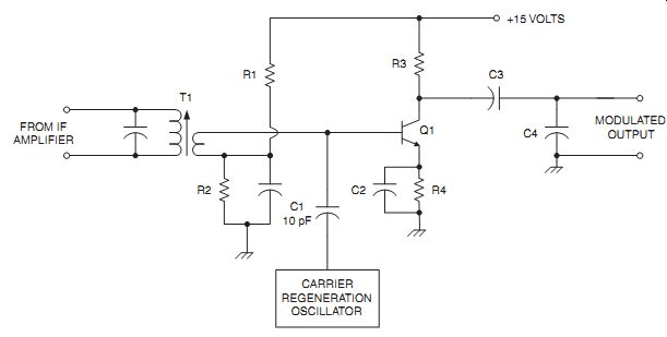
Figure 27-15 shows a circuit in which a bipolar transistor is used as a product detector. The circuit would act like any amplifier, except that the base of the transistor is controlled by the local oscillator. The SSB signal is applied through the low impedance secondary of T1 and would ordinarily be amplified by Q1. But the quenching action of the local oscillator prohibits this action. The transistor is alternately cut off and cut on by the local oscillator circuit and that creates the nonlinearity needed to demodulate the waveform.
27-15 Dual JFET product detector.
A differential pair of junction field effect transistors (JFETs) is used in Fig. 27-16 to produce the product detection. The SSB signal is applied to the gate of Q1, while the local oscillator signal is used to disrupt the operation of the circuit from the Q2 side. Keep in mind that the local oscillator signal is very much greater in amplitude than the SSB signal. A low-pass filter tuned to the spectrum that is to be recovered (typically audio) is connected to the common drain circuits and thence to the output.
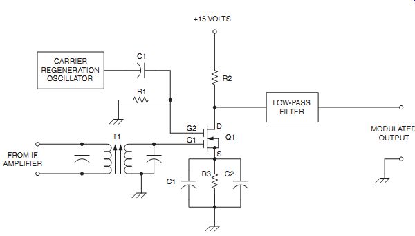
27-16 MOSFET product detector.
A dual-gate MOSFET transistor is the subject of Fig. 27-17. The normal signal input of the MOSFET, gate 1, is used to receive the SSB signal from the IF amplifier.
The MOSFET is turned on and off by the local oscillator signal applied to gate 2.
Again, an audio low-pass filter is present at the output (drain) circuit to limit the residual IF signal that gets through to the modulated output.
27-17 MC-1496 product detector.
Notice in this circuit that there are two capacitors in the source circuit of the MOSFET transistor (C1 and C2). Typically, one of these will be for RF and the other for AF, although with modern capacitors it might not be strictly necessary.
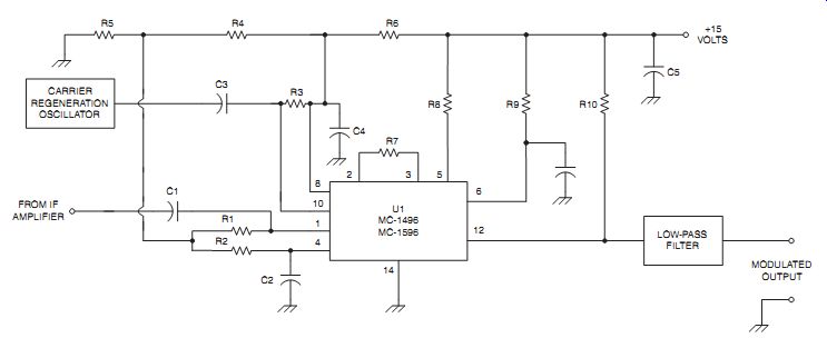
An integrated circuit SSB product detector is shown in Fig. 27-18. This circuit is based on the MC-1496 analog multiplier chip. It contains a transconductance cell de modulator that is switched on and off by the action of the local oscillator. The SSB IF signal is input through pin no. 1 and the local oscillator through pin no. 10. The alternate pins in each case are biased and not otherwise used.
27-18 Filter-type SSB transmitter.
27-19 Phasing type SSB transmitter.
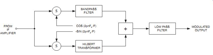
Phasing method
The methods for demodulating an SSB or DSB signal thus far presented have been product detectors. There is also a phasing method used in some cases. Figure 27-19 shows this method in block diagram form. This method splits the SSB IF signal into two paths, I and Q. They are mixed with a pair of signals that are the same except for phasing. The I signal is mixed with the cos (2_nFc/F) version of the local oscillator signal while the Q is mixed with the _sin (2_nFc/F) version of the same signal. The Q channel is passed through a Hilbert transformer, which has the effect of further phase shifting it by 90 degree . The I channel signal is delayed an amount equal to the delay of the Q channel signal or (N _ 1)/2 samples. The two signals are then summed in a linear mixer circuit to produce the output. This method will yield the lower sideband part of the signal. If we subtract the two signals instead of adding them we will yield the upper sideband signal.
FM and PM demodulator circuits
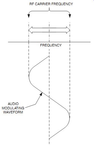
Frequency modulation and phase modulation are examples of angle modulation. Figure 27-20 shows this action graphically. The audio signal causes the frequency (or phase) to shift plus and minus from the quiescent value, which exists when there is no modulation present. Frequency and phase modulation are different but similar enough to make the demodulation schemes the same. The difference be tween FM and PM is that the phase modulation needs no preemphasis curve to the audio waveform (it does it naturally) while the frequency modulation transmitter is preemphasized for noise abatement.
27-20 FM modulation.
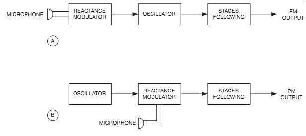
Another difference between FM and PM transmitters is the location of the reactance modulator used to generate the modulated signal. In the FM transmitter the reactance modulator is part of the frequency determining circuitry, whereas in the PM transmitter it follows that circuitry.
Discriminator circuits
One of the classic FM discriminator circuits is shown in Fig. 27-21. This circuit uses a special transformer that has two secondary windings. One secondary winding is tuned slightly above the IF frequency while the other is tuned the same amount below the IF frequency. The two frequencies are spaced slightly more than the expected transmitter swing. Their outputs are combined in a differential pair of diodes (D1 and D2). The outputs of the diodes are connected to load resistors R1 and R2.
Normally, when the signal is unmodulated, the algebraic sum of the two diodes out puts is zero, resulting in zero output. When the frequency or phase swings above the quiescent value, one diode will conduct higher than the other, resulting in an imbalance across R1 and R2. That produces an output. Similarly, when the frequency or phase drops below the quiescent value, then the opposite situation exists. The other diode will conduct harder and produce an output of the opposite polarity.
27-21 Two forms of angular modulation (A) FM, (B) PM.
27-22 Dual-tuned discriminator.
27-23 Single tuned discriminator.
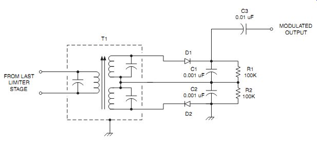
Foster-Seeley discriminator circuits
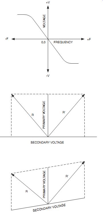
The Foster-Seeley discriminator circuit is shown in Fig. 27-22, while the wave forms are shown in Fig. 27-23. This circuit requires only two tuned circuits rather than the three required by the previous circuit. The output voltage is the algebraic sum of the voltages developed across the R2 and R3 load resistances. Figure 27-23A shows the relationship of the output voltage and the frequency.
The primary tuned circuit is in series with both halves of the secondary winding.
When the signal is unmodulated, the IF voltage across the secondary is 90 degree out of phase with the primary voltage. This makes the voltages applied to each diode equal but out of phase (Fig. 27-23B), resulting in zero output. But consider what happens when the frequency deviates (Fig. 27-23C). The voltages applied to the diodes are no longer equal but opposite, and that creates an output from the detector that is frequency- or phase-sensitive. As the input frequency deviates back and forth across the frequency of the tuned circuit an audio signal is created equal to the modulated frequency.
In order for the FM/PM transmitter to be received "noise-free" it is necessary to precede the discriminator circuit with a limiter circuit. This circuit limits the positive and negative voltage excursions of the IF signal, thus clipping off AM noise.
Ratio detector circuits
27-24 Waveforms for FM demodulation.
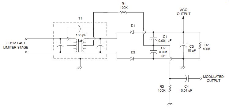
The ratio detector circuit is shown in Fig. 27-24. This circuit uses a special transformer in which there is a small capacitor between the center tap on the primary winding and the center tap on the secondary winding. Note that the diodes are connected to aid each other rather than buck each other, as was the case in the Foster-Seeley discriminator circuit. When the signal is unmodulated, the voltage appearing across R3 is one-half the AGC (automatic gain control) voltage appearing across R2 because the contribution of each diode is the same. However, that situation changes as the input signal is modulated above or below the center frequency. In that case, the relative contribution of each diode changes. The total output voltage is equal to their ratio; hence the name ratio detector.
There are several advantages of a ratio detector over a Foster-Seeley discriminator. First, there is no need for a limiter amplifier ahead of the ratio detector, as there is with the Foster-Seeley discriminator. Furthermore, the circuit provides an AGC voltage, which can be used to control the gain of preceding RF or IF amplifier stages. However, the ratio detector is sensitive to AM variations of the incoming signal, so the AGC should be used on the stage preceding the ratio detector to limit those AM excursions. The capacitor, C3, also helps eliminate the AM component of the signal, which is noise.
27-25 Ratio detector.
27-26 Coil-less FM detector.
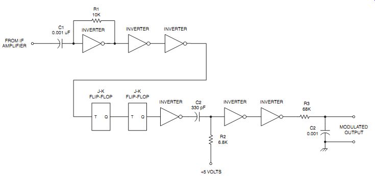
Pulse-counting detectors
The FM/PM detectors thus far considered have required special transformers to make the work. In this section we are going to look at a species of coil-less FM detector. The pulse-counting detector is shown in Fig. 27-25. This circuit uses two integrated circuits, a hex inverter and a dual J-K flip-flop. The hex inverter has six inverter stages. The first stage is used as an amplifier, while the next two are used to produce an output that is free of AM noise (most noise is AM). This is followed by a pair of divide-by-two (total divide-by-four) stages consisting of a pair of J-K flip flops. An inverter at the output of the flip-flops is used to drive the input of a half monostable multivibrator that has a period equal to about one-half the period of the unmodulated input signal. The output of the half-monostable is a time-varying pulse train that varies with the audio modulation applied to the input signal. It is realized as audio in the low-pass filter consisting of R3-C2.
Another circuit, shown in block form, used a zero-crossing detector and a limiter amplifier to eliminate the AM excursions that are noise to an FM/PM signal. The out put of the zero-crossing detector triggers a monostable multivibrator circuit. The output of the monostable is a pulse train that varies according to the modulating frequency applied. This is realized in a low-pass filter circuit.

27-27 Block diagram of coil-less FM detector.
Phase locked loop FM/PM detectors
The phase locked loop (PLL) circuit can be used as an FM demodulator if its control voltage is monitored. Figure 27-27A shows the basic PLL circuit. It consists of a voltage-controlled oscillator (VCO), phase detector, low-pass filter, and an amplifier. The FM signal from the IF amplifier is applied to one port of the phase detector, and the output of the VCO is connected to the other port. When the two frequencies are equal, there is no output from the circuit (or, the value is quiescent).
When the FM IF signal deviates above or below the frequency of the VCO, there will be an error term generated. This error signal is processed in the low-pass filter and amplifier to control the VCO. Its purpose is to drive the VCO back on the right frequency. It's this error signal that becomes the modulated output of the PLL FM de modulator circuit. Figure 27-27B shows a PLL based on the NE-565 PLL integrated circuit. The resonant frequency is set by R1 and C1, which should be the center frequency of the FM signal. As the signal deviates up and down, the error voltage is monitored and becomes the modulated output signal.
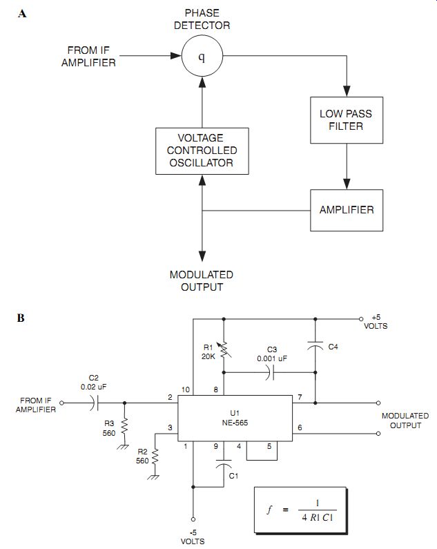
27-28 (A) Phase locked loop circuit; (B) NE-565 FM detector.
Quadrature detector
Figure 27-28 shows the quadrature detector circuit. This circuit is implemented in integrated circuit form (e.g., MC-1357P and CA-3089) and uses a single phase-shifting external coil to accomplish its goals. This is probably the most widely used form of FM demodulator in use today.
The typical quadrature detector IC uses a series of wideband amplifiers to boost the signal and limit it, eliminating the AM noise modulation that often rides on the signal. This signal is applied to the signal splitter. The two outputs of the signal splitter are applied to a gated synchronous detector, but one is phase-shifted 90 degree . The output of the gated synchronous detector is the modulated audio.