AMAZON multi-meters discounts AMAZON oscilloscope discounts
Take a simple, everyday thing like a coffee and soup vending-machine.
Before it delivers a cup of coffee, two things must happen: (i) some money must have been put in; and (ii) the button for 'coffee' must have been pressed. We can write down the requirement as money AND coffee button = coffee and represent this diagrammatically --see Fig. 1.
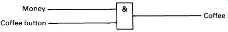
FIG. 1 an AND logic system.
Both inputs (money and coffee button) must be present before there is an output. If we want to design a system that gives soup as an alternative, then we need a schematic like the one shown in Fig. 2.
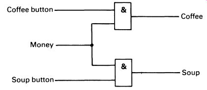
FIG. 2 a logic system using two AND gates
Notice that one of the inputs (money) is common to both gates. This, plus the other input, gives the relevant output. As far as it goes, the system is workable, but it has a design fault. Sooner or later someone will discover that if you press both buttons, you get coffee and soup. We could have predicted this by writing down a table of all possible combinations of logic inputs and their resulting outputs. Such a table is called a truth table, and a truth table for Fig. 2 is given in Fig. 3.
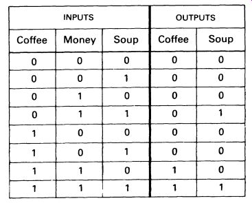
FIG. 3 a truth table for a coffee/soup vending machine
The last line is the one that shows up the problem. We can overcome our design problem by adding another stage to the logic, represented in diagram form by Fig. 4.
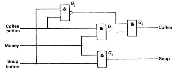
FIG. 4 a logic system for the coffee/soup vending machine.
We should examine the workings of this in more detail. G1 and G2 are our original system; G3 and G4 have been added. The symbol used for G3 is slightly different, the 0 on the output representing a negation. All this means is that the sense of the output is reversed-the output is always 'on' unless both inputs are also 'on' (in which case it is 'off). Thus the upper input of G4 is usually 'on', and when the lower input is also 'on' (coffee button AND money) the 'coffee' output is also on. If both buttons are pressed, the output of G3 goes off, suppressing the 'coffee' output.
All you get is soup, and it serves you right for trying to cheat! A truth table for Fig. 4 is given in Fig. 5.
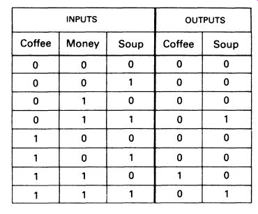
FIG. 5 a truth table for the system shown in Fig. 4
You have probably recognized the diagrams as logic diagrams, and the systems shown can be implemented, exactly as they are, using digital integrated circuits.
1. AND/NAND GATES
Before going any further with the system, it is worth pausing to look at the logic gates that are commonly used in simple logic systems. Fig. 6a shows AND and NAND gates. We met these in the coffee-machine logic, and their function should be obvious by now-but the truth table in Fig. 6b formalizes the functions. The output of the AND gate is 1 only when both inputs are also logic 1; the output of the NAND gate is 0 only when both inputs are logic 1.
2. OR/NOR GATES
Fig. 7 shows the symbols and truth tables for OR and NOR gates.
The output of the OR gate is 1 if either of the inputs is 1, or if both of them are 1. In the same way, the output of the NOR gate is 0 if either or both of the inputs are 1.
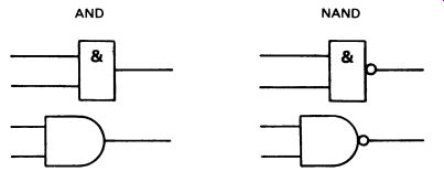
FIG. 6 (a) logic symbols for AND and NAND gates; the upper symbols
are the recommended lEG/British Standard symbols, while those below are
the American standard; both types of symbol are used, the American version
being the more common (b) truth tables for the AND and NAND gates
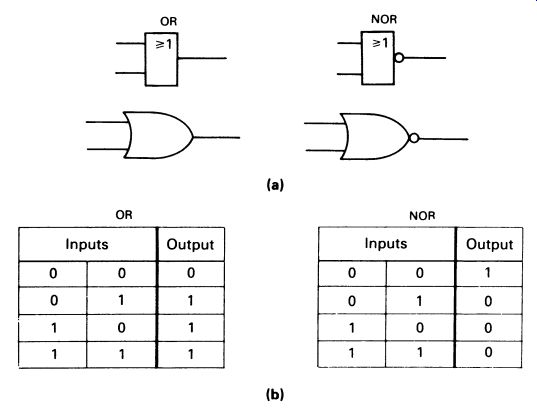
FIG. 7 OR and NOR gates, along with their truth tables; once again,
the upper symbols are IEC/BS, the lower ones the US standard
3. NOT GATE, OR INVERTER
Fig. 8 shows the simplest logic element (no truth table necessary!), the NOT gate, more usually called an inverter. It simply changes the sense of the input, 0 output for 1 input and vice versa.
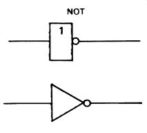
FIG. 8 a NOT gate (or inverter); IEC!BS symbol on top, US symbol
below
4. EX-OR GATES
Fig. 9 shows an Exclusive-OR gate, along with its truth table. The Exclusive-{)R gate is just like an ordinary OR gate, except that the output is only 1 when just one of the inputs is 1. If more than one input is at logic 1, or if all inputs are at logic 0, the output is 0. EX-OR gates are less commonly found than the AND/ NAND, OR/NOR varieties.
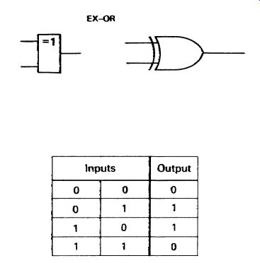
FIG. 9 an exclusive-OR gate, with its truth table; IEC!BS symbol
on the left.
5. MORE COMPLEX GATES
It is possible to ring the changes on the basic gates. Gates of all types often have more than two inputs--Fig. I 0 shows a CD4068 eight-input NAND gate. If one or more inputs are at logic 1, the output is 0. If all the inputs are 0, the output is l.
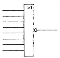
FIG. 10 an 8-input NOR gate, IEC/BS symbol. From now on, throughout
this guide, IECIBS symbols are used; the equivalent US symbol is easily
derived by comparison with Figures 19.6 to 19.9
Gate inputs can also be negated, reversing their sense. This could be done using an inverter in the input line (Fig. lla); or if the inverter is part of the same IC as the gate, it can be drawn like the one in Fig. llb.
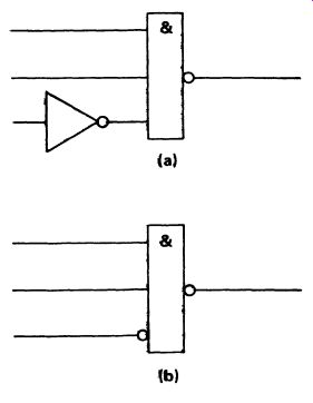
FIG. 11 a NAND gate with one input inverted-two alternative representations
6. MINIMIZATION OF GATES
It is only sensible to design any logic system with the smallest possible number of gates, all else (the price of different types of gate) being equal.
For simple systems it is usually possible to minimize the number of gates by inspection; for more complicated systems Boolean algebra can be used to formalize the problem and arrive at a solution (see N. M. Morris, Digital Electronic Circuits and Systems, Macmillan, 1974). Clearly, it takes only a short time to realize that the system in Fig. 12a can be reduced to the system in Fig. 12b without any change in its functioning. It is less obvious that Figures 19.13a and 19.13b are functionally the same-but it is obvious if you draw up the truth table for them.
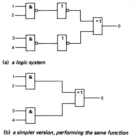
FIG. 12 (a) a logic system (b) a simpler version, performing the
same function
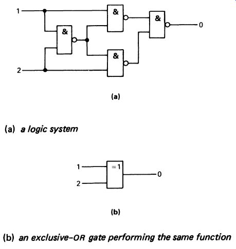
FIG. 13 (a) a logic system (b) an exclusive-OR gate performing the
same function
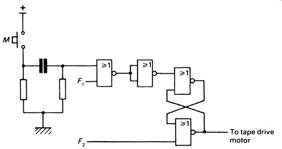
FIG. 14 a bistable control for a tape drive motor
Fig. 14 shows a simple logic system that was actually used in a cassette tape-recorder intended for use with a microcomputer. F 1 and F 2 are inputs controlled by the computer, to stop and start the recorder motor. The two gates on the right form a bistable (see Section 21) which 'latches' the motor on or off. Switch 'M' is for manual operation, and turns the motor on by applying a logic 1 pulse to the gate.
At first sight the circuit can be simplified by avoiding the double negation in the NOR gate and inverter, replacing them both with a single OR gate, as in Fig. 15. So why would a sensible (and cost-conscious) manufacturer prefer the more complicated version in Fig. 14? The answer lies in Fig. 16, which shows the pin-out of the SN74LS02 integrated circuit.
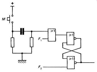
FIG. 15 a simpler but more expensive version of the circuit given
in Fig. 14
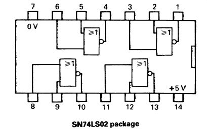
FIG. 16 the pin connections of the SN14LS02 quad NOR gate
This integrated circuit includes four NOR gates (it is known as 'quad 2-input NOR gate'), which is just right for the system in Fig. 14. You cannot obtain a single integrated circuit that incorporates an oR gate plus NOR gates, so the apparently simpler version in Fig. 15 actually requires two integrated circuits, which in turn means more circuit-board space, more soldered connections, and higher assembly costs. In almost all practical systems, minimization of components and cost is the requirement.
Reducing the number of gates in a given system may not always further that end.
Where large systems are involved (e.g. counters, clocks and computing circuits) it is almost always economic to use a large-scale integrated circuit (LSI) or even a microprocessor, despite the fact that only a fraction of the device's total capacity may be used. Very complicated LSI circuits are relatively cheap--a Z80 microprocessor chip cons less than twenty times as much as the simplest gate.
Having covered the basic types of gate, in the next section we shall consider the two major kinds of technology that are used in the implementation of integrated circuit logic elements.
QUESTIONS: SECTIONS 18 AND 19
1. Why is the binary system of numbers used in computers?
2. Sketch a logic system in which the following truth table is implemented:
3. Draw circuit symbols for (i) a 3-input NAND gate, (ii) an inverter, (iii) a 4-input OR gate with one negated input.
4. What is the largest (denary) number that can be represented by eight binary digits?
5. Draw a logic circuit including one EX-OR gate and one NAND ~te, any connections. Now construct a truth table for the circuit.