AMAZON multi-meters discounts AMAZON oscilloscope discounts
Although there are many ways of making integrated circuits, and several technologies are available to the manufacturer, only two major 'families' of general-purpose logic ICs have developed. The first, and oldest, family is TTL. TTL stands for 'transistor-transistor logic', this logic family having replaced the older (now obsolete) DTL-diode-transistor logic. The second logic family is CMOS (pronounced 'sea-moss') which stands for 'complementary metal oxide semiconductor'. Both families include a very large number of different devices: gates, flip-flops, counters, registers and many other 'building-block' elements. In many cases there are direct substitutes, but, as we shall see, it is not usually possible to mix devices from the two families.
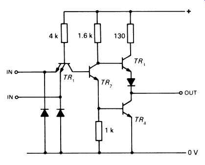
FIG. 1 a typical bipolar 2-input NAND gate
Both groups have their own special advantages and disadvantages, and when a designer is working on a digital system the choice of logic family will probably be one of his first decisions.
1. TTL
This family is based on the bipolar junction transistor, and was perhaps the first commonly available series of logic elements. Although the logic designer rarely needs to know how the inside of an IC works, it is instructive, when comparing logic families, to look at the workings of a simple gate. We can take as an example a 2-input NAND gate, numbered, appropriately enough, SN7400 in the TTL series. Fig. 1 shows the circuit of this gate.
Notice that the circuit has a familiar 'transistor amplifier' look about it, except that the circles round the transistors have been left out-they represent the encapsulations. The input transistor is also unusual, by discrete component standards, in that it has two emitters. The circuit operates as follows. TR2 is normally off (both inputs logic 0}, which means that TR3 is on, the 1.6 k-Ohm resistor providing the base current. TR4 is off, its base being clamped to 0 V by the 1 k-Ohm resistor. The output is therefore at a potential just below that of the positive supply, or logic 1. If both inputs are taken to logic 1, then a base current is provided for TR 2 , and TR 3 switches off-its base is taken to 0 V via TR 2 and the base-emitter junction of TR4• TR4 switches on. The output is now at a potential near that of the supply 0 V, or logic 0. It is clear that moderate amounts of power are required, since either TR 3 or TR4 has to have a base current flowing the whole time. The SN7400 requires about 2 mA per gate at its operating voltage of 5 V -not a lot, but enough to make power supplies a headache in complex systems and enough to rule out battery operation for all but the simplest systems.
It is equally clear that there is a definite limit on the amount of current each gate can provide; it varies from device to device, but the SN7400, which can provide at its output around 400 uA at logic 1 and 16 mA at logic 0, is typical. There is a big difference between the current that a TTL IC can source (i.e. when it is at logic 1) and sink (i.e. when it is at logic 0). Practically, this is of no importance when interconnecting gates since TTL inputs present a very high resistance when looking at a logic 1. It is of importance when interfacing TTL with other systems and devices, as we shall see later.
Fan-out
Manufacturers quote the capability of the output of a TTL circuit in terms of the number of standard TTL inputs it can successfully drive. This figure is termed the fan-out. For SN74-series TTL ICs, the fan-out is usually 10: each output can drive up to ten inputs.
Operating speed
TTL gates work very quickly. The SN7400, for example, takes just fifteen nanoseconds to change state. TTL counters-which we shall be meeting in the next section-can count at frequencies up to 50 MHz, and the faster LS series (see below) at up to 100 MHz.
Power supplies
TTL logic circuits require a standard power supply of 5 V. The amount of tolerance is not large, and the limits of reliable operation are between 4.5 V and 5.5 V. It is therefore imperative that some form of power-supply regulation be used. Power-supply circuits form an interesting and quite important branch of electronics in themselves, and the design of a good power supply used to be very difficult. Fortunately, we now have cheap and extremely reliable power-supply regulator ICs which greatly simplify the job. Fig. 2 shows a supply suitable for use with a 9V battery (the ubiquitous PP9), capable of providing up to 100 mA. fig 20.2 a power supply for operating small TTL logic systems COMMON!
'The regulator IC, the 781.05, has a bigger brother, the 7805, which can supply up to 1 A Regulators to provide up to 5 A at 5 V are commonly available. Since this represents 25 W (5 x 5), and the power is all dissipated by the ICs, ill: is rcleax that there is a cooling problem with large TTL systems! Fan :coating is quite commonly used.
A complete mains power supply for TTL circuits, capable of delivering up to l A at 5 V, i:s illustrated in Fig. 3. The 1805 is protected against overheating and being short circuited, and even when ~ned with experimental systems is quite hardy. Needleti to ·say, the mains part of this mnit must be effectively insulated.
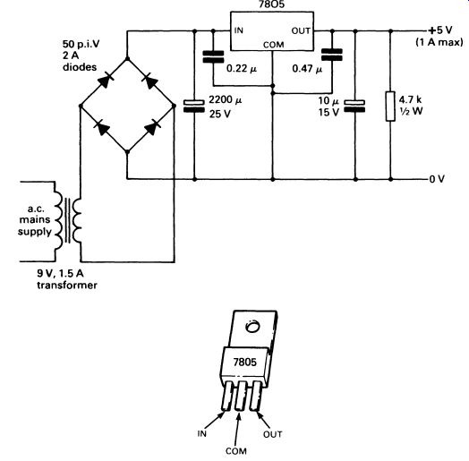
FIG. 3 a power supply for operating more complex TTL logic systems
A TTL system can impose very heavy instantaneous loads on a power supply. This can in turn result in interference 'spikes' in the power lines, upsetting the normal working of parts of the system. A cure can usually be effected by connecting small capacitors directly across the power lines, as near as possible to the ICs themselves. Usually 0.1 uF ceramic capacitors are recommended, but 10 uF, 15 V tantalum 'bead' capacitors can some times prove even better. Whichever type is used, about one capacitor per five ICs seems to work well.
Unused inputs It is important to ensure that unused inputs of TTL gates are connected, either to used inputs (but remember the fan-out limit of the preceding device), to the positive supply, or to supply 0V. Connections to 5 V should be made through a 1 k resistor; you can connect several inputs to the same resistor. Failure to terminate unused inputs may lead to the gate oscillating, harmful because it may cause the circuit to overheat.
Encapsulations
Although many encapsulations are listed by the makers, the DIL package (dual-in-line) is practically universal. A 14-pin DIL package is illustrated in Fig. 4. The pins are always numbered from pin 1, which is marked with a notch, or is the pin to the left of a notch in the end of the package, with the notch to the top. The pin numbers run in an anticlockwise direction, looking at the top of the package (which is held 'legs down'). The DIL package is usually made of plastic, though some high-quality devices may have ceramic packages, which are much more expensive.
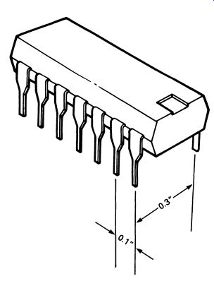
FIG. 4 a 14-pin DlL package
Schottky TIL TTL circuits are being improved continually, and a major advance has been in the introduction of a range of low-power Schottky ITL circuits. They use the same code numbers as the standard series, but with 'LS' before the type code--e.g. SN74LS00. Operating speeds are about twice as high, and power consumption is as low as one-fifth of that of standard TTL. The only 'minus' is the cost, about 20-30 percent more than the standard range.
Mainly because of the much reduced power consumption, the Schottky TTL is now more widely used than the standard TTL. In any digital system, and particularly in a large one, power supplies represent an appreciable fraction of the total cost, and the savings that can be made here will more than pay for the higher cost of the 'LS' series circuits. Indeed, it is the problem of power supplies that has been an important factor in the rapid growth and acceptance of the other major logic family, CMOS.
2. CMOS
Whereas TTL ICs are based on the bipolar junction transistor, CMOS ICs are based on the field-effect transistor. Fig. 5 illustrates a CMOS 2-input NAND gate. Before looking at the way this circuit operates, bear one fact in mind: the MOSFET is a voltage-operated device, and the gate insulation means that, for all practical purposes, there is no gate current. It is this that enables CMOS ICs to achieve astonishing power economies.
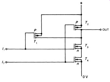
FIG. 5. A 2-input NAND gate using CMOS technology
Clearly, therefore, the inputs for the NAND gate in Fig. 5 will take no current. If the output is feeding another CMOS gate, then the output will not be required to deliver any current! The operation of the gate shown in Fig. 5 is as follows. Consider the circuit with both inputs taken low (logic 0). With / 1 low, T3 will be off (high resistance) and T1 will be on. With /2 low, T4 will be off, and T2 will be on. This much should be quite clear--if it is less than clear, you should re-read Section 9. The output terminal is held at a high potential (logic 1) via T1 and T2.
Now let us take / 1 to logic 1. This will switch on T3 and switch off Tt. but the output will remain at logic I because T2 is still on and T4 is still off. The same thing happens if / 2 and not I 1 is taken to logic 1. If, however, both inputs are at logic 1, then T1 and T2 are both off, isolating the output from the positive supply, whereas T3 and T4 are both on, making the output logic 0. Obviously, the simple circuit of Fig. 5 functions effectively as a NAND gate. It is a characteristic of CMOS that most power is used during the transition from one state to another, so the average power required is a function of the switching frequency. Typically, a NAND gate like the one in Fig. 5 would use less tha 0.11 uA with a 5 V supply when working! CMOS has some other advantages. It can be used with a wide range of power-supply voltages-the RCA 'B' range, for example, works from 3 to 18 V. Because of the lack of any appreciable voltage drop across the IGFETs when they are turned on, the logic 1 and logic 0 outputs are very close to the power-supply voltages-only about 10m V below the + supply or above OV. CMOS logic also switches neatly at half the supply voltage.
For a 5 V supply, the output switches as the input crosses 2.5 V; for a 12 V supply this happens at 6 V; and so on.
Finally, CMOS has far greater immunity to power-supply 'noise' than TTL and will tolerate noise of at least 20 percent of the supply voltage without problems. Clearly, CMOS is the first choice for battery-operated equipment. A complex CMOS system can be run from a small 9 V battery, and the battery will have a very long life; the voltage can drop to below 6 V before the circuits are affected adversely. No power supply or smoothing circuits are generally required, though a small (10 uf or so) capacitor is often connected across the battery. In general, power-supply decoupling capacitors such as tend to be sprinkled liberally around TTL circuits are not needed for CMOS. But there are disadvantages, too. CMOS is slower than TTLs. A CMOS counter might typically work at up to 5 MH-quite quick, but only a tenth as fast as a corresponding TTL circuit. The available output current is also low. This is not, of course, a problem within a wholly CMOS system (fan-out of a CMOS gate is more than 50) but means that buffering circuits are generally needed to drive indicators or control relays. The output is equivalent to a series resistor of 400 ohm-1 k, so by Ohm's Law we can see that with a 10 V supply only a few milliamps can be taken from the output. In practice, the output current is further limited by the safe dissipation of the device, around 200mW per package (i.e. 50 mW per gate for a quad NAND gate like the CD4011).
Handling CMOS
As we saw in Section 9, the MOSFET is susceptible to damage from electrostatic voltages. The same is true of the CMOS IC, though the manufacturers build in various safety features. A CMOS input actually looks like Fig. 6. This protection system works for voltages up to 800 Y-4 kV depending on the device. But since your body can easily pick up a charge of 10 kV when you walk across a nylon carpet, precautions are still essential. A suitable bench top for working with CMOS is made of a conductive material and is earthed.
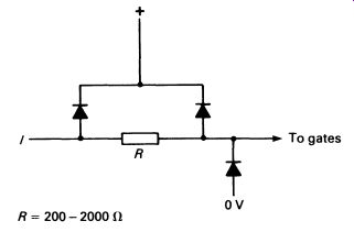
FIG. 6 typical protection circuit for CMOS inputs
High electrostatic potentials can also appear on the bit of a soldering iron. A rather inconvenient cure is to earth the bit (but not through the earth pin of the power socket). A better cure is to use a soldering iron with a ceramic shaft-the ceramic conducts heat from the element to the bit of the iron, but with very high electrical resistance and low capacitance.
The use of a ceramic-shafted soldering iron and earthed conductive bench top should provide sufficient electrostatic protection for all modem CMOS devices.
3. COMPARISON OF TIL AND CMOS
It is useful to compare the main characteristics of the two major logic families. The circuit designer will generally choose the logic system according to the design requirements-power supply (mains or battery?), operating speed, outputs required, and of course price.
Fig. 7 compares a simple gate-a quad-NAND gate in TTL (LS) and CMOS; and Fig. 8 compares a more complicated circuit-a 4-bit binary up/down counter.
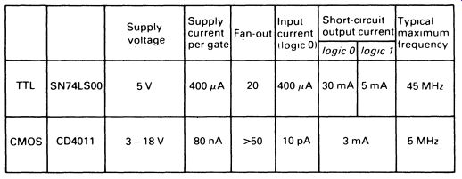
FIG. 7 comparing characteristics of similar simple TTL and CMOS
circuits --- Quad- NAND gate: comparison of characteristics; TTL and
CMOS
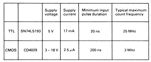
FIG. 8 comparing characteristics of similar complex TTL and CMOS
circuits ----- 4-bit binary up/down counter: comparison of characteristics;
TTL and CMOS
QUESTIONS
1. The output of a TTL gate is connected, via a meter that reads current, to the 0 V supply line. Suggest typical current readings when the output is at (i) logic 1, (ii) logic 0.
2. What are typical power-supply requirements for (i) TTL, (ii) CMOS?
3. Compare the TTL and CMOS logic families for the following characteristics: (i) current consumption from the supply, (ii) speed of operation, (iii) immunity from interference, (iv) tolerance of variations in the supply voltage.
4. What precautions need to be taken when handling CMOS circuits?
5. Which logic family would you use in designing a system for the following uses: (i) a stop-watch, (ii) high-speed data transfer system for a computer, (iii) control logic for electronic ignition system in a boiler?