BY ADOLPH A. MANGIERI
The basics of computer port operation and instructions for using them to expand computer flexibility.
FOR A microcomputer to "do something" truly useful, it must have input and output ports. The I/O ports make it possible for the computer to "interface" with practical devices-relays for appliance control, switches (or a keyboard) for feeding in desired commands, keyboard and video or hard-copy terminals for communicating with the computer, etc. Though 8080and Z80-based micros can control up to 256 I/O ports, few are equipped with more than two. In this article, therefore, we will describe how to add I/O facilities to expand a Z80 or 8080 computer's flexibility.
To add the I/O ports described here to any Z80 or 8080 micro, you must have a basic familiarity with port operation and addressing and bus structure. (This information is detailed in manuals that accompany the computers.) A few ICs will get your computer up and running.
Port examples presented here are for a Radio Shack TRS-80 Level I computer that uses the T-BUG monitor and a Level II computer with machine code and BASIC. You can use a solderless breadboard to perform experiments and to prototype circuits.
Port Basics. There are a number of different types of I/O ports in use. An elementary port may simply display information on a bank of LEDs, operate relays, or input data from a bank of switches. A complex port, on the other hand, can accommodate such sophisticated devices as an ASCII keyboard, full-graphics CRT monitor, and hard--copy terminal. Although all ports share the common computer bus, each is assigned a specific address and is provided with logic circuitry that enables the port only when it is addressed.
Machine-code instructions define CPU input and output operations. Two--byte instruction D3 XX initiates an output operation to a port. (D3 is the output instruction and the Xs indicate numbers for specific port addresses, such as D3 00, D3 01, D3 02, etc.) When a Z80 CPU fetches and executes this instruction, it generates an IOREO (I/O request) pulse and a WR (write) pulse, both active low, as indicated by the lines above them. These are logically added in an external AND gate and delivered as the OUT pulse on pin 21 of the TRS-80's bus. The data byte in the CPU accumulator register is placed on data bus lines DO through D7. Simultaneously, address byte XX is placed on address lines AO through A7.
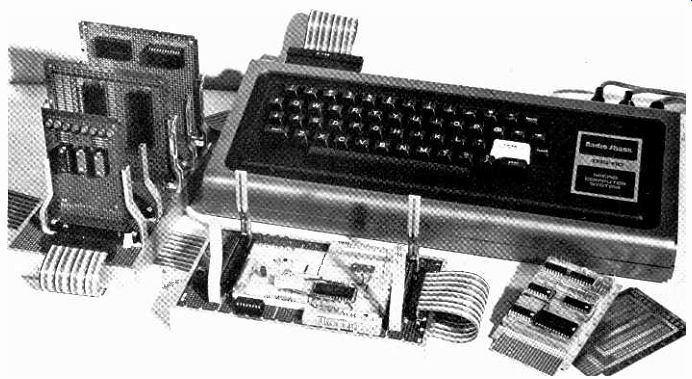
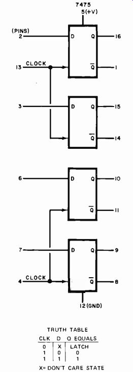
Fig. 1. Internal logic of 7475 (including pin-out) and truth table for
each latch.
Port-select logic constantly examines the OUT and address lines, waiting for the simultaneous appearance of the OUT pulse and port address. When this occurs, the port is enabled and data on the data bus lines enters the port. Address bytes can be from 00 to FF (hexidecimal) to allow up to 256 output ports to be used with suitable decoding.
Machine-code instructions DB XX (input instruction with port address) initiates an input operation from the selected input port. Here, IOREQ and RD (read) pulses are added in an external AND gate and delivered as the IN pulse on pin 19 of the TRS-80's bus.
Port logic detects the simultaneous appearance of the IN pulse and port address and enables the port. At this time, the port connects its output lines to the data bus and the CPU copies any data present on the bus into the accumulator register. After data acceptance, the port frees the data bus for other purposes.
The accumulator register is the source and destination of data with the D3 and DB instructions. The Z80 instruction set includes a number of special I/O instructions that effect data transfers to and from other registers and memory, with some instructions allowing movement of data in blocks.
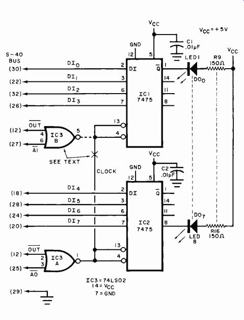
Fig. 2. Two 7475s and. a 74LS02 can be used to form an 8-bit port or,
with slight modifications, two 4-bit or four 2-bit ports.
Output and input ports can have the same address, such as output D301 and input DB 01. Port-select logic differentiates between the two by OUT and IN pulses. "Standard" or "isolated" I/O addressing allows up to 256 input and 256 output ports to be addressed by the computer. This is ample for just about any imaginable home computer system.
An alternative form of port addressing employs memory-mapped I/O. Each port, in effect, is addressed as memory.
This method allows thousands of ports to be addressed and affords some programming advantages.
Simple Output Port. Inexpensive 7475 TTL ICs can be used to make 2-, 4-, and 8-bit latching-type output ports.
As shown in the truth table in Fig. 1, data latch output Q follows input data D as long, as the clock (CLK) line is high.
When the CLK line goes low, data D is latched to output Q. The internal logic of the 7475, including pinout, is shown in Fig. 1. Note that each clock line drives two latches.
Two 7475's can be connected as an 8-bit Latching port (Fig. 2). LEDs connected to the Q outputs turn on when their respective data D input is high.
The port shown in Fig. 2 is addressed by instruction D3 00, which places binary 00000000 on lines A0 through A7.
The least-significant bit is on AO. When OUT and AO are true, the port is enabled by IC3A and the data byte held in the CPU accumulator register is displayed in binary on the LEDs. Address line bits Al through A7 are "don't cares," provided they are not assigned to other ports.
Hence, instruction D3 FE also selects this port because bit AO is low.
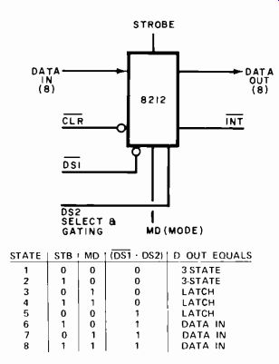
Fig. 3. The 8212, an 8-bit I/O port, and its truth table. This IC has
tri-state provisions. That is, in one mode it can be electrically isolated
from the system bus.
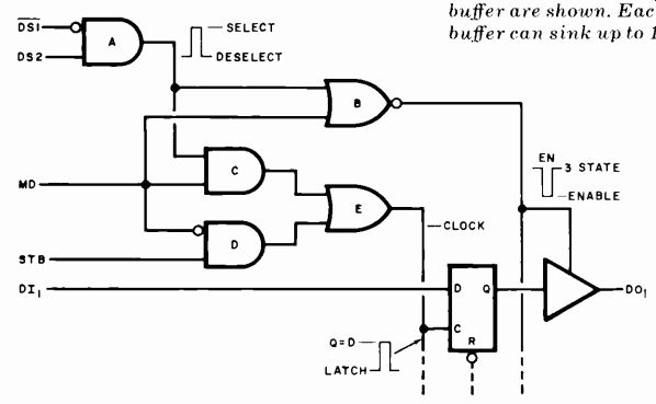
Fig. 4. A portion of the internal control logic of the 8212. Only one
of its eight latches and output buffer are shown. Each output buffer can
sink up to 15 mA.
Ports that do not require all eight data bits are easily arranged. To set up two 4--bit ports, break the clock line at X and add the second NOR gate (Fig. 2). Port IC1 is enabled by instruction D3 01, which places binary 00000001 on the address lines. The 0 bit on line Al causes selection of port IC1. You can also separate the four clock lines and arrange four 2-bit ports, using address lines A2 and A3 for port selection.
Progressive addressing allows up to eight input and output ports to be used.
One or more ports can be enabled by one instruction, simplifying programming and hardware requirements. Although it requires additional ICs in each port, full decoding of the address bits allows up to 256 input and output ports.
For example, the TRS-80 cassette port is fully decoded and selected by instruction D3 FF. For this and other reasons, the ports described here are assigned active-low address bits for selection. For an elementary example of both fully decoded port and memory-mapped port, refer to the TRS-80 Technical Reference Handbook.
Complex 110 Port. Intel's versatile 8212 I/O chip can be used as either a latching or a non-latching output port, input port, gated bus driver, or straight--through buffer, to name just a few of its applications. This high-speed Schottky TTL device includes eight data latches and output buffers that can be tri-stated (switched to high impedance). Each buffer can sink up to 15 mA. The function diagram of the 8212 is shown in Fig. 3, which also illustrates chip signals and the IC's truth table. A portion of the internal control logic and one of the latches and its output buffer are illustrated in Fig. 4. For simplicity, CPU-interrupt control logic, which controls interrupt output INT, is omitted.
Familiarity with the control logic simplifies application. Mode control line MD is tied low (logic 0 or ground) for the input-port mode and high (logic 1 or Vcc) for the output-port mode. Lines DS1 and DS2 are the device-select, or gating--control, lines. When DS1. DS2 is 1, the device is selected by a high at the output of gate A.
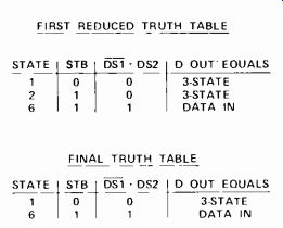
Fig. 5. Reduction of the truth table for the 8212.
The data-latch clock is strobed two ways. When line MD is low, gate C is defeated and strobe line STB passes a pulse through gates D and E to the clock line. When line MD is high, gate D is defeated and gate A passes a pulse through gates C and E to the clock line.
Similarly, the output buffers are also operated two ways. When line MD is high, gate B goes low and enables the buffers continuously. This is a necessary requirement for a latching-output port.
When line MD is low, the selected pulse from gate A passes through gate B to enable the buffers briefly, after which they return to tri-state. This is a necessary requirement for an input port.
The truth table is simple to use if you keep in mind the port or application requirements. To illustrate, let us implement an input port. In this case, MD must be tied low (grounded). Strike out all rows or states listing MD as 1 in the Fig. 3 truth table. Since MD is assigned, strike out column MD. We know from port basics that the input port must not latch onto the data bus. This eliminates state 5 and all that remain are states 1, 2, and 6, as shown in the reduced truth table in Fig. 5.
Clearly, state 6 must be retained for device selection and data transfer. Recalling that the STB line must be used to strobe the latches when line MD is 0, state 2 is deleted so that STB can alternate between 1 and 0. This results in the final truth table shown. Check this truth table to be sure it accomplishes the application's requirements. In this case, state 6 enables the port, placing port data on the data bus. State 1 "deselects" the port and tri-states the output buffers as required.
In the final step, computer pulses are assigned to DS1, DS2, and STB. Available computer pulses are IN and AO, the latter assigned to this port and active low. Notice that STB and DS2 are active high. With DS1 active low, connect IN to DS1. Pass AO through inverter IC6A and then to both STB and DS2 (Fig. 6). To use the 8212 as a latching output port, tie MD high (to VCC). Port requirements include device select with data in (state 7 or 8) and device deselect with latching (state 3 or 4). STB is a "don't care" line. Connect computer output pulse OUT to line DS1. Address line bit AO is inverted by IC7A and connected to line DS2 (Fig. 6). The LED is off when D is high. If this is objectionable, add inverting buffers between port outputs and light-emitting diodes.
For the 8212 to serve as a straight-through buffer or line driver, requirements are device select, data out equals data in, and continuously enabled output buffers. State 8 will effect these requirements. Connect line MD and DS2 to VCC and line DS1 to ground. For use as a bidirectional bus driver, interrupting ports, etc., see the Intel 8080 User's Manual.
Computer Hookup. The TRS-80 accepts a special 40-contact card edge connector. However, you can substitute a standard 44-contact card socket, such as a Vector No. R644-2, after modifying it. To do this, fit a thin piece of hard plastic into the connector slot to cover the two top and bottom contacts at one end of the connector. You now have a 44--contact connector that for all practical purposes has been modified to serve as a 40-contact connector.
Install the modified connector in the TRS-80, making sure that lateral play barely exceeds 1/64" (0.4 mm). Carefully remove the modified connector and cement the small plastic pieces solidly in place. Recheck connector fit before the cement sets. Then use a lettering kit to mark an UP label on the up side of the connector.
Solder a 12" to 18" (30.5 to 45.7 cm) length of color-coded 40-conductor ribbon cable, such as Vector's No. KW2-40, to the connector. Make a record of which conductor connects to and what signals are present on each pin.
Refer to the TRS-80 Technical Reference Manual or User's Manual for pin assignments.
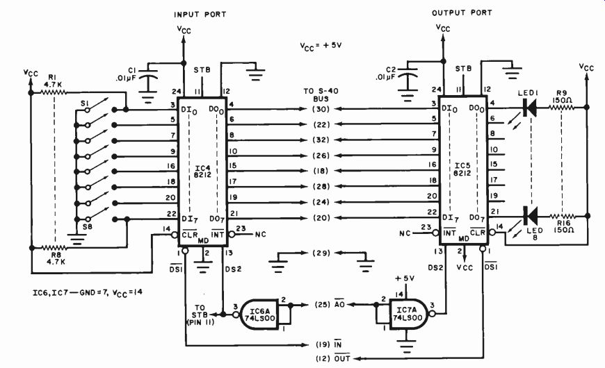
Fig. 6. An experimental I/O port using a pair of 8212s with switch inputs
and light-emitting diode outputs.
PARTS LIST
C1,C2--0.01-µF disc capacitor IC1.
C2-7475
IC3-74LS02NOR gate
IC4, IC5--8212 8-bit 1/O port
IC6,IC7-74LS00 low-power quad 2-input NAND gate
LED1 through LED8--Light emitting diode
R1 through R8--4700-ohm resistor
R9 through R16--150-ohm resistor
S1 through S8-Spst switch
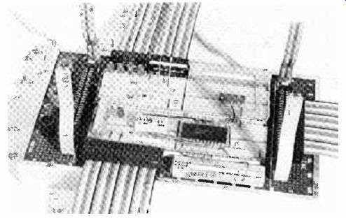
Fig. 7. Three computer links are provided on this patch-board using solderless
circuit connections.
Wire-Wrapping is used on connectors and under chassis.
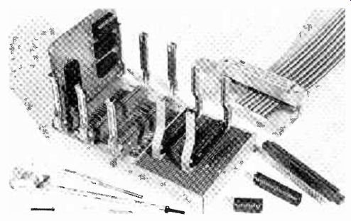
Fig. 8. Typical plug-in card chassis. Three large sockets are Vector
Electronics R644-3 with mating BR27-D card guides.
Smaller connectors are R644-2 with BR27 card guides.
Wire-forming and chiseling tools are also shown.
At this point, you can choose any of a number of conventional construction approaches. Perhaps the simplest is to use a solderless breadboard on which to experiment with the I/O port. A 40-pin IDC connector, such as a Vector No. KS2-40, can be fitted to the end of the cable, using a Vector No. P187 IDC fixture to make the connection. A mating connector can then be mounted on the solderless breadboard. Shown in Fig. 7 is this author's experimental setup, which includes wiring to a home-built card cage (Fig. 8) to support Wire Wrap circuit cards.
In Conclusion. From the foregoing, you can see that it is relatively simple to interface a computer with external devices to perform useful operations. You could conceivably use all 256 I/O ports to control everything in your home.
Source: (Popular Electronics Electronic Experimenter's Handbook (1982)
Also see:
Precision References for Current & Voltage
Listen To A New World Of Sounds With Ultrasonic Detector
Build a Dynamic Audio Noise Filter