AMAZON multi-meters discounts AMAZON oscilloscope discounts
Before servicing a watch, the watchmaker learns what makes the mechanism tick. Before diagnosing trouble in a human being, the physician spends many years learning how the body functions, for this knowledge is invaluable in the "troubleshooting" he must do later.
The radio technician must have some idea of how the transistor works in order to service transistor radios. This is probably more important than any other factor in reducing repair time, preventing callbacks, or just increasing his efficiency and professional reputation. This is why the first section is de voted to this subject.
BASIC TRANSISTOR FUNCTION
The basic purpose of the transistor is to control the flow of electrical current so that a signal is either produced, amplified, or changed in some manner. A transistor which produces a signal is called an oscillator. One which amplifies is simply an amplifier, although it may be further classified by the type of signal it amplifies, such as an audio-, IF-, or RF-amplifier.
We know that the function of a simple conductor such as a piece of wire is to provide the path for current in a circuit; and that the function of a nonconductor, or insulator, is to block current flow. The transistor allows a controlled amount of current to flow under certain conditions; it is therefore known as a semiconductor. The applied voltages, temperature, and circuit-resistor values, and the materials in the transistor itself, determine how much (or how little) conduction will take place.
One of the miraculous things about transistors is that they can do many of the same tasks a vacuum tube can do, but with much less effort. This means greater efficiency, lower operating voltages, less drain from the power source-all with a unit that is physically smaller than a vacuum tube.
Diode Action Is Basis for Transistor
The simple diode, which has long been used to detect or rectify signals, is the backbone of the fantastic transistor. A short review on how diodes work will help in understanding transistors.
Fig. 1-1. The pure crystal material - a perfect insulator in its original
form.
A typical modern diode may be made of germanium, silicon, or a similar material. These materials, in pure crystalline form (Fig. 1-1), make extremely good insulators; if no other materials were added, the diode would be unable to pass any current and would therefore be useless. However, the diode is actually divided into two sections ( di meaning two) and a certain amount of "impurity" added to each section. The impurity is simply a different type of material which supplies current carriers (Fig. 1-2) of either negative or positive polarity, de pending on the material added in the manufacturing process.
One type of impurity will produce N type carriers, which are negative; and another impurity will provide P type carriers, which are positive.
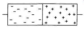
Fig. 1-2. Adding impurities to the crystal material produces charged carriers.
It is the presence of these free current carriers that allows the diode to become a fairly good conductor under the conditions shown in Fig. 1-3. When a battery is connected in the proper direction, the junction between the N and P sections are literally flooded with current carriers. This means the resistance of the diode to current flow is very low. The reason the diode allows current to pass is that there are plenty of free current carriers at the junction of the two diode sections.
To understand the principle of conduction through a diode more clearly, refer to Fig. 1-3 again. The negative battery terminal is connected to the N section of the diode, which contains free, movable electrons. Since like polarities repel each other, the negative field of the battery pushes the electrons toward the junction. Likewise, the positive pole of the battery repels the positive carriers toward the junction. It takes only a small voltage to give the charged carriers sufficient energy to cross the junction; and once they start moving, a constant exchange takes place. As negative carriers move into the P region, positive carriers cross into the N region (a fact which will become important later on). For the moment, however, the main thing to remember is that the negative carriers ( electrons) move through the diode and back into the battery. An ammeter placed in the circuit (Fig. 1-3) will indicate current is flowing.
The Nonconducting Diode
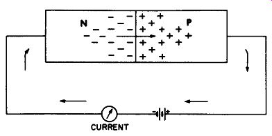
Fig. 1-3. Current will flow through the diode when a battery is connected
in the proper direction.
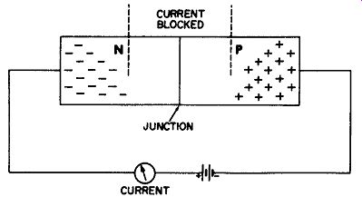
Fig. 1-4. Reversing the battery connections blocks the current through the
diode.
But let's suppose the same diode is connected to the same battery, except that the polarity is reversed as shown in Fig. 1-4. The negative electrons in the N section are now attracted by the charge at the positive terminal of the battery, and the positive current carriers in the P region are attracted by the charge at the negative terminal. The result is that both varieties of current carriers in the diode are pulled away from the junction, instead of toward it. This leaves no free carriers in the center of the diode; so this area again becomes an insulator, just as it was before the N- and P-forming materials were added to the pure crystal. The battery current is now blocked, and current flow ceases. Even if the battery voltage is in creased, practically no current will flow. We say "practically" because a very minute "leakage" current does exist because of heat or moisture.
Ohmmeter Causes Diode Action
When an ohmmeter is placed across a diode, the resistance shown will be low or very high, depending on which way the leads are connected. The reason is that the ohmmeter is really just a milliammeter connected in series with a battery.
(Fig. 1-5.) The negative lead of the ohmmeter in Fig. 1-5A is connected to the N side and the positive lead to the P side of the diode.
This forces N and P current carriers across the junction, creating a low internal resistance. Current from the ohmmeter battery can now flow through the circuit, and the meter indicates a fairly low resistance (usually under 1,000 ohms). This reading is actually a result of the current flow through the conducting diode and the meter, but the meter face is marked in ohms. In other words, a lower ohms reading indicates a greater current flow through the meter.
Now examine the circuit in Fig. 1-SB. The only difference between it and the one in Fig. 1-5A is that the ohmmeter has been turned so the positive lead is connected to the N side of the diode, and the negative lead to the P side. The polarity of the internal battery is such that the free current carriers are attracted away from the center of the diode. This creates an insulated area in the diode, making it void of all current carriers, both positive and negative. Battery current is now blocked; so nothing flows through the meter. The ohmmeter now reads a very high ohms value and theoretically would read infinite resistance, except that there is always a very slight leakage. This will be read as a high resistance value if the meter is sensitive enough.
So we have now proved that a diode can be made a high or a relative low resistance, depending on the polarity of the voltage connected to it. But what does this mean as far as a transistor is concerned? The answer will become evident very shortly.
(A) With negative terminal of ohm meter connected to N-type material. (B) With positive terminal of ohm meter connected to N-type material.
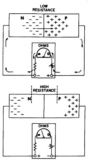
Fig. 1-5. Action of the carriers when an ohmmeter is connected across a
diode.
The NPN Transistor
A curious and interesting effect occurs when three instead of two diode sections are placed together. Fig. 1-6A shows a P-type section, containing free positive current carriers, positioned between two N-type sections. Actually, two diodes have been formed-diode 1 and diode 2, both using a common P section in the middle. The schematic symbol for this arrangement is shown at the right in Fig. 1-6B. The first question that arises is, "What happens when a battery is connected across this structure?" Fig. 1-7A shows the battery connected in one direction, and Fig. 1-7B shows it connected in the other direction. Note that in both examples, one of the diodes is biased in the high-resistance direction, causing free current carriers to be pulled away from the junction and thus leaving a blank area which blocks the flow of current. The reason is that the positive pole of the battery is always connected to one of the N sections, attracting minus carriers toward the outside edge and away from the junction.
This produces an insulated area.
(A) Equivalent diode structure. (B) Schematic symbol.
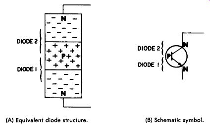
Fig. 1-6. The NPN transistor.
(A) Negative terminal connected to N material of diode 1. (B) Negative terminal connected to N material of diode 2.
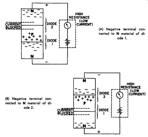
Fig. 1-7. Action of the carriers when a battery is connected across the
NPN structure.
If the battery and meter shown in Fig. 1-7 were both part of an ohmmeter, a similar action would take place. The cur- rent getting through the circuit would be quite small and the resistance would be fairly high. This is called the leakage resistance and is the basis for one of the transistor tests described in a later section.
The battery voltage in Fig. 1-7 can be increased to several volts and still very little current will flow. With increased battery voltage, however, there is a good source of current but the blocked area must be unblocked before it can flow.
The very simple method generally used to unblock the insulated area is the secret of transistor action.
(A) Action of the carriers. (B) Circuit configuration.
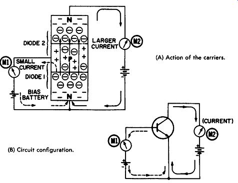
Fig. 1-8. Forward biasing the NPN transistor.
Adding "Forward" Bias
The easiest way to make current flow through an area where there are no free current carriers is to send some current carriers into the area. This is done very simply in Fig. 1-5A.
A small voltage is connected across diode 1. The battery is connected so the polarity is in the forward, or low-resistance, direction (negative pole connected to the N material, and positive pole to the P material). This causes negative carriers to be pushed upward and into the P area. Most of these carriers will travel on through the narrow P area and enter the formerly blocked area. Once the carriers have filled the upper N area, the larger battery keeps them moving into the output circuit, as indicated by the current flow in meter M2 in Fig. 1-8A. The electrons continue to flow through the larger battery and back into the bottom N region, their point of origin.
A very small current will also flow in the input circuit (see meter M1), but it is much less than the M2 current because the input voltage is less. The result is transistor current gain.
This circuit is shown using a transistor symbol in Fig. 1-8B. There are several reasons why this NPN transistor has gain:
1. The P area is made much narrower than the N areas, allowing negative carriers to cross it easily once they are started.
2. The negative carriers are easily pushed out of the bottom N area because the small battery is connected across diode 1 in the forward, or low-resistance, direction-the direction which makes current flow easily.
3. The output battery being larger than the input battery, is able to draw more current once the transistor has been unblocked by the smaller battery.
Variations of this circuit will be shown later, but this is the basic NPN circuit.
The PNP Transistor
The PNP transistor is similar to the NPN unit, except that the diode sections are arranged as shown in Fig. 1-9. An N section is sandwiched between two P sections, and the positive current carriers now become more important.
(A) Equivalent diode structure. (B) Schematic symbol.
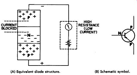
Fig. 1-9. The PNP transistor.
Again, regardless of which direction the battery is connected, one of the diodes will be biased in the high-resistance direction-that is, the positive carriers will be attracted away from the center, and battery current will be blocked. However, if a small battery is connected across diode 1 in the forward direction as shown in Fig. 1-10, that diode will start conducting slightly. (Notice that the positive battery terminal is connected to the P section and the negative terminal to the N section.) Even a small voltage in the forward direction will force positive current carriers out of the lower P section.
(A) Action of the carriers. (B) Circuit configuration.
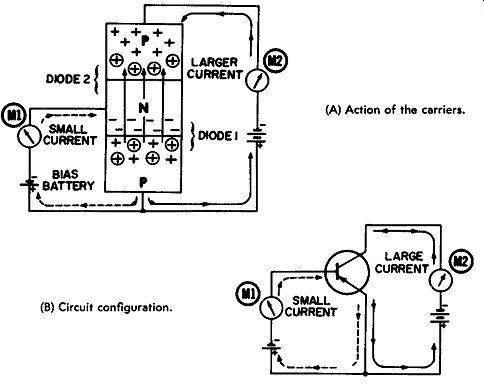
Fig. 1-10. Forward biasing the PNP transistor.
Most of the positive carriers pushed out of the lower P section travel upward and through the narrow N section. This means they will flood the upper P section and unblock the transistor. With current carriers available at all points in the transistor, the larger battery can now send its own current through the transistor and into the output circuit, as evidenced by meter M2.
As with the NPN transistor, the output current is larger than the input current because the voltage required in the input is extremely small. Since diode 1 is biased in the low resistance direction, carriers are easily sent upward from the lower P area, even though the small battery may be only 0.1 or 0.2 of a volt. These carriers unblock diode 2 so current from the larger battery can flow through.
Since the diode sections were reversed to make the PNP transistor, the batteries were also turned around when they were connected to the PNP transistor. This is the reason the arrows depicting input and output current are reversed; electrons always leave the negative pole of a battery and enter the positive pole. The arrows show electron flow from the batteries.
Although it will be varied slightly later, this is the basic PNP circuit.
IDENTIFYING THE TRANSISTOR ELEMENTS
The bottom section of the input diode is called the emitter because it emits current carriers, very much like the cathode of a tube emits electrons. The opposite end of the transistor, to which the output circuit is usually connected, is known as the collector because it collects the carriers which come out of the emitter; this simulates the plate of a tube. The middle section is known as the base because, in the manufacture of the transistor, it is usually made first, forming a base for the other two elements. The base in some ways acts like the grid in a vacuum tube, in that it controls the flow of current through the transistor.
In some schematics the emitter, base, and collector are labeled E, B, and C; in others, no letters are used. The emitter always has an arrow; the base is in the middle; and the collector is always at the end opposite the emitter, but contains no arrow.
When the emitter arrow points toward the base, the transistor is a PNP unit; when it points away from the base, it is an NPN unit.
TRANSISTOR TYPES
In working with transistor equipment, it is important to know what types of transistors are used in the various circuits.
Practically all transistors in commercial equipment today are junction types--a description of how they are constructed, not how they are used in the circuit.
Fig. 1-11 shows several typical transistors and some of the functions each might perform in the circuit. The cases which house the lower-power types are usually either small rectangles or cylinders, whereas high-power types are usually found in larger diamond-shaped or circular cases.
The transistor type will usually determine the amount of output current it will handle under no-signal conditions. This current is called idling, or DC static current, because it represents the DC current drain of the transistor at rest, with no signal applied.
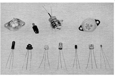
Fig. 1-11. Typical transistors.
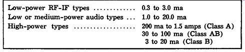
The values in Table 1-1 are not maximum current ratings but typical operating currents for amplifiers. Maximum ratings are seldom used in actual practice, except in some missile or similar application where it is important to get everything possible out of the transistor. Switching circuits, where the transistor is alternately turned on and off, can utilize maximum ratings because the unit is allowed to rest or cool during a portion of each cycle.
----------------- TABLE 1-1.
Typical DC Idling Currents
Low-power RF-IF types . . . . . . . . . . . . . 0.3 to 3.0 ma
Low or medium-power audio types . . . 1.0 to 20.0 ma
High-power types . . . . . . . . . . . . . . 200 ma to 1.5 amps
(Class A) 30 to 100 ma
( Class AB) 3 to 20 ma (Class B)
----------------------
Note in Table 1-2 that other important ratings are listed for transistors. These are maximum ratings, and do not represent typical circuit operating values. For example, the maximum ratings for power transistors are achieved by utilizing large heat sinks under special laboratory conditions, where the room temperature and other variables are carefully controlled.
Trying to operate the same transistors at these ratings on the workbench could damage them permanently.
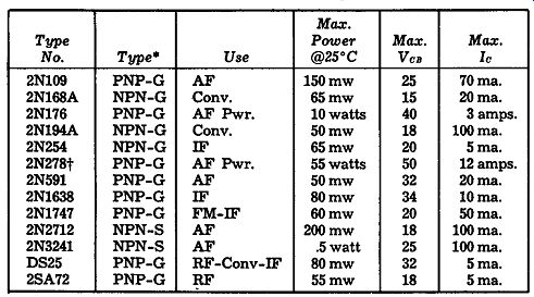
TABLE 1-2.
Absolute Maximum Ratings
G = Germanium
S = Silicon
Replaced by DS-501 for Auto Radios
To learn how to interpret this type of chart, let's see how the various ratings are applied. The 2N109 in Table 1-2, for example, is a PNP germanium transistor (PNP-G). Some transistors are made of silicon instead of germanium, and those are designated "S." The 2N109 is used as an audio-frequency amplifier (AF) , and has a maximum power dissipation rating of 150 milliwatts at room temperature (25° C). The voltage between collector and base (V c8 ) must never exceed 25 volts, and the maximum current (I_e) rating is 70 milliamperes. This was one of the early audio amplifiers, but was typical of the many similar audio transistors which were developed later.
Transistors are seldom operated near their maximum ratings.
For example, a typical collector voltage for the 2N109 when operating in most circuits would be 5-10 volts, instead of maximum rated voltage of 25 volts. The typical operating current would be about 1 milliampere, even though the maximum rating is shown as 70 ma. in the table.
Note that some transistors are only recommended for audio frequency applications (AF), while others are called out for higher-frequency applications in radios (IF, converter, RF, etc.). Some rating tables list the actual frequency cut-off point in megacycles. This is the point where the gain of the transistor begins to decrease noticeably when used in a particular type of circuit, and the radio would be weak if the transistor were operated at higher frequencies.
Audio power transistors have much higher ratings than the smaller transistors, as can be seen by examining the 2N176 and 2N278 ratings in Table 1-2. Nevertheless, the same general rules hold true: in typical amplifier circuits, the maximum ratings are seldom used. Power transistors in audio-output stages seldom have more than 12 volts applied between emitter and collector, and they operate at approximately one ampere DC or less. The 2N176 would probably draw 400 to 500 milli amperes in a typical Class-A circuit, whereas the 2N278 or DS501 would draw about one ampere of collector current.
One reason for never operating transistors too near their maximum voltage ratings is that there will be audio-voltage peaks or "spikes" when an audio input signal is applied.
This is especially true in the audio-output stage, where the signal has been amplified many times before it reaches that stage. The DC voltage supplied by the battery, plus the audio signal voltage, must never exceed the maximum rating of the transistor.