AMAZON multi-meters discounts AMAZON oscilloscope discounts
Circuit components such as coils, transformers, resistors, and capacitors are just as important to transistor as they are to vacuum-tube circuit operation. In fact, without coils or transformers, no signal could be tuned in or coupled from one circuit to another. Without resistors, voltages could not be stepped down and the current might exceed the transistor ratings. If capacitors were omitted, most circuits would become so unstable that oscillations, whistles, motorboating, and other noises would have a heyday.
It is a known fact that transistors generally do not fail as often as tubes. This places more importance on the other circuit components used with transistors. Instead of immediately suspecting a transistor when equipment failure occurs, we should ask ourselves, "I wonder if something has happened to one of the circuit components which is preventing a transistor from working properly?" Then, if checks indicate that the supporting components and connections are functioning as they are supposed to, the transistor itself can be suspected.
Note that this is exactly opposite from the approach used in working with vacuum-tube equipment.
So, before we can quickly analyze the circuit in order to tell whether it is functioning properly, we must thoroughly understand the role of each component. In other words, the whole is only as good as its individual parts. So the parts will be our next subject of study.
The various components will be placed into our basic circuit, one at a time; then their effect on the circuit will be studied.
BASIC CIRCUIT LIMITATIONS
The basic transistor circuits in Fig. 2-1 must be modified somewhat to make them useful and safe for the transistor.
Without some form of current protection, the transistor current would tend to "run away," and may go far enough to ruin the transistors. The components which prevent this are known as stabilizers or protection resistors.
After the transistor current has been set and stabilized at the proper point (depending on the type of transistor), some method of adding the signal into the transistor circuit must be employed so it can be amplified.
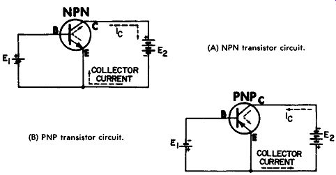
(A) NPN transistor circuit. (B) PNP transistor circuit.
Fig. 2-1. The basic transistor circuits.
Stabilizing Resistors
We know that the collector current (I_e) in Fig. 2-1 follows the path shown by the dotted lines. The amount of current which will flow for any given transistor depends on:
1. The amount of bias voltage E1 (usually 0.1 to 0.3 volt).
2. The temperature inside the transistor.
3. The amount of voltage in collector battery E2 ( usually 3 to 12 volts).
The third item, collector voltage, has the least effect of all the variables. Temperature and bias voltage have the most effect; therefore, they must be carefully controlled.
Both bias voltage and temperature, when increased, produce a greater collector current. That is, when E1 is increased, collector current will also increase; and when the temperature inside the transistor is increased, the collector current will again rise. So the thing which tells us we have too much bias voltage or too hot a temperature for our transistor is the collector current flowing in the output circuit. Any increase in collector current le above the normal operating point must be discouraged. The circuit components that check an increase in collector current are the stabilizers, which we are now going to discuss.
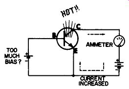
Fig. 2-2. Excessive collector current can ruin a transistor.
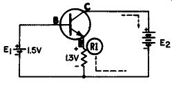
Fig. 2-3. A resistor in the emitter lead helps stabilize the collector current.
It is not practical to insert a meter in the output circuit of every stage and watch for excessive current, as shown in Fig. 2-2. However, we know that current flow in a circuit produces a voltage drop across any resistance inserted into the circuit. For instance, resistor R1 in Fig. 2-3 has been added in series with the transistor emitter. The path of collector current is then through the resistor, transistor, and battery, as shown by the dotted lines. Since it takes energy for the electrons to travel through resistor R1, a voltage drop appears across the resistor. The greater the current, the larger the voltage drop. (An easy way to remember the polarity of the voltage drop is that the resistor is always negative at the end where the electrons enter.)
We now have a measuring stick for collector current: The greater the current, the greater the number of electrons which try to "push" their way through the resistor, and therefore, the greater the voltage drop across resistor R1. Note the effect of this voltage drop in Fig. 2-3. Let's assume that 1.3 volts are dropped across R1, and also that the bias battery has a value of 1.5 volts. Now, what is the actual bias voltage between the base and emitter of the transistor? It is 1.5 volts minus 1.3 volts, or 0.2 volt. The 1.3 volts across R1 actually bucks the voltage from battery E1 and must therefore be subtracted from it.
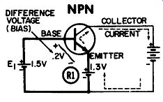
Fig. 2-4. Equivalent circuit of Fig. 2-3.
The equivalent circuit is shown in Fig. 2-4. The voltage produced across R1 is shown as a battery; this is the way it actually appears to the transistor. Remember, however, that the voltage at R1 is not a battery voltage source, since the 1.3 volts change as the collector current changes. For example, if the collector current increases, the voltages at R1 will also increase, maybe even to 1.4 volts. This would leave only 0.1 volt of bias, which would tend to "cool" the transistor and thus prevent any further increase in collector current. This is what is meant by collector-current stabilization.
Another way of stating it is this--as the collector current increases, the transistor temperature may also rise. But the increased collector current also produces, at R1, a greater "bucking" voltage which prevents further increases in current. This voltage also prevents a further increase in tempera ture by slowing down the flow of current through the transistor.
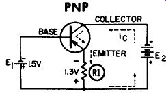
Fig. 2-5. Current flow through basic PNP transistor circuit.
Next, refer to the PNP circuit in Fig. 2-5. Stabilization resistor R1 has been added. The only difference between this circuit and the one in Fig. 2-3 is that the battery polarities are reversed, because of the PNP transistor connections. Electrons in Fig. 2-5 now flow out of the negative terminal of E2, down through the transistor, through R1, and back into E2, as shown by the dotted lines.
This means the polarity of the voltage produced across R1 is reversed, now being negative at the top and positive at the bottom. However, this voltage still bucks the one from battery E1 because the positive end of E1 is connected to the positive end of R1. The net result is that the actual voltage measured between base and emitter is still only 0.2 volt. This is clearly illustrated in the equivalent circuit in Fig. 2-6.
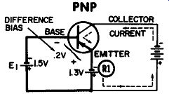
Fig. 2-6. Equivalent circuit of Fig. 2-5.
As the collector current and the temperature try to increase, the increased current produces, across R1, a greater "bucking" voltage which reduces the 0.2 volt to a smaller net voltage, preventing any further increase. The PNP transistor is, there fore, current- and temperature-stabilized.
Other Stabilizing Tricks
A resistor in the emitter lead is the most widely used "stabilizer" because it is such a simple and efficient way to control the collector current at very little cost. But it is not the only method.
Some circuits also use a resistor in the collector lead (R2 in Fig. 2-7) . Since the collector current also flows through this resistor, a voltage will be developed across it, in proportion to the amount of collector current flowing through it-the greater the current, the more the voltage drop. As a result, the voltage at the collector of the transistor is automatically adjusted with changes in current flow. A change in the collector voltage does not have too much effect on the collector current, although it does help control the voltage to some extent. The collector resistor is very seldom used by itself, however; circuits which use it will probably also have an emitter resistor.
The collector resistor (R2) has another advantage. We some times find RF voltages floating around in the lead between the output circuit and the battery. This can cause oscillations and unwanted noises in a radio. Increasing the resistance in that lead makes these unwanted signals easier to capture and "shunt" to ground before they can reach the battery. This is the purpose of the bypass capacitor shown in dotted lines across resistor R2 in Fig. 2-7. This is often called a decoupling network.
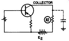
Fig. 2-7. A resistor in the collector lead will provide even better collector-current
stability.
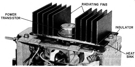
Fig. 2-8. Typical power transistor and heat sink used in an auto radio.
Another type of stabilizer is the heat sink (Fig. 2-8) or convector found in many high-power transistor circuits. The power transistor mounts on the heat sink, which is usually aluminum; the heat from the transistor flows into the metal and is then dissipated into the air. The heat sink thus prevents the concentrated heat from remaining in the transistor and destroying it. Also, since the flow of current through the transistor depends to a great extent on how hot the transistor is, the heat sink helps to keep the collector current at a safe value. Small transistors generally do not require heat sinks because their current and power requirements are usually very small, compared to the mode of operation of a power transistor.
Still another form of stabilizer, called a thermistor, is some times inserted in the base lead of a transistor circuit. The thermistor is a resistance which varies with temperature. (Its operation will be discussed later.)
ELIMINATING THE BIAS BATTERY
In early radios, old-timers will remember that three separate batteries were used-one for the filaments ( called the A battery), one for the plate supply (called the B battery), and the third for grid bias ( the C battery) . In transistor circuits, the A battery is automatically eliminated because a transistor has no filament. The B battery, in the collector circuit of the transistor, is usually of a much smaller voltage than the B supply in most vacuum-tube circuits. The C battery is in the base circuit. As with the tube, we would like to eliminate this battery if at all possible.
Biasing By Voltage Divider
We know that a voltage source, such as a battery, is needed in the collector circuit of the transistor. So the ideal situation would be to tap some voltage from that battery and use it for the base-voltage requirements. But since actual battery taps are not practical, another method is generally used.
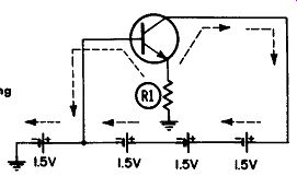
Fig. 2-9. A poor method of obtaining bias voltage.
If several small batteries are connected in series, several voltages can be obtained by connecting between them. An example of this is shown in Fig. 2-9, where four 1.5-volt cells are connected in series to provide 6 volts for the collector. If the base happens to require exactly 1.5 volts, such a system might be used. But it is usually not too practical for several reasons. For one thing, the chances are pretty slim that the transistor will need exactly that voltage on the base. Besides, other transistors in the radio will also need some form of bias, each of a different voltage. But even if all base leads could be tied into that point, there is still a disadvantage: One battery would have more current passing through it than the others.
There is one very simple method of getting exactly the right voltage for each transistor in the radio without using any extra batteries. In Fig. 2-10A, we see a 6-volt battery supply with a resistor connected across it. This resistor has several taps where different voltages are obtained. The midway tap has 3 volts on it because the resistance from there to the negative terminal is the same as it is to the positive terminal. The battery current will therefore produce the same voltage--3 volts--across each half.
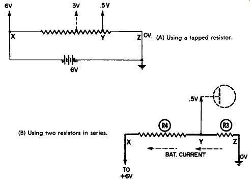
Fig. 2-10. Obtaining bias voltage from divider network. (A) Using a tapped
resistor. (B) Using two resistors in series.
By putting a tap near the ground end, we can obtain smaller voltages. For example, note that a tap is connected at the 0.5-volt point. Suppose we had a transistor circuit that required 0.5 volt on the base. The base could be connected near that point on the resistor, and the resistance measured between points x and y and y and z. The same resistance could be obtained from two fixed resistors (R3 and R4 in Fig. 2-10B). They could then be placed across the battery, instead of using the tapped resistor.
The resistance of R3 in Fig. 2-10B is much lower than that of R4, meaning that point y is electrically much closer to ground than to +6 volts. This is why there is only 0.5 volt at point y. In other words, as the battery current flows through R3 and R4, a much smaller voltage is produced, or "dropped," across little R3. So only 0.5 volt is found across R3; the balance of 5.5 volts is across R4 (measured between points x and y).
Connecting the Voltage Divider in a Circuit
We are now ready to connect the voltage divider into our transistor circuit. Remember that we are using the divider to replace the extra bias battery (the so-called C battery). In Fig. 2-llA the voltage divider is connected into the stabilized transistor circuit previously studied. The same circuit using battery bias is shown in Fig. 2-11B. By the addition of two simple resistors, R3 and R4, we have eliminated the necessity of an extra battery for base voltage. R3 and R4 are merely connected across the 6-volt battery, and the point between them is connected to the transistor base.
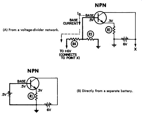
Fig. 2-11. Obtaining the bias voltage for an NPN transistor circuit. (A)
From a voltage-divider network. (B) Directly from a separate battery.
When the voltage divider is actually connected into the transistor circuit (Fig. 2-11A), the 0.5 volt may change slightly.
The reason is that the transistor will probably draw a small base current, which will have to flow through part of the voltage divider in the base circuit. For example, if some electrons from the transistor flow into the base lead (see the arrows in Fig. 2-11A), they will also flow through R4, toward the positive 6-volt battery terminal. This will cause a greater voltage drop across R4, and thus leave a little less voltage across R3. The values of R3 and R4 are calculated so the desired base voltage is produced when the transistor is connected to the voltage divider. These values depend on the transistor and how it is used. Some circuits even use a variable control to adjust the bias-but only when absolutely necessary, because a potentiometer costs considerably more than a fixed resistor.
The Voltage Divider in a PNP Circuit
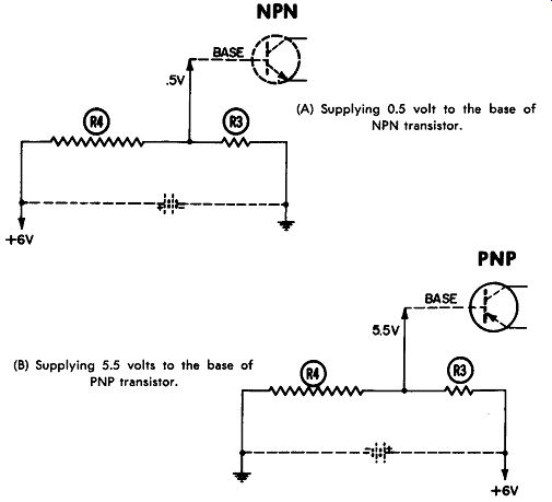
(A) Supplying 0.5 volt to the base of NPN transistor. (B) Supplying 5.5
volts to the base of PNP transistor. Fig. 2-12. Re-proportioning the voltage
division across the divider network by reversing the battery connections.
The same general principles can be applied to PNP circuits.
In the PNP transistor, however, the voltage required for the base is slightly less than the most positive voltage in the circuit. This means if a 6-volt battery is used in the output circuit, the base voltage will usually be a little less than 6 volts (such as 5.5 volts, for example). In Fig. 2-12, the base voltage for the PNP transistor is increased by turning the battery around. This puts the connection between resistors R3 and R4 at approximately 5.5 volts, because R3 has a much smaller resistance than R4. The exact base voltage, of course, can be varied for different transistors by using different values for R3 and R4. The new battery polarity is no problem because the collector battery is reversed in PNP circuits anyway.
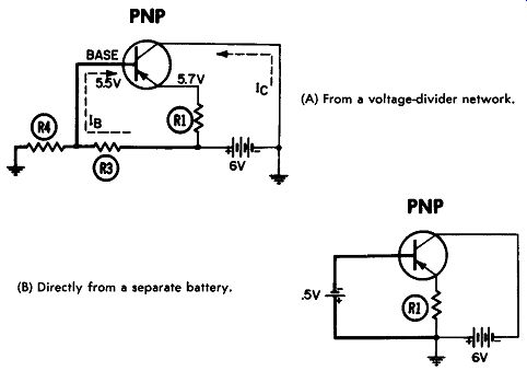
Fig. 2-13. Obtaining the bias voltage for a PNP transistor circuit. (A)
From a voltage-divider network. (B) Directly from a separate battery.
Now let's connect the emitter and collector leads to complete the PNP circuit. This is done in Fig. 2-13A. Resistors R3 and R4 are connected across the 6-volt battery, but since R3 has the lesser resistance, the base voltage is fairly high. An easy way to see why it is relatively high is to think of the base-lead connection as a movable tap across resistors R3 and R4. As the base tap is moved to the right, it gets closer to the positive pole of the battery and so the voltage goes up.
The circuit in Fig. 2-13B looks much like the NPN circuit in Fig. 2-11B, except for one major change. The battery polarity is now reversed, so the negative terminal is connected to the collector lead, and the positive terminal to the emitter lead through resistor R1. The positive terminal also is connected to the base lead through resistor R3, making the base and emitter voltages more positive in the PNP circuit.
Summary of Biasing Action
Small currents in the base circuit are amplified by the transistor, producing a much larger current in the output ( collector) circuit. The small current is started by applying to the base a voltage slightly different from the one on the emitter. This difference of potential produces an electric field which exerts a force or pull on the carriers in the emitter element of the transistor. The transistor then conducts, causing current to flow in the output circuit. This DC collector current (usually labeled le; see the arrows in Fig. 2-13A) does very little good, however, unless we have some way of utilizing it.
In other words, after the DC idling conditions have been set up, a method must be provided for inserting a signal into the input circuit, as well as capturing the amplified signal in the output circuit.
THE INPUT AND OUTPUT TRANSFORMERS
When injected in the base circuit, the signal will be added to the forward bias on one half-cycle and subtracted from it during the other half-cycle. When the signal is added, the output (collector) current will rise; and during the other half cycle, it will drop.
To explain how the signal becomes larger in the output circuit, we will cite an example. Suppose the DC bias is adjusted so that 1 milliampere flows in the collector circuit, as shown in Fig. 2-14. If the transistor has a DC current gain of 10 ( a very conservative figure) , our base current would be 0.1 milliampere. (This would be the steady value of current before any signal is applied.) Assuming the maximum amount of signal were added before clipping occurs, the base current would then swing from 0.1 to 0.2 milliampere. In other words, the signal voltage would swing the base current to twice its idling value for a 100% increase, and then down to zero for a 100% decrease.
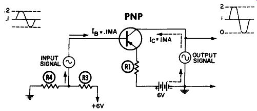
Fig. 2-14. How amplification is accomplished in a transistor circuit.
The collector current will also try to increase and decrease by about the same percentage. But a 100% increase in 1 ma makes the current go to 2 ma; and a decrease by the same amount will make it dip from 1 ma to zero. So, although both the output and the input currents change by the same percentage, the output signal is larger because it had a larger DC value in the beginning. In other words, there was a signal gain in this stage.
Probably the most efficient method of inserting the signal into the DC circuit is by a transformer, as shown in Fig. 2-15.
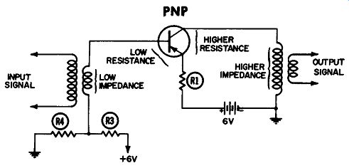
Fig. 2-15. Transformer method of coupling input signal to transistor stage.
The reason is that the transformer also can be used as a matching device.
The input diode of the transistor normally has a very low resistance because
it is biased in the forward (low-resistance) direction. On the other hand,
the collector diode usually has a higher internal resistance. For maximum
transfer of energy from the input transformer to the input of the transistor,
a low-impedance winding is therefore desirable.
For maximum energy transfer from the transistor output to the output load, a transformer which matches the transistor output impedance is desirable. The latter can be taken care of by using fewer turns in the base and more in the collector winding of the transformer.
Simple resistance coupling is more economical and, for this reason, is sometimes used despite a sacrifice in efficiency.
Direct coupling, where an element of one transistor is connected to an element of the following transistor, is also used in some circuits. However, coupling by transformer is still the most popular.
After forming our basic DC circuits in the first section, we later found it necessary to add certain resistors to prevent the transistor from being ruined by excessive heating. Specifically, we added a stabilizing resistor in series with the emitter lead, explaining that sometimes one is also used in series with the collector lead. The latter resistor prevents excessive collector current, and therefore, excessive heating of the transistor.
Resistors, in the form of a voltage divider, were also added in the base circuit. By adjusting the resistor values, it was possible to obtain any desired base voltage, which in turn produced the proper bias and transistor collector current. This eliminated the necessity for a C battery in the base circuit.
Although these resistors serve the very important functions of setting up and controlling the DC or idling conditions, they actually become somewhat of an obstacle for the signal when it is coupled into the stage. This can be easily understood if one point is remembered: the signal merely causes fluctuations in the DC idling current which was flowing before any signal was added. Then doesn't it stand to reason that if the idling current produces certain voltage drops across the resistors in the circuit, the signal current will also produce voltage drops across the resistors? In other words, as the signal tries to increase the idling current, the voltage drops will also increase, and vice versa.
Let's take an example. Fig. 2-16 shows the basic NPN transistor amplifier circuit, with stabilizing resistor R1, collector resistor R2, and bias resistors R3 and R4. Also shown (by arrows) are the paths taken by the base- and collector-current electrons. Now what happens when the signal is fed in across the input transformer? During one half-cycle (the positive half here), the base current will go up because the signal voltage increases the base bias. As the base current rises, so does the drop across resistors R4 and R1 in the base-current path.
This causes an increase in the voltage drop across these resistors. If these voltage drops are considered as small batteries placed in the circuit, will they oppose the input signal voltage or add to it? They will oppose, or buck, the signal and thus cause a loss of signal voltage reaching the transistor.
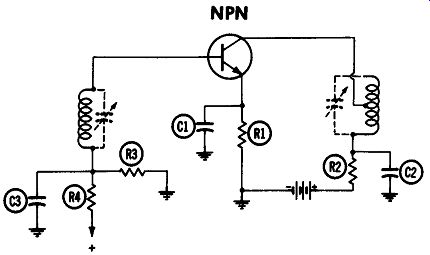
Fig. 2-17. Using bypass capacitors to prevent degeneration.
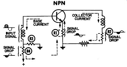
Fig.
2-16. Points where degeneration occur in the basic NPN transistor circuit.
The same is true of the resistors in the path of the collector current. Remember,
however, that collector current also flows through R1. So R1 actually gets
a double dose of voltage drop--most of which is caused by the collector current,
since it is much larger than the base current. This effect is sometimes referred
to as signal degeneration, or simply degeneration.
How is degeneration combated? One way is by adding by pass capacitors across the points of signal drop. This has been done in Fig. 2-17. The capacitors are large enough to hold their charge so the signal does not produce any voltage drop across the resistors. The voltage drops established by the DC idling currents are held steady. Another way of stating this is to say the signal is "bypassed" around the resistors. This lets all the signal be applied between the transistor base and emitter, where it can be amplified without getting lost in the circuit resistors.
These capacitors serve another useful purpose: they prevent stray signals from floating around in the various leads. These wandering signals could easily cause oscillations, resulting in unwanted whistles, motorboating, or squeals.
A TYPICAL AMPLIFIER STAGE
The circuit just covered (Fig. 2-17) is a typical amplifier stage. If it is to amplify RF or IF signals, the coupling trans-formers in the input and output circuits will be RF or IF tuned circuits. The circuits will probably use capacitors to tune them to the proper frequency ( as shown in dotted lines) , and possibly, adjustable iron cores or slugs. When tuned to a specific frequency, these coils become a very high impedance as parallel tuned circuits at resonance. It may therefore be necessary to tap down on the coil for the collector lead ( as shown in Fig. 2-17) in order to match the moderate output impedance of the transistor.
If the untuned input and output transformers were used in the circuit in Fig. 2-17, it would resemble an audio-amplifier stage.
Capacitor and resistor values will vary, depending on the type of transistor, the frequency of the signal being amplified (RF, IF, or audio), and the battery voltage. This circuit could be turned into a PNP one by simply changing the transistor and reversing the battery. If the new transistor has different ratings from those of the NPN transistor, there may have to be some component value changes, too, of course.
Adding Variable Bias (AGC) to Amplifiers
When the bias on an amplifier stage is changed automatically as the strength of the incoming signal changes, we call this AGC (automatic gain control). There is really no mystery about AGC. It is indeed very simple. Assume we want to apply AGC to our sample amplifier circuit. All we have to do is find some way of changing either the base or the emitter voltage as the strength of the incoming signal changes. One way is shown in Fig. 2-18.
Fig. 2-17 differs from Fig. 2-18 in one respect: instead of being tied directly to ground, R3 in the base circuit goes through the volume control first. This causes the base bias to change in step with the signal strength because the DC voltage across the volume control also changes.
As the signal gets stronger, a larger voltage is developed across the IF output coil. This causes the detector diode to con duct harder and thereby send more current through the volume control. The diode can conduct in only one direction; so electrons are sent down through the volume control. This current flow produces a negative voltage at the top of the volume control, which is connected to resistor R3. As a result, the base voltage becomes less positive. (It will probably never go negative because the voltage at the bottom of resistor R4 keeps it positive.) Strong stations will cause the base voltage to dip and thus adjust the bias on the transistor to the strength of each incoming signal.
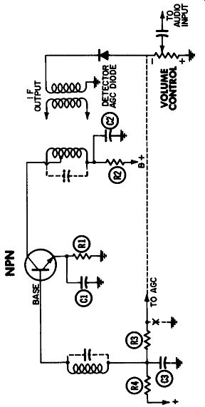
Fig. 2-18. An AGC-controlled transistor circuit.
The volume control is not always used for the source of AGC voltage (although it is a convenient point). In some circuits, a separate AGC resistor and diode are employed.
AGC can be applied to PNP amplifiers in a similar manner.
It is sometimes connected to the emitter instead of the base circuit. The major reasons for the AGC system are to prevent overloading and distortion on strong signals, as well as excessive signal fading.
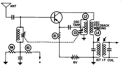
Fig. 2-19. A transistor oscillator circuit.
FEEDBACK FOR OSCILLATORS
It is sometimes necessary to make a stage oscillate. This is true in converter circuits, where a signal is needed which will combine with the one from the incoming station to produce the IF signal. This is the function of an oscillator-to produce an AC signal.
In Fig. 2-19, two items have been added to our basic transistor circuit-oscillator coil L3 and feedback winding L4.
Otherwise, it is almost identical to an amplifier circuit.
When the battery is connected, the first surge of collector current shocks oscillator tank circuit L3-C3 into the normal flywheel type of oscillation. The oscillations are replenished during each cycle by regenerations ( this is the purpose of the feedback winding) . Some of the oscillator-coil voltage is thus coupled back into the input circuit in phase, in order to give the oscillator tank circuit a boost of replenishing energy exactly when needed. The feedback coil may be in either the base or emitter lead, as in Fig. 2-19. Nevertheless, the feed-back voltage gets into the input circuit, between the base and emitter, where it can be amplified and sent back into the collector circuit at just the right instant. Oscillations are thus maintained, and a signal is generated at a frequency deter mined by the oscillator tuned circuits.
Practical methods of determining whether or not a transistor oscillator is functioning are covered in a later section.