If you were told that some day practically everything electronic will be done digitally, you might think you were being kidded, but you can find people who think this will happen.
They believe that even your tv set and quadra-sonic hi-fi equipment will be digital.
When someone says that hi-fi equipment will go digital, just what is meant? In a simple hypothetical case, it means that your tapes or records would no longer be imprinted with continuous analog waveforms but would consist of only a string of pulses. The pulses and the spaces between them represent the ones and zeros of a digital word, and the digital word in turn represents a voltage level. The second word (string of pulses) on the tape is a little different and represents a slightly different voltage-maybe higher, maybe lower. It is easy to visualize a series of 10 or 20 words that represent selected points on a sine wave of voltage. All right, you have a string of digital words that represent a sine wave of voltage, but what do you do with these words? Let's take each word as it comes along and put it into a digital-to-analog converter, which converts the string of pulses into the voltage level the word represents. Apply the voltage to a loudspeaker. With only one word and one voltage level, the most you can expect from the speaker is a grunt or a click.
Now feed the speaker a whole series of words representing the sine wave. If you do it fast enough, and repeat the series a few hundred or a few thousand times, the speaker starts to respond.
While the speaker may try to jump from the voltage level of one word to the voltage level of the next, it cannot move instantaneously. Thus, it acts to smooth out the "jumps" between words. If more filtering is needed, a capacitor connected across the speaker terminals will smooth things out.
If you are going to digitize each sine wave ten times per cycle, and if you want the speaker to produce a 1-kHz tone, you have to supply 1000 cycles per second times 10 words per cycle, or 10,000 words per second. This is no problem with today's electronics. You can, in fact, supply the speaker with millions of words per second-far more than the speaker can respond to. The waveforms, naturally, are not limited to sine waves but can represent anything from the croak of a frog to the singing of a rock music star.
At about this point, cynics will begin to point to the horrible complexity of using digital words compared to the nice simplicity of working with analog or linear circuits. Digital electronics looks and is complex, but it has certain advantages.
First, it is a system that allows background noise to be almost completely eliminated. Second, digital systems tend to use the same building blocks ( electronic components) in many different ways, and thus the building blocks become cheaper. Third, digital circuits are concerned primarily with the flow of information, not with the transmission of power. Thus, the digital words are manipulated at very low power levels--microwatts or even nano-watts. After the digital processing is completed, and the word is ready to drive a speaker, the power level is boosted to the required level.
If anyone still doubts that digital electronics will move out of the electronic computer and into other aspects of his life, he should consider just two examples. The entertainment and public address systems of the jumbo jets, like the Boeing 747, are multiplexed digital systems. Bell Telephone Company has digitized much of the telephone system and will do a lot more.
If you haven't already been digitized by the phone company, just wait; you will be before long. You may never know whether you've been digitized or not because only an expert can tell the difference between a digitized voice and the real thing.
DIGITAL FAMILIES
Techniques for digitizing and de-digitizing information are many. Furthermore, a number of electronic approaches have been developed to solve the various problems that digitizing presents. Three major electronic families (tribes might be more accurate) are currently favored by system designers. The most widely used family of digital functions today is Transistor-Transistor logic, abbreviated TTL or T2L. TTL is a favorite because it is fast, readily available, and relatively low cost. A second type of logic is called emitter-coupled logic or ECL. ECL is the fastest logic known and thus finds favor in the high speed circuits of large computers. The third important class of digital electronics is based on metal oxide semiconductors and is called MOS. MOS allows tremendous complexity in circuits and provides low power and low cost systems but, until recently, has been very slow compared to TTL and ECL. No matter what kind of electronic circuits are used to build digital systems, the basic digital building blocks are very similar from system to system. Any one family is built up around one basic block. In TTL, the so-called NAND gate is basic. In diode-transistor logic ( DTL), the NOR gate is basic. With the gates, you can build counters, flip-flops, shift registers, etc.
These, in turn, are used to build mathematical manipulators, frequency synthesizers, digital-to-analog converters, and other circuits.
SERIES 54/74 CIRCUITS
We will investigate digital electronic systems starting with what is known as standard TTL, specifically the family known as type 5400/7400. The 5400/7400 family, or type 54/74 as it is usually called, was developed by Texas Instruments in the early 1960s and has been used throughout digital circuitry.
Today about eight other companies make ICs in the type 54/74 family, and new devices appear every few days or so. In addition, several new families of type 54/74 TTL have been developed that emphasize special features such as high speed or low power. Once we finish examining the standard type 54/74, we'll take a look at the new versions and also some of the other TTL What, you may wonder, does 54/74 stand for ? Consider a specific IC, type SN5401; it is a "quad, 2-input positive NAND gate" rated for continuous operation at ambient temperatures from -55° to +125° C, and it has a supply voltage ( Voc) range from 4.5 to 5.5 volts. Type SN7401 is identical to type SN5401, except for the temperature and voltage ranges. It should only be used at temperatures between 0°C and +70° C and for a Vœ between 4.75 and 5.25 volts.
THE BASIC GATE TTL is a positive-voltage logic system. This means that a high signal ( or a ONE or plain 1) is a positive voltage of approximately 3.6 volts, while a low (or ZERO or 0) signal is as near to zero volts as the basic circuit will allow. ZERO is the saturation voltage of the collector-to-emitter structure of a transistor and is typically about +0.2 volt.
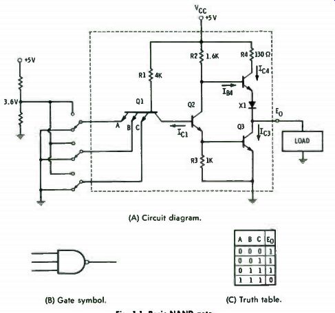
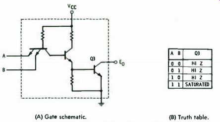
(A) Circuit diagram. (B) Gate symbol. (C) Truth table.
Fig. 1-1. Basic NAND gate.
The basic circuit of TTL is shown in Fig. 1-1. Except for the input transistor, the circuit is very straightforward. We will ignore the input transistor for the moment. Refer to the rest of the NAND gate, the output circuit, shown in Fig. 1-2. Let the base of transistor Q2 be grounded. With the base grounded, Q2 is a very high impedance, and hardly any current flows from the collector to the emitter. The voltage applied to the base of transistor Q3 is close to zero; thus, Q3 is also a very high impedance, or open. The collector of Q2, on the other hand, is close to 5 volts, and thus, transistor Q4 is strongly on -Q4 is saturated. The output voltage, E0, of the circuit is then a function of load current and the series impedance.
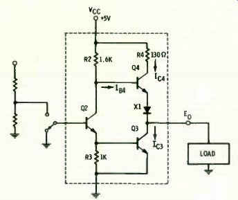
Fig. 1-2. Output circuit of Fig. 1-1.
The series impedance is the 130-ohm collector resistor of transistor Q4, the collector-to-emitter impedance of transistor Q4, and the forward impedance of the diode ( X1). The load is usually the inputs of other gates. With other gates as loads, the output voltage ( E0) will be approximately 3.5 volts-a logical 1 ( high). Turn the switch in Fig. 1-2 to point A so that about + 1.6 volts is applied to the base of transistor Q2. This is more than enough voltage to cause transistor Q2 to go into saturation.
With Q2 on, the voltage fed to the base of transistor Q3 rises, and Q3 is saturated. At the same time, the voltage at the collector of transistor Q2 drops from its previous value of close to 5 volts. This is the base drive to transistor Q4. For Q4 to conduct, its base must be about 1.8 volts. Impedances R2 and R3 have been selected so that when transistor Q2 is on, the base voltage to transistor Q3 is high enough to saturate Q3, and the base voltage to transistor Q4 is too low to turn Q4 on. Thus, transistor Q4 is cut off.
The output voltage of the circuit is now the saturation volt age of transistor Q3. Again, the load is the input circuits of the following gates. But the output voltage is near zero, and no current can flow out of the circuit through transistor Q4, since this transistor is off. What the output circuit can do, however, is to accept current from other sources, and this is how it is used. It is a current sink-a low impedance path to ground- for the input circuits of the succeeding gates.
The Input Circuit
Look at the input circuit of Fig. 1-1. We find an odd transistor with multiple emitters, and it is hooked up wrong.
How can transistor Q1 ever have any effect on transistor Q2? First, let all three emitters of Q1 be connected to ground through the toggle switches. The base of Q1 is connected to +5 volts through the 4K resistor; current flows through the base-to-emitter junctions; and transistor Q1 is strongly on- saturated. With transistor Q1 saturated, the voltage at its collector terminal is approximately the same as the voltage of its emitter terminal, which is at ground potential. Thus, the base of transistor Q2 is near ground potential, and the transistor is cut off. Any collector current that flows through Q1 to ground must go through a turned-off transistor ( Q2) . Current I ci is going to be very small. Since transistor Q2 is off, transistor Q4 is on; the output voltage is high, and the output of the gate is a high (a 1). Now, change the switch for emitter A of transistor Q1 and feed it a positive voltage. Let emitters B and C stay at ground potential or 0. What happens to transistor Q1? If any emitter of a multiemitter transistor is properly biased (in this case, connected to ground), the transistor acts like a normal single emitter transistor. Current from the base to emitter A ceases because the emitter voltage is higher than the base voltage; the base-to-emitter junction is reverse biased. Emitters B and C are still grounded, so they still conduct current. Transistor Q2 remains cut off.
Keep emitter A positive and connect emitter B to the positive voltage; leave emitter C grounded. What happens? Transistor Q1 is still turned on by emitter C; transistor Q2 is still cut off so the output stays high.
Now connect emitter C to the positive voltage so that all three inputs are high. No current flows to any emitter of transistor Q1 from the base of Q1. Thus, with all the emitters high, the base-to-collector junction of transistor Q1 becomes forward biased. There is current through the 4K resistor (R1) into the base of transistor Q2. Transistor Q2 is turned on, which causes transistor Q3 to turn on and transistor Q4 to cut off.
Connect any one of the three emitters of transistor Q1 to ground again. Immediately, Q1 goes into saturation, turning transistor Q2 off and driving the output to the high ( 1) state.
To summarize, the output will be a 1, if one or more inputs is a 0 ( or if all inputs are 0). Gate operation is summarized by the truth table shown in Fig. 1-1B. Output voltage Eo will be 0 only when all inputs are 1.
What if an input transistor has four or eight emitters, as some have? The same logic holds. If any one input is 0, the output is 1; only if all inputs are a 1 can the output be a 0. If we try to state the logical operation of the 3-input gate of Fig. 1-1, we have the statement: "When input A is a 1, AND input B is a 1, AND input C is a 1, the output is a 0." ( If we had been able to say that the output is a 1 when A AND B AND C are all is, we would have had an AND gate.) What we actually have is an AND gate plus a signal inversion-a Negated-AND gate or a NAND gate.
Totem Pole Output
Before going further, let us take a look at one of the peculiarities of TTL. Since the output of the gate is either a high or a low, either transistor Q3 or transistor Q4 must be on at all times. Because the schematic ( Fig. 1-1C) is drawn with transistor Q4 above transistor Q3, the output circuit looks like a totem pole although, in operation, the circuit acts much like a seesaw. We have assumed that when transistor Q3 turns on, transistor Q4 turns off simultaneously, and vice versa. In actuality, both output transistors are on at the same time during the transition. The result is that the output circuit shunts current to ground during the transition.
The "worst case" of current shunting occurs when the circuit is going from a 0 output to a 1 output. It takes transistor Q3 longer to turn off than it takes transistor Q4 to turn on.
The result is a spike of excess current, as shown in Fig. 1-3.
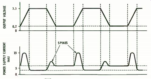
Fig. 1-3. Gate current spikes during changes of gate output.
When the output goes from 1 to 0, excess current is again drawn, but not as much because transistor Q4 is driven into the off state quickly, rather than being allowed to decrease to it naturally ( as transistor Q3 does during the transition from 0 to 1) . One result of current spiking is that the system's power consumption increases with the speed of circuit operation- that is, with the clock rate of the system. For type 54/74 logic, the quiescent (clock stopped, nothing happening) dissipation is about 6 mW per gate. With the clock running at
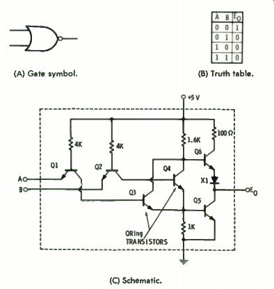
(A) Gate symbol. (C) Schematic.
Fig. 1-4. Basic NOR gate. (B) Truth table.
, 10 MHz, the dissipation is about 10 mW per gate; at 20 MHz, it is about 20 mW per gate. Thus the change in power consumption, as a function of operating frequency, is substantial. however, since the clock rate in a given system is usually fixed, changes in power supply requirements do not normally occur when the system is operated with the clock off. But, if many gates in a system all have to change simultaneously, a large amount of current may be demanded, with resultant spill-over effects on voltage regulation and transient (noise) characteristics.
NOR GATES
While a logic family is built around one gate, you still have to perform other functions. The two basic functions in all types of digital logic are AND, and OR; except that in TTL, these become NAND and NOR. The development of a NOR gate from the basic NAND gate is straightforward. The circuit is shown in Fig. 1-4. If both input A and input B are high, then transistors Q3 and Q4 are on.
Transistor Q5 is also on; thus, the output of the gate is 0. If input A goes low while input B remains high, transistor Q3 turns off, but Q4 stays on and holds Q5 on; the output is 0. Similarly, if input B goes low while input A remains high, the output is still 0. Thus, the output is 0 if either input A OR input B is a 1, and the function is a Negated-OR or NOR. If both A and B are 0, then both transistor Q3 and transistor Q4 are off; Q5 is cut off, and transistor Q6 is turned on. The output is a 1. The truth table ( Fig. 1-4B) shows the various conditions of the circuit.
INVERTERS
A recurring problem in digital systems is a signal that appears as a high instead of a low, or as a low instead of a high.
The problem is easily solved by using an inverter to change a 0 to a 1, or a 1 to a 0. The symbol ( s) and truth table for an inverter is shown in Fig. 1-5.
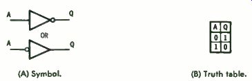
(A) Symbol ( B) Truth table.
Fig. 1-5. Inverter function.
A simple inverter can be made from a single transistor as shown in Fig. 1-6. When input A is high, the transistor is saturated, and the output voltage E0 is low. When input A is 0 or low, the transistor is essentially an open circuit, and E0 is high ( 1). The single-transistor inverter is sometimes used in the output circuits of complex ICs to provide buffering and/or inversion. The circuit type 5404/7404, called a Hex Inverter, is more complex. It consists of six identical TTL inverter gates with common \T ee and ground connections. The circuit ( Fig. 1-7), a 1-input NAND gate, is the schematic of each inverter in the IC. When an inverter is needed but is not readily available, the two inputs of a NAND gate can be permanently connected together. ( Also, one input of a NAND gate can be permanently connected to a 1.) It will then function as a simple inverter. A NOR gate can also function as an inverter if one input is connected permanently to ground.
In more complex ICs, inversion may be obtained by any one of the above methods. Regardless of the method used, the inverter symbol ( s) shown in Fig. 1-5 is used on the logic diagrams.
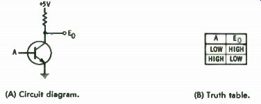
(A) Circuit diagram. (B) Truth table.
Fig. 1-6. Simple transistor inverter.
AND-OR-INVERT GATES
One step beyond the NOR gate is the AND-OR-INVERT gate.
The circuit, truth table, and symbol are shown in Fig. 1-8. The output is 0 if both A and B are is or if C and D are is. The circuit is the equivalent of a NOR gate with multiemitter ANDing transistors.
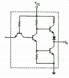
Fig. 1-7. One-input NAND gate inverter.
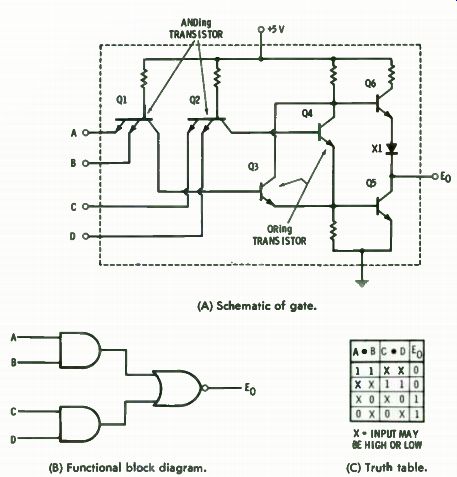
(A) Schematic of gate.
(B) Functional block diagram. (C) Truth table.
Fig. 1-8. An AND-OR-Invert gate.
The function is thus an AND-OR with an inverted output.
Naming a function of this kind is tricky. If the convention used with the NAND and NOR gates was followed, you would say you have a negated AND-OR gate, which you might call a NANDOR. But this convention was not followed, and the people who name logic designs used the more precise AND-OR-INVERT.
OPEN-COLLECTOR AND WIRED- OR CIRCUITS
A major disadvantage of the totem pole output is that it prevents the use of the so-called wired-OR circuit that has been widely used in other logic families, particularly in diode-transistor-logic ( DTL) . When two TTL outputs are tied together, and if one gate has a high output and the other has a low output, the high gate will drive an excessive amount of current into the low gate. Obviously, this is not good.
The lack of the wired-OR connection requires that the output of the basic TTL gate be buffered when the logic so demands.
This means extra circuits. To get around this, manufacturers have developed modified circuits, wherein transistor Q4 in the output circuit is omitted and the collector of transistor Q3 is left open, as shown in Fig. 1-9.
The truth table shows that the circuit functions as a NAND gate, except that transistor Q3 operates much like a toggle switch. When the A and B inputs are high, transistor Q3 is saturated and its series impedance from collector to emitter is very low. When either A or B input is low, transistor Q3 has no base drive and is a very high impedance. A load, such as a Vcc Q3 AB Q3
(A) Gate schematic. ( B) Truth table
Fig. 1-9. Open-collector, 2-input NAND gate.
lamp or relay, can be driven by a separate voltage source greater than the normal 5-volts source, as long as the current rating and breakdown voltage of transistor Q3 is not exceeded.
In certain IC circuits designed to drive cold-cathode glow tubes, transistors having a high breakdown voltage are provided.
The wired- os circuit is shown in Fig. 1-10. As long as all three output transistors are off ( high Z) , the common tie point has a high impedance to ground. If any one of the three transistors is saturated, the common point is brought close to ground.
The wired-OR circuit can also be interpreted as a wired-AND. Output impedance will be high only if A is high, AND B is high, AND C is high. Otherwise, the output impedance is low.
When the voltage present at the common tie point is used as an input to a gate, a so-called " pull-up" resistor may be necessary ( as shown in Fig. 1-11). When all the transistors are cut off, the pull-up resistor provides a source of positive volt age to the load.
(A) Circuit diagram.
Fig. 1-10. A wired-OR circuit.
(B) Symbol.
EXPANDABLE GATES
In logic circuits, many inputs of the AND-OR type often need to be handled. To meet these needs, integrated circuits having many inputs have been developed. Further, some of these ICs bring certain tie points outside the IC package to allow the logic to be expanded and thus handle more complex jobs. This operation can best be understood by an example.
A typical expandable gate, circuit type 5450/7450, is shown in Fig. 1-12. The device is called an " Expandable Dual 2-Wide,
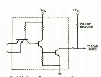
Fig. 1-11. Open-collector gate with pull-up resistor.
2-Input AND-OR-INVERT gate." We have already discussed the AND-OR-INVERT part of the description. The "2-Input" means that each AND gate has two inputs. ( Some gates have 3-inputs, some 4, some 8, etc.) The "2-Wide" means that each part of the OR gate is fed by an AND gate. ( Thus, two AND gates feed one OR gate). The function of the device is much clearer when shown by logic symbols as in Fig. 1-13. The "Dual" means that the IC contains two complete circuits. The word "Dual" is being used somewhat loosely by the manufacturers as the type 5450/7450 IC package does contain two separate 2-wide 2-in put AND-OR-INVERT gate circuits, but only one of the gates is expandable. The other is a plain gate.
The only word left in the description is "Expandable," and this turns out to be straightforward. In the development of
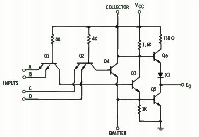
Fig. 1-12. An expandable 2- wide 2- input AND-OR- Invert gate.
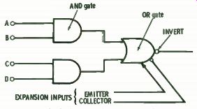
Fig. 1-13. Block diagram for an expandable gate.
the NOR-gate function, we saw how transistors Q3 and Q4 were utilized to form an °Ring function. In Fig. 1-12, we see that the common points (the collectors and emitters) of ORing transistors Q3 and Q4 have been brought outside the IC to allow external connections.
The circuit shown in Fig. 1-14A is for a type 54/7460 Dual 4-Input Expander. The logic diagram for the expander is shown in Fig. 1-14B. All you have to do is connect input transistor Q1 to a -45-volts supply voltage and then connect the ORing transistor outputs to the equivalent points of a type 5450 or 7450 expandable gate. Thus, you have expanded the logic function to perform as indicated in Fig. 1-15. That is, you now have 3 AND gates ( two with 2 inputs and one with 4 inputs) feeding an OR gate; the 0R-gate output is then inverted.
What if you wanted to hang two expanders onto the expand able section of a type 5450 or 7450 circuit? Could you do it? A close look at the basic circuits shows that the input circuits are not affected and neither are the output transistors.
Furthermore, if one of the °Ring transistors is saturated, then the effect of turning on another °Ring transistor will be negligible. But connecting expanders adds capacitance to the circuit ( at point A in Fig. 1-12), which slows things down.

(A) Schematic. (B) Block diagram.
Fig. 1-14. Four-input expander.
Expansion is thus usually limited to 4 or 5 expanders. ( A total of four expander gates may be connected to the expander inputs of a type 5450 or 7450 gate.)
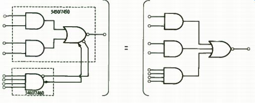
Fig. 1-15. Diagram for expandable gate with expander.
LOADING RULES
Most digital circuits talk to other digital circuits. Only rarely must a gate talk to the outside world, such as operating an indicator light or working into an interface circuit of some kind. Because so much digital conversation is gate to gate, the input and output circuits have been matched as far as possible to make things simple and easy.
The circuit shown in Fig. 1-16 illustrates the loading situation. Gate 1 is high and delivering current, and Gate B is low and is sinking current. Gate 3 has 3 inputs, one of which is permanently connected to a source of +3.5 volts. Input B can be manually connected to either +3.5 volts or to ground. Input C is driven by Gate 1. Since all three inputs of Gate 3 are high, the output of the gate will be low. The toggle switch option on input B allows this input to be driven low when desired, which will drive the gate high. This function is useful if registers, flip-flops, or memories are to be manually loaded.
The current flow into the emitters of Gate 3 is the reverse leakage current of the diode junctions. Since each emitter forms a diode, each draws leakage current, typically about 40 A. Input A of Gate 4 is permanently connected to +5 volts through a 1K resistor. This keeps input A high, yet protects it if the supply voltage should rise above its normal maximum level of 5.5 volts. Inputs B and C of Gate 4 are driven by Gate 1, and each draws about 40 A. Gate 4 is satisfied and its output is low.
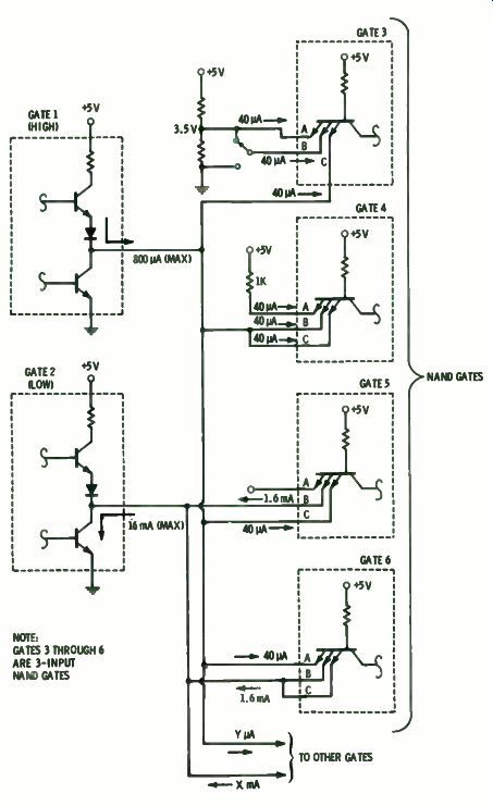
Fig. 1-16. Gate-to-gate loading conditions.
Input A of Gate 5 is open. As a result, no current flows in or out of the emitter, and the input acts as if it were permanently high. When an input is left open, it is subject to noise pickup. Further, the distributed capacitance of the open input slows down the operation of the gate. Thus, open inputs are undesirable. Input B is connected to ground through Gate 2.
Approximately 1.6 mA will flow from Gate 5 to Gate 2; Gate 5 is driven high. The 40 uA into input C of Gate 5 is swallowed up by the 1.6 mA out of the same transistor. ( The ratio: 1.6 mA/40 A = 40.) Gate 6 has 40 µA input into emitter A and 1.6 mA out of emitters B and C combined. ( Once any emitter is driven low, the input transistor is driven into saturation and thus cannot supply significantly more current even when other emitters go low.) Thus if Gate 1 should also go low, the 1.6 mA out of Gate 6 would be split up, with 1 / 3 going to Gate 1 and % to Gate 2.
For ease in circuit design, the 40 µA into an emitter is de fined as a unit load for a high gate ( Gate 1), and the 1.6 mA out of an input transistor is defined as a unit load for a low gate ( Gate 2). The maximum current that can be sunk into a low gate without causing the output voltage to rise above the maximum limit of 0.4 volt is 16 mA. As a result, a low gate can drive 10 inputs; the fan-out is ten.
The maximum current that a high gate can deliver is 800 µA. Thus, the fan-out for a high gate is 800 µA/40 = 20 unit loads.
The allowable fan-out, therefore, is 10 when a gate is low and 20 when it is high. The lower fan-out must be observed as long as the gate is allowed to go both low and high. When a gate is going to be permanently high, the higher fan-out can be used.
NOISE IMMUNITY
All electronic circuits have trouble with noise and, although digital circuits are far more resistant to noise than analog circuits, they are not immune. If a large motor starts up near the digital circuit, or a bulldozer is driven through a buried cable connected to the circuitry just as a flip-flop is about to flop, it is possible that the flip-flop will not flop but will stay in the flip state. The resulting error may or may not be serious. If the digital information is being stored in a computer memory, the error may never be found.
Digital designers tend to get edgy if errors occur more than about once in 10 million bits of data. System designers do not like flip-flops that flop when they shouldn't or don't flop when they should. Gates that open when they should close, or vice versa, irritate them. Not much can be done to stop roving, errant bulldozers, but errors from other sources tend to be more manageable. Error prevention is based primarily on the naturally high noise immunity of digital circuits.
The input/output characteristics of the basic TTL gate, shown in Fig. 1-17, indicates how noise immunity is achieved.
Let input A of the NAND gate be high, and let input B be driven by voltage E1 . Output voltage is then controlled by Ein. When Eh, is 0, E0 will be high and will normally be somewhere between +2.4 and +3.9 volts ( Region I of Fig. 1-18). The actual value of E0 is determined by a number of variables. If the gate is operating in a high ambient temperature, then E0 will be on the high side. If the ambient temperature is down around -55° C, Eo will be low.
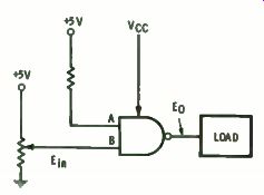
Fig. 1-17. Input/output characteristics of TTL gate.
Another factor affecting E0 is the load, which means the fan-out on the gate. The voltage of the power supply feeding the gate obviously affects Eo. Military versions of TTL allow Vœ to be anywhere between 4.5 and 5.5 volts. Commercial versions normally require Voc to be between 4.75 and 5.25 volts. When E0 is in the high state, it tracks Voe fairly closely.
When E0 is in the low state, it is not affected much by Vœ . Still another variable is the individual gate itself. Although quality control in the manufacture of ICs is extremely high, differences in materials, mask alignments, dopant purity, furnace temperatures, processing time, etc., cause minute changes from one circuit to the next. One result is minor changes in Eo.
What happens to the output voltage, Eo, as the input volt age, El ., is slowly increased from 0 to maximum? Assuming that E0 is tracking along the low limit line in Fig. 1-18, it will be 2.4 volts at El . = 0. Then E0 will start to decrease when Ein changes to 0.75 volt. As El increases from about 0.80 to 1.1 volts, E0 falls rapidly to about 0.2 volt, the saturation voltage of the output transistor. Now, start again with El . at 0 volt and assume E0 tracks along the high limit line. Output voltage E0 is more sensitive to the input voltage ( E1 .), but it does not drop below 2.4 volts until Ein is about 1.0 volt. When El . reaches 1.4 volts, E0 is minimum and will be less than 0.4 volt.
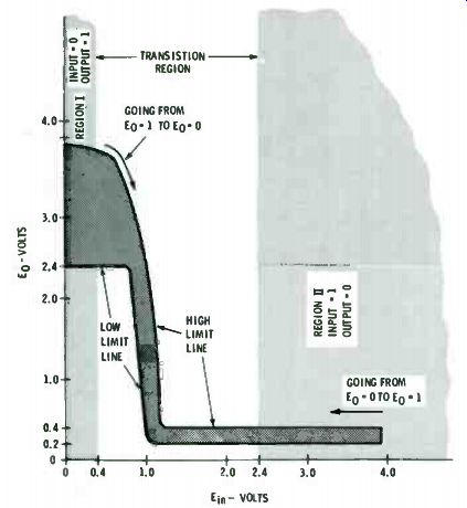
Fig. 1-18. Noise margin.
When a gate is low, its maximum output is 0.4 volt. This is 0.7 volt below the minimum of 1.1 volts needed to cause the next gate to act as if it sees a high. This 0.7 volt is the noise margin. It protects the driven gate from seeing a false 1 ( generated by noise spikes on the signal line) . Similar considerations apply when we want to drive a gate high. In this case, the input voltage El starts out in Region II (Fig. 1-18) and tracks along either the high or the low limit line. In one example, E0 begins to go high when Ein falls to 1.3 volts, and in the other example, when El0 falls to about 1.1 volts. In either case, E0 is always above 2.4 volts whenever Ein is below 0.75 volt. Since the maximum output from a low driving gate is 0.4 volt, the "worst case" noise margin protecting a driven gate from seeing a false 0 (generated by noise) is:
0.75 - 0.4 = 0.35 volt.
In most systems, the noise margins will be better than the values just noted. For operation at typical ambient temperatures around 25° C ( about 68° F), the noise margin for TTL systems is generally stated by manufacturers to be about 1.2 volts.
So far we have considered noise as occurring only on the input or signal line. Noise can also occur on both the power supply line and the ground wires. Any spikes or transients, up to about 3 volts, occurring on the power supply line will usually not cause false gate operation; neither will any spikes of about 1 volt occurring on the ground line. Further, the spike must last for a period of about 50 nanoseconds before it causes any trouble. ( Spikes occurring on the signal line only have to last for a period of about 20 nanoseconds before they start causing errors.) As noted earlier, TTL is a fast logic, and the gates will change from Region I to Region II ( Fig. 1-18) in about 10 ns.
When you try to turn gates on and off in that short a time, you are dealing with outputs that are changing at the rate of 1.6 million amps per second ( 1.6 mA/10 ns) and 2.5 billion volts per second (2.5 V/10 ns). All the noise protection you can possibly get is needed. One of the secrets to obtaining a noise-free TTL system is to have as much bypass capacitance in the Vce line as possible. Also, use a decent size wire in the Vec line- size No. 20 wire or larger is recommended.
Next: FLIP-FLOPS
Guide Index : Transistor-Transistor Logic (early 1970s)