Flip-flops form a class of basic circuits vital in all forms of digital logic. Flip-flops can store digital data, remember in formation, and they can count. A number of basic types have been developed and they are used in a great variety of ways.
A flip-flop can be formed from just two cross-coupled transistors ( method used in memory circuits where simplicity is desired), but most TTL flip-flops are made from NAND or NOR gates. Fig. 2-1 shows two NAND gates connected to operate as a single flip-flop. ( Vcc and ground connections are not shown on logic diagrams. However, when a circuit is constructed, all the power supplies, grounds, floating inputs, circuit loads, etc., must be considered.)
SET-RESET FLIP-FLOPS
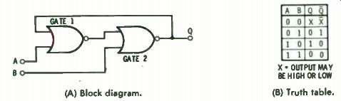
The flip-flop in Fig. 2-1 has two inputs ( A and B) and one output ( Q). Each input can be a 1 or a 0, and Q can be either 1 or 0. Four combinations of inputs are possible, excluding inputs left open which is the equivalent of being high or 1.
Fig. 2-2 shows logic diagrams for the four possibilities, where: (1) A = 0, B = 0; ( 2) A = 0, B = 1; (3) A = 1, B = 0; and A = 1, B = 1. What will the output ( Q) be for each set of inputs ?
First, consider A = 1 and B = 0, as shown in Fig. 2-2A. Note from the truth table ( Fig. 2-1) that for a 2-input NAND gate, if either input is 0, the output of the gate must be 1. On the other hand, if only one input to a NAND gate is known and it
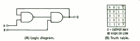
(A) Logic diagram ( B) Truth table.
Fig. 2-1. A NAND-gate Set-Reset flip-flop.
is a 1, then the output of the gate is not known. The output can be 0 or 1, depending on the other input.
We see that with inputs as shown in Fig. 2-2A, Gate 2 is driven to an output of Q = 1, because input B is 0. This in turn causes Gate 1 to have a 1 for both inputs, and thus to have an output of 0, as required by the truth table for NAND gates.
(Gate 1 output of 0 is the second input for Gate 2. Two low inputs to NAND Gate 2 make Q = 1). Suppose the inputs are suddenly changed so that A = 0 and B = 1, as shown in Fig. 2-2B; what happens? Gate 1, with at least one of its inputs 0, must have a 1 out. This means both inputs of Gate 2 are a 1, and its output is 0. If we call the state of the gates in Fig. 2-2A the flip state, then Fig. 2-2B is the flop state.
Two other sets of inputs are possible. A = B = 0 and A = B = 1.
Fig. 2-2C shows the state of the circuit when A = B = 0. Both gates are driven to 1 and the output is a 1. In Figs. 2-2A and 2-2C, B = 0 and controls the output; in Fig. 2-2B, A alone is 0 and is in control. In Fig. 2-2D, A = B = 1 and neither is in control. Thus, the output of the circuit in Fig. 2-2D can be 0 or 1.
The circuit of Fig. 2-2D can be considered the quiescent state of the flip-flop. The flip-flop is set to one state or the Q.1 Q 1 A-0
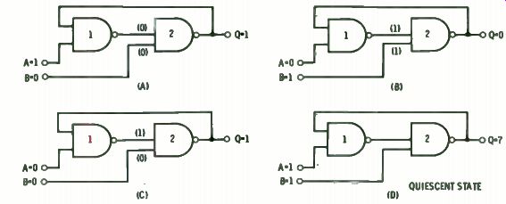
Fig. 2-2. Different input/output conditions for Fig. 2-1A.
... other by setting one input to 0 while the other is high. If both inputs are then brought high, the flip-flop will remain as set.
One further state of operation needs to be considered. Sup pose all power to the circuit has been off and is suddenly turned on. What state does the flip-flop take when the circuit stabilizes? Only the condition shown by Fig. 2-2D is uncertain and, in this case, the output can be either 1 or 0.
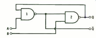
Fig.
2-3. Negative output- Is.
From the above considerations, the truth table of Fig. 2-1B is constructed. Note that the truth table contains a heading for Q, and that Q is the negative of Q. ( A negative of the output Q always exists in a flip-flop, as shown in Fig. 2-3. The Q output, however, is not always accessible for use.) The un known "X" in the truth table indicates that the status of the output is not predictable. The symbol X is used to show that Q will be the opposite of the output Q.
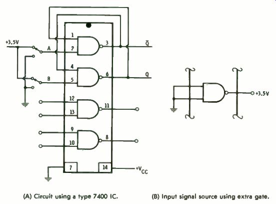
(A) Circuit using a type 7400 IC. (B) Input signal source using extra gate.
Fig. 2-4. Constructing a Set-Reset flip-flop.
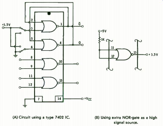
The above flip-flop is known as a Set-Reset type since it can be set to one condition and reset to the other at any time, in accordance with the truth table. A Set-Reset flip-flop can be constructed using one type 7400 IC, as shown in Fig. 2-4.
Since the 7400 device contains four NAND gates, you can actually build two complete and independent flip-flops. The simplicity of connecting such building blocks together is one of the major advantages of digital circuits.
(A) Block diagram. (B) Truth table.
Fig. 2-5. A NOR-gate flip-flop.
The circuit shown in Fig. 2-4A includes both Q and ( 1 outputs. It uses toggle switches to set the inputs to 1 or 0. A convenient source of input signal is to use one of the unused NAND gates, connected as shown in Fig. 2-4B.
NOR-GATE FLIP-FLOPS
Flip-flops can also be built with NOR gates, as shown in Fig. 2-5. Although the circuit is very similar to the NAND gate flip flop of Fig. 2-1, it does have a few subtle differences. The truth table for a NOR gate shows that a 1 input is controlling and always drives the gate to 0. From this reasoning, the states indicated in Fig. 2-6 are obtained.
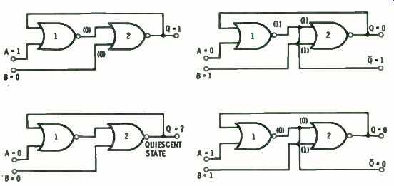
Fig. 2 - 6. Different input/output conditions for Fig. 2 - 5A.
(A) Symbol.
In the NoR-gate flip-flop, the input conditions of A = B = 1 give Q = Q = 0. The NAND-gate inputs of A = B = 0 gave Q = Q = 1. An uncertain output is obtained with a NOR-gate flip flop when A = B = 0, and in a NAND-gate flip-flop when A = B = 1.
In building logic circuits, the designer does not want to be required to declare that a particular flip-flop must be a NAND-gate type, while an identical nearby flip-flop is to be a NOR-gate type. Two of the four possible sets of inputs for both NAND- and NOR-gate flip-flops do give unambiguous results, however. As long as the logic designer ensures that only these two sets of inputs are applied to the inputs, he can use NAND gate and NOR-gate flip-flops interchangeably. ( The two sets of inputs that give unambiguous results with both types are A = 1 with B = 0, and A = 0 with B = 1.) The labeling of the inputs and the Q and « Q outputs is entirely arbitrary. Therefore, instead of calling the inputs A and B, we can call one the Set input ( S) and the other the Reset input (R). This leads to the Set-Reset flip-flop symbol shown in Fig. 2-7 and its truth table. The Q and Q outputs are labeled to agree with the truth table.
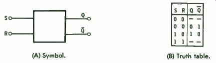
(B) Truth table.
Fig. 2-7. A Sof-Reset flip-flop.
A NOR-gate flip-flop can be constructed with a circuit type 7402, as shown in Fig. 2-8A. As with the quadruple NAND device, one of the unused gates can serve as a source of 3.5 volts, a 1 ( Fig. 2-8B).
CLOCKED FLIP FLOPS
While the Set-Reset flip-flop has many uses, it has one characteristic that is a disadvantage in many logic schemes. When ever the inputs to a Set-Reset flip-flop change, the output changes immediately. It is delayed only by the charge storage characteristics of the semiconductor devices used to make the gates. The delay is only a few nanoseconds and is unpredictable so far as a specific device is concerned.
Assume that the inputs to the flip-flop are measurements being made by the navigation system of an aircraft, and the output of the flip-flop will aid in the control of the autopilot.
If the input data changes rapidly, operation of the controls might be erratic, leading to excessive wear of parts and un reliable control. To prevent wild changes in operation, digital systems usually work on a controlled stop-and-go basis. The system is paced by a clock, which is actually an oscillator.
(A) Circuit using a type 7402 IC. (B) Using extra NOR-gate as a high signal source.
Fig. 2-8. Constructing a NOR-gate flip-flop.
The clock usually acts as a pacing signal, allowing the system to rest most of the time. Then, when all the various sub systems have settled down to a stable condition, it scans all the inputs and outputs to see if something should be changed.
In a digital computer, on the other hand, the clock moves the program to the next instruction once the circuits have settled.
In a computer, the tendency is to operate at as high a clock rate as possible, so that longer and more complex programs can be handled with as little electronics as possible. In a control system, the clock need only be fast enough to stay ahead of the process or machine being controlled.
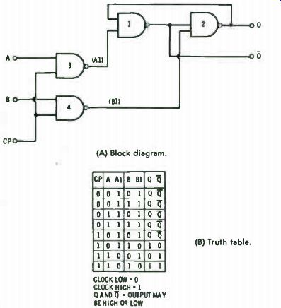
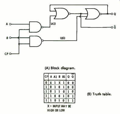
The clock signal in a digital system is a square wave of volt age having the same magnitude as the logic signals. The signal must meet certain requirements on rise time, fall time, and duration of being high and low. Many digital circuits are activated when the clock goes high-that is, goes to 1. Some circuits are activated when the clock goes to 0. Fig. 2-9 shows how an S-R flip-flop can operate in a clocked system. The circuit shows a NAND-gate S-R flip-flop consisting of Gates 1 and 2. Inputs to the flip-flop are Al and Bl. Input Al is the output of Gate 3, which is a function of input A and the clock pulse CP. When A is 1 and the clock is 1, then Al is low. Similar action controls input B and Gate 4 output, B1.
When the clock is low, both Al and B1 will be high.
The truth table shows how the flip-flop is controlled. As long as the clock pulse signal is 0, Al and B1 will both be 1 and the flip-flop will not change state. However, as soon as CP goes high, input signals A and B control the flip-flop. Thus, if A = 1 and B = 0: Al is 0, B1 is 1, Q goes to 0, and Q goes to 1. If A = 0 and B = 1, Q goes to 1.
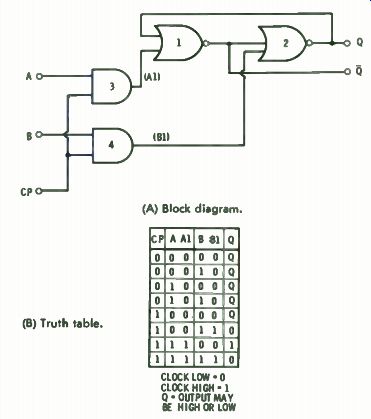
The circuit of Fig. 2-10 shows a NOR-gate flip-flop with AND-gate control. The truth tables in Figs. 2-9 and 2-10 are similar, except that the outputs are different for A = B = 1 when CP is 1. We see also that in the NAND-gate circuit, when ...
(A) Block diagram. (B) Truth table.
Fig. 2- 9. Clocked NAND-gate S- R flip-flop.
A = 0 and B = 1, Q goes to 1; while in the NOR-gate circuit, the same inputs give Q = 0. A NAND-gate flip-flop controlled by AND gates is shown in Fig. 2-11. Whenever CP goes to 0, Al and B1 go to 0, and Q and Q go to a 1. The circuit does not function correctly. Fig. 2-12 shows a NOR-gate flip-flop with NAND-gate control; this circuit does not work correctly either, since Q and Q go to 0 when CP goes to 0.
(A) Block diagram.
(B) Truth table.
Fig. 2-10. Clocked NOR-gate S- R flip-flop.
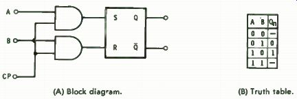
Fig. 2-13 shows the equivalent logic circuit of Fig. 2-10.
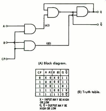
The truth table has been reduced to show only the inputs that are significant. The output column is labeled Q.. This refers to the state that the clock pulse and the inputs have caused the flip-flop to enter. Excluded inputs are A = B = 0 and A = B = 1. As long as the CP = 0, the inputs will have no effect on the flip-flop. When CP goes high, the flip-flop will take up the state called for.
If A and B should change while CP is high, the flip-flop will follow accordingly. Thus, the inputs are usually required to be stable while the clock is high and data is being entered into the flip-flop. Stability requirements are not difficult to meet
(A) Block diagram. (B) Truth table.
Fig. 2-11. NAND-gate flip-flop controlled by AND gate.
(A) Block diagram. (B) Truth table.
Fig. 2-12. NOR-gate flip-flop controlled by NAND gate.
... but must not be ignored. When CP goes low, the flip-flop goes to its quiescent state.
A clocked flip-flop can be easily constructed using a 7400 and ...
(A) Block diagram (B) Truth table.
Fig. 2-13. A clocked S- R flip-flop.
TTL FLIP-FLOPS
In working with digital logic, circuit designers found that certain types of flip-flops were particularly useful. As a result, semiconductor manufacturers started making ICs containing these flip-flops; sometimes one flip-flop to an IC pack age, sometimes two.
The general-purpose flip-flops available in the type 54/74 family are the D type, the J-K type, and the J-K Master-Slave type. Simpler Set-Reset and clocked Set-Reset flip-flops are used internally in other ICs, such as shift registers and counters, and have recently become available in ICs. Other TTL families do have other types of flip-flops.
D-Type Flip-Flop
The D-type flip-flop is a clocked flip-flop with a very simple truth table. The device has only one input, which is labeled D for Data and which may be either 1 or 0. When the clock pulse occurs, the output of the flip-flop goes to the same state as the D input.
Fig. 2-14 shows the logic diagram of a D-type flip-flop. Two flip-flops are included in the circuit type 5474 or 7474 package.
It is called a "Dual D-Type Edge-Triggered Flip-Flop." The circuit has four input terminals: Preset, Clear, Clock, and D. The outputs are Q and Q. As usual, ground and power connections are not shown on the logic diagram. The flip-flop is shown in the functional block diagram form in Fig. 2-14A and is shown in simplified block form in Fig. 2-14B. Operation of the circuit will be examined using the analysis table in Fig. 2-15.
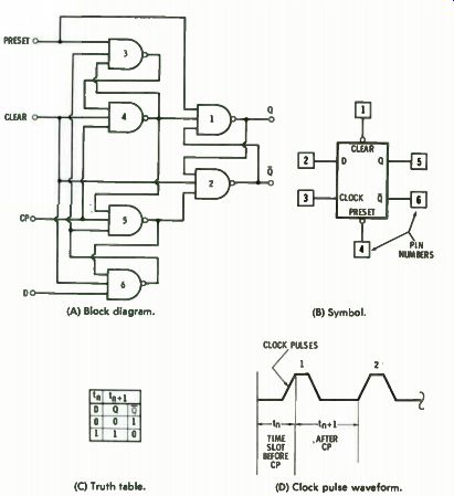
(A) Block diagram. (B) Symbol. (C) Truth table. (D) Clock pulse waveform.
Fig. 2-14. A D-type flip-flop.
The catalog description of the D-type flip-flop states that a low input to the Preset ( P) terminal sets output Q to a logical 1, and a low input to Clear ( C) terminal sets Q to a logical 0. (The gates have been labeled 1 through 6 to aid the discussion.)
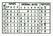
Fig. 2-15. Analysis table for Fig. 2-14.
Since the inputs must control the final state of the circuit, we can check circuit operation by varying the inputs one at a time. We are interested in the final condition of Gates 1 and 2, since these provide the outputs Q and Q. Try to follow both the logic diagram in Fig. 2-14 and the analysis table in Fig. 2-15. We see that when CP = 0, the outputs of Gates 4 and 5 go to a logical 1, and D = 0 causes Gate 6 to go to a 1. Thus, Gate 3 has all its inputs as 1; its output is 0. Since Gate 4 is already 1, the fact that the output of Gate 3 is 0 does not change anything. We see that Gates 1 and 2 have not been affected by the other gates and, thus, their status is unknown. The outputs of Gates 1 and 2 are Q and Q and are stable; whichever output happens to become a 0 will drive the other output to a 1.
The second line of the analysis table shows what happens when the P input goes to 0, with other inputs unchanged. Gates 1 and 3 go to 1, so Q = 1. The Clock is 0 and holds Gate 4 and Gate 5 high, while D = 0 holds Gate 6 at a 1. The input to Gate 2 is a 1 from C, a 1 from Gate 5, and Q = 1; thus, the output of Gate 2 is 0. The flip-flop has been set to Q = 1, Q = 0. Suppose the Clock or D (or both) should become 1 while P is low-will this affect the circuit? We note that as long as P = 0, Q must be 1. From line 7 of the analysis table, we see that Gate 5 will be 1 because Gate 4 or Gate 6 will be 0 if CP or D are high; therefore, Gate 2 is a 0. Thus, when P = 0, it overrides CP and D, regardless of whether they are 1 or 0. The third line of the truth table shows how the Clear input resets the circuit. With C = 0 and P = 1, Gate 4 is a 1 and Gate 2 is a 1; Gate 1 has all is as inputs and therefore is a 0. Again, the CP and D inputs cannot affect the outputs. If, however, both P and C were 0, the outputs would be driven to a 1 ( Q = 1 and Q = 1). This is a forbidden or illogical state of affairs, and so this combination of inputs is forbidden.
In normal use, the flip-flop operates with P = C = 1, and data ( D) is entered into the flip-flop as the clock goes high.
Line 4 of the analysis table shows what occurs when CP = 1 and D = 0. We see that prior to CP = 1 (that is, line 1) , Gate 4 was 1 and Gate 3 was 0. When CP goes to 1, Gate 5 has all 1 inputs (output from Gates 6 and 4 and CP), thus its output goes to 0; this is similar for Gate 3, which also goes to 0. Therefore, Gate 5 = 0 makes Gate 2 = Q = 1, while Gate 1 has all is as inputs ( P, Gate 4 and f 7 .1), so Gate 1 = Q = 0. Thus, the Clock has transferred the D = 0 input to the Q = 0 output.
When the Clock falls back to zero, line 1 of the truth table applies, and the flip-flop is quiescent at Q = 0 and CI = 1.
When D = 1, the flip-flop goes to Q = 1 when CP = 1. Prior to the CP going to 1, but with D = 1, the circuit is as shown in line 5. Because CP = 0, Gates 4 and 5 are high; therefore, Gate 6 has all is as inputs and is 0; therefore, Gate 3 has all is as inputs and is 0. Gate 1 inputs are P = 1, Gate 4 = 1, and Q; while Gate 2 inputs are C = 1, Gate 5 = 1 and Q. Thus, Gates 1 and 2 are quiescent.
When CP goes to 1 ( line 6), Gate 4 goes to 0, which gives Gate 5 a 1 output. Gate 3 is a 1, Gate 1 is a 1, and Gates 6 and 2 have all 1 inputs and therefore go to 0. Thus Q = 1 and Q = 0. When CP falls back to 0, the circuit returns to line 1 or line 5.
Because of the way the circuit operates, it is called edge triggered, and the data on D is transferred to the flip-flop on the positive-going edge of the clock pulse. Once the circuit has responded to CP, the D input is locked out and a change here has no effect until the next clock pulse.
The truth table for a D-type flip-flop is shown in Fig. 2-14C. Only one input, D, is listed and only one output is needed, although both Q and Q are shown. The symbol t, refers to the time slot ( Fig. 2-14D) before the clock pulse. The symbol t. + 1 means the time slot after the clock pulse. The interpretation, therefore, is that if D = 0 before the clock pulse, Q will be 0 after the pulse; if D = 1 before, Q will be 1 afterwards.
The block symbol ( Fig. 2-14B) for the complete flip-flop shows open circles on the Clear and Preset inputs. These open circles mean that when the Clear input is driven to 0, it clears the flip-flop ( sets Q to 0); when P = 0, the flip-flop is preset to Q = 1. In some cases, a diagram will show an input with a line above it, such as C. This means that U = 0 is the signal that causes action. In some cases, the line drawn above an input is used together with an open circle on the diagram. This is redundancy or emphasis only, and the line does not negate the open circle, nor does the open circle negate the line.
Note further that the open circle is placed in direct contact with the block diagram outline. When an open circle is drawn some distance away from a block, it usually is meant to show a pin on the IC package; it is not, in this case, a negation symbol.
J-K Master-Slave Flip-Flop
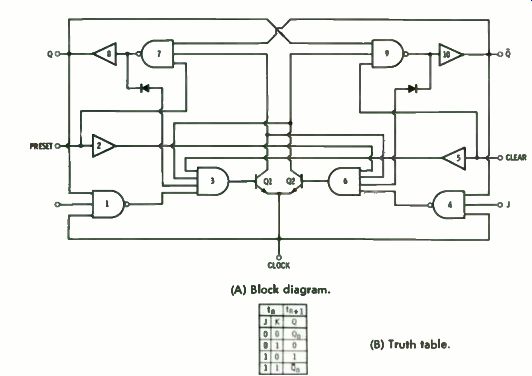
The most popular flip-flop is the so-called J-K flip-flop. The letters J and K have no special meaning and may, in fact, have been merely the label put on the pins (used for inputs) when the circuit was developed. The functional block diagram of a J-K Master-Slave flip-flop type 5473/7473 is shown in Fig. 2-16. Gates 3 and 6 form the master flip-flop, and Gates 9 and 10 form the slave.
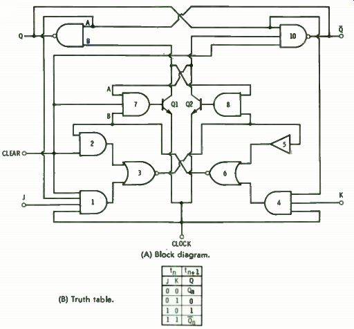
(A) Block diagram. (B) Truth table
Fig. 2-16..1-K Master-Slave flip-flop.
The truth table for the circuit shows four types of operation.
When inputs J and K are 0, the flip-flop is in the quiescent state and does nothing as clock signals come in. This is shown in the truth table by the notation Q., which means that the output Q is the same, in time slot t t , + 1 , as it was in time slot t,, When J = 0 and K = 1, the clock drives the output Q to 0; when J = 1 and K = 0, Q is driven to a 1. Finally, when J and K are both 1, the clock signal causes the flip-flop to change state, or toggle, regardless of whether the previous state was 0 or 1.
Thus all four possible inputs are allowed, and each produces its own specific result.
The flip-flop is cleared ( Q = 0) as indicated in line 1 of the analysis table ( Fig. 2-17). The X notation for inputs J, K, and Clock means that the circuit doesn't care whether these inputs are 1 or 0-they do not affect the output. A low (0) on the Clear input causes Gate 10 to go to high ( 1). Gate 7 output is ...
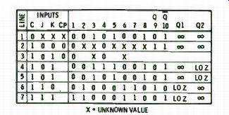
Fig. 2-17. Analysis table for Fig. 2-16.
... 0 and, thus, transistor Q1 is nonconducting at this point; its collector is "hanging" and both inputs to Gate 9 are high, making Q = 0. ( If the Clock should go low while Clear = 0, transistor Q1 still does not conduct, since Gate 7 is 0. Transistor Q2 would conduct, since the output of Gate 8 is 1, and this would cause a second 0 to appear at Gate 10. Thus the state of the Clock is irrelevant.) Also, the state of the J and K inputs are irrelevant.
In line 2, Fig. 2-17, Clear is 1 and J = K = 0. With J = K = 0, Gates 1 and 4 are 0. Gates 3 and 6 are not controlled by Gates 1 and 4 and are indeterminate. Thus, the flip-flop stays locked in whatever state it was in.
Let a clock signal with the waveshape shown in Fig. 2-18 be applied. At point 1 on the waveform, the slave part ( Gates 9 and 10) of the circuit is isolated from the master part of the circuit because transistors Q1 and Q2 become open circuits as their emitter voltages are raised toward their collector volt ages. With transistors Q1 and Q2 open ( infinite impedance), Gate 9 and 10 have these inputs "hanging," which is the equivalent of applying a 1. Since a 0 is the controlling f 'friction in a NAND gate, Gates 9 and 10 are no longer affected by what happens in the master part of the circuit, as long as the clock voltage remains above point 1.
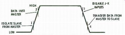
Fig. 2-18. Clock waveform for Fig. 2-16.
At point 2 on the waveform, the clock voltage has risen far enough to remove its inhibiting effect on Gates 1 and 4. however, with J = K = 0 (line 2), Gates 1 and 4 remain a 0, and the flip-flop remains in its previous state. As long as the clock voltage stays above point 2, the circuit is susceptible to changes in J and K inputs; normally the J and K inputs will not be changed during this period. As clock voltage falls below point 3, Gates 1 and 4 are again inhibited, thereby disabling the J and K inputs. At point 4 on the waveform, transistors Q1 and Q2 are again enabled; if Gate 7 is high, transistor Q1 will conduct and put a 0 on Gate 9. If Gate 8 is high, transistor Q2 will conduct and put a 0 on Gate 10. In the case just considered, no change has occurred in the master flip-flop, so transistors Q1 and Q2 resume their previous state-one conducting and one open.
In line 3, let J = 0 and K = 1. With the clock = 0, Gates 3 and 6 are not affected. The clock waveform is applied, and at point 1 the slave is isolated from the master. At point 2 ( line 4) , the inputs are enabled, and since J = 0, Gate 1 = 0 but Gate 3 is still indeterminate-that is, not controlled by input J alone. Gate 4 has the clock and K inputs of a 1 and, thus, its output will depend on the state of its third input (which is the Q output of the slave flip-flop) . If Q happens to be a 1, Gate 4 will be a 1, and this will drive Gate 6 to a 0. Gate 2 has a 0 and a 1 for inputs and goes to a 0, causing Gate 3 to have two 0 inputs and go to a 1. Gate 7 is driven to 0 by Gate 6. Gate 8 has one input 1, with the second connected to the collector of transistor Q1. Since transistor Q1 is open at point 2 and above on the waveform, Gate 8 has both inputs a 1 and thus is a 1.
At point 3 on the waveform shown in Fig. 2-18, the J and K inputs are disabled, but this does not affect Gates 2, 3, 5, 6, 7, and 8.
At point 4 on the waveform, the transistors are enabled.
Since Gate 8 = 1, transistor Q2 conducts, thus putting a 0 on one input of Gate 10. With one 0 input, Gate 10 goes to 1, (making CI = 1), which in turn gives Gates 9 one input = 1 and one "hanging" input, so Gate 9 goes to 0. Thus, Q goes to 0 in agreement with the truth table.
In the discussion above, we assumed that Q was a 1. What happens if it is 0?
Line 5 shows that the result is exactly the same. At point 1 on the waveform shown in Fig. 2-18, the slave is isolated. At point 2, data is entered into the master.
Gate 1 with J = 0, stays at 0. With Q = 0, Gate 4 has one input 0 and thus is 0. However, for Q to be a 0, both inputs to Gate 9 must be a 1. Thus, input B to Gate 9 must be a 1, which in turn requires that Gate 7 be a 0. (With its base voltage 0, transistor Q1 will be cut off, making input 9B =1.) For Gate 7 to be a 0, its B input must be 0, which in turn requires that Gate 6 be 0. If Gate 6 is 0, Gate 3 = 1. Thus, when J = 0 and K = 1, the circuit goes into the Q = 0 state, regardless of its previous condition.
The next condition is when J = 1 and K = 0.
The circuit is symmetrical except for Gates 2 and 5. Since the Clear input to Gate 2 is a 1 in normal operation, Gate 2 acts exactly like Gate 5. The circuit will thus perform as described previously, except Q always ends up as 0, and Q ends up as 1.
The final case is when J = K = 1. Consider the circuit when Q = 1. At point 2 on the waveform, Gate 4 is 1 and Gate 1 is 0 (since Q = 0). Gate 6 is driven to 0 and Gate 3 is driven to 1.
When Gate 3 = 1 and Gate 6 = 0, the circuit will, as we have seen previously in lines 4 and 5, end up in the Q = 0 state at the end of the clock pulse.
Consider circuit operation when Q = 0 ( line 7). Now at point 2, Gate 4 goes to 0 and Gate 1 goes to 1. Gate 3 goes to a 0 and Gate 6 to a 1. This set of conditions drives Q to a 1 at point 4 of the waveform. Thus we see that the circuit toggles every time a clock pulse enters.
OTHER VERSIONS The logic diagram shown in Fig. 2-16 is for the circuit type SN5473/SN7473 manufactured by Texas Instruments. The same part, as manufactured by Motorola, does not use Gates 5, 7 or 8. Gates 3 and 6 are allowed to switch transistors Q1 and Q2 directly, rather than being buffered by Gates 7 and 8.
The buffering and circuit symmetry provided by Gate 5 is dispensed with in the Motorola version. The circuits function identically, of course, and are interchangeable; otherwise they would have different part numbers.
In many digital circuits, the J and K inputs to be applied to a flip-flop are not single inputs but are functions of several variables. This gives rise to the so-called ANDed J-K flip-flops.
The Motorola version of circuit type SN5472/SN7472, an RESET 2
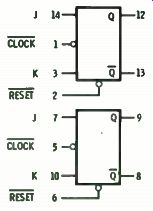
Fig. 2-19. Block symbol for SN5473/SN7473.
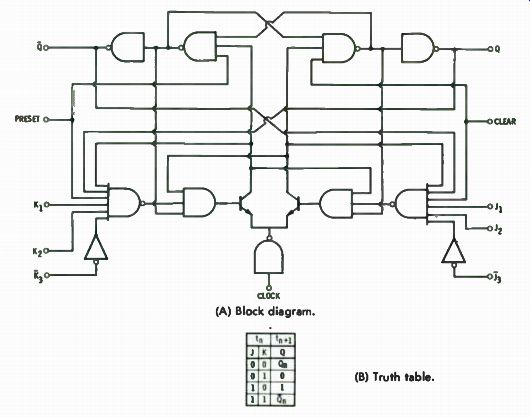
ANDed J-K Master-Slave flip-flop with direct Set and Reset, is shown in Fig. 2-20A. Comparing the circuit with Fig. 2-16A (note the interchange of lettering), we see that Gates 7 and 8 are gone, and Gate 5 is symmetrical with Gate 2, thus giving direct Set. For J to be a 1, J1, J2, and J3 must all be 1; this is similar for K.

B) Block symbol. (A) Functional block diagram.
Fig. 2-20. ANDed J- K Master-Slave flip-flop.
The block symbol drawing for the circuit is shown in Fig. 2-20B. The symbol drawing includes the pin numbers of the IC package. Because of the extra pins needed to handle the extra J and K inputs, only one flip-flop goes into a standard package. The block symbol drawing shown in Fig. 2-19 includes two flip-flops, since the SN5473/SN7473 contains two circuits.
Fig. 2-21 shows the block symbol drawing for circuit type 5470/7470. The J* and K* inputs are true when 0. Thus, K = 1 when K1 is 1, K2 is 1, and K* is 0. Inputs J* and K* must be ...
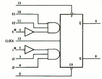
Fig. 2-21. Edge-triggered J- K Master-Slave flip-flop with inverted inputs.
... grounded when not used; otherwise they will present a 0 at the AND gate and lock up the circuit accordingly.
High-Speed J-K Flip-Flop
A J-K flip-flop with a somewhat different operation than has been previously considered is shown in Fig. 2-22. This flip flop is a member of the high speed type 54H/74H family of ...
(A) Block diagram. (B) Truth table.
Fig. 2-22. High-speed monolithic J-K flip-flop.
... circuits and operates at up to 50 MHz. The truth table, however, is the same as for other J-K flip-flops.
Applying a 0 input to the Preset drives Gate 7, and thus Q, to a 1. ( Gate 8 is a buffer amplifier.) With Clear having an input of 1 and the clock low, Gate 9 has all inputs = 1 and, therefore, goes to 0; thus, Q = 0. Applying an input of 0 to Clear sets Q to 0 and, with Preset = 1, Q goes to 1.
Fig. 2-23. Analysis table for Fig. 2-22.
Let's examine the circuit using the analysis table shown in Fig. 2-23. While the clock is low, let J = K = 0 ( line 1) be ap plied ( Clear and Preset = 1). Gates 1 and 4 will be driven to a 1 regardless of the value of Q and Q. If Gate 9 = 0, then the input of Gate 6 (that has the diode connected to the junction of Gates 9 and 10) will see a ground and Gate 6 will be a 0. From similar considerations, Gate 3 = 1. When the clock goes high (above point 1 on the waveform in Fig. 2-24), Gates 1 and 4 stay the same; thus, the circuit does not change when J = K = 0.
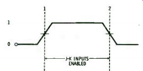
Fig. 2-24. Clock waveform for Fig 2-22.
With J = 0 and K = 1, Gate 4 will be 1 ( line 2 of the table). Assume Q = 1 and Q = 0. For Q to be a 0, Gate 9 must have all inputs = 1. This requires that transistor Q2 be open or cut off; therefore, Gate 6 must be low. For Gate 6 to be low, transistor Q1 must be on. This puts a 0 into both Gate 6 and Gate 7. Gate 1 is high because the clock is low; so Gate 3 has all inputs = 1.
Now, let the clock begin to go high. At point 1 on the clock waveform ( Fig. 2-24), the emitter voltages of transistors Q1 and Q2 has risen sufficiently to cut off these transistors; thus, the inputs to which their collectors are connected see a 1. Gates 7 and 9 are thereby isolated from the input section of the flip flop. At this point Gate 1 will have a 1 on each of its inputs and will go to 0; Gate 3 will go to 0; Gate 4 still has its J input = 0 and will go to 1. Gate 6 will go to 1 because each input is a 1.
Now let the clock go low. As the clock waveform passes below point 2, transistors Q1 and Q2 are enabled. The output ...
(A) Block diagram. (B) Truth table.
Fig. 2-25. Positive edge-triggered flip-flop.
... of Gate 6 is a 1; therefore, transistor Q2 is driven into saturation, which puts a 0 on an input of Gate 9 and Q goes to a 1.
Gate 3 is 0; therefore, transistor Q1 is cut off and Gate 7 sees a 1 on this input. Gate 7 has all is as inputs and goes to 0. Because the slave flip-flop changes state when the clock goes low, the circuit is called a negative edge-triggered flip-flop.
The final mode of operation is for J = K = 1. With the clock high, the gates are as shown in line 5. When the clock goes low, transistor Q2 turns on and 45 is driven from 0 to 1. In line 6,
J and K are 1 but now Q= 1, setting up the gates as shown.
When the clock goes low, transistor Q1 turns on driving Q to a 1 and Q to a 0. Thus, the circuit toggles on the negative edge of the clock pulse when J = K = 1.
Positive Edge-Triggered Flip-Flop
Both the J-K Master-Slave circuit and the high-speed J-K type 74H106 circuit are negative edge-triggered circuits. Type D flip-flops, however, trigger on the positive edge of the clock pulse and so does type 7470, shown in Fig. 2-25.
The key to positive-edge triggering in this circuit is the inverter or NAND gate in the clock input. When the external clock pulse goes high, the switching transistors see a signal going low, and the circuit responds accordingly. Circuit operation otherwise is identical to J-K flip-flops.
Note the inverters of the J3 and K3 inputs. For clocked operation, these two inputs can be connected to the clock input.
If inputs J3 and K3 are not used, they should be connected to ground, which will put a 1 on their respective input gate.
These is free the gates to follow the other inputs.
Prev: BASIC TRANSISTOR-TRANSISTOR LOGIC
Next: DECODERS
Guide Index : Transistor-Transistor Logic (early 1970s)