AMAZON multi-meters discounts AMAZON oscilloscope discounts
Rectifier probes are added to the voltmeters to enable the measurement of r-f, i-f, and video frequencies. Normally they increase the input resistance and decrease the input capacitance of the meter.
Vtvm's are essentially DC indicating devices. The most common is the two-tube bridge type (shown schematically in Fig. 4- 1) , in which a potential unbalance due to application of a voltage to one of the grids causes a difference of potential between the two cathodes. This, in turn, sends a current through the meter.
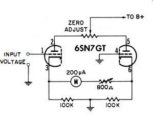
Fig. 4-1 . Basic circuit of a vacuum tube voltmeter.
The DC scales of the meter are linear, but a linear AC scale would also be desirable. Therefore, a linear rectifier is needed, the DC output of which is directly proportional to the applied AC voltage.
A vacuum-tube or semiconductor diode in the probe furnishes this rectification. Although both types of diodes serve the same purpose, each has its advantages and drawbacks. The waveform, frequency, and amplitude of the voltage being measured determine the selection.
If we are interested in measuring the peak value of a signal, the vtvm must have a half-wave peak-indicating rectifier preceding its voltage-divider input circuit. The scale of the vtvm is then calibrated to read peak AC voltage.
The rectifier circuit itself may be built into the vtvm, or contained within the probe ... the operating principle is the same. If the circuit is in the meter, the frequency response is limited to no more than a few megacycles at best. Beyond that, accuracy will drop sharply be
cause of the shunt capacitance from the cable connected to the meter.
The most common rectifier circuit, the shunt type in Fig. 4-2, uses either a vacuum-tube (Fig. 4-2A) or semiconductor (Fig. 4-2B) diode . Some vtvm's contain rectifier circuits which indicate peak-to-peak voltages of all waveforms-including sine waves as well as complex waves and pulses . Peak-to-peak reading vtvm's are particularly useful in the servicing of television receivers because, in addition to the correct waveshape, the service manuals indicate the peak-to-peak voltage values throughout the receiver. Peak-to-peak indicating vtvm's usually have an additional scale showing the rms values of sine-wave signals.
Peak-to-peak indications are obtained by means of voltage-doubler rectifier circuit which, like the half-wave rectifier, is built into the instrument or probe. Here again we may use semiconductor rectifiers or a twin-diode vacuum tube-usually a small high-frequency diode designed for reasonably high voltages, with low plate-to-cathode capacitance.
(A) Using a vacuum tube. (B) Using a semiconductor.
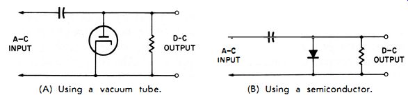
Fig. 4-2. A shunt type diode rectifier circuit.
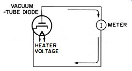
Fig. 4-3. Current will exist in a diode circuit with only heater voltage applied.
Some instruments of their probes permit either peak or peak-to peak indications to be selected by simply flipping a switch.
Fig. 4-3 shows a diode with only heater voltage applied. If a meter is inserted in the plate circuit, a small current will flow from cathode to plate, even though no plate voltage is applied.
This current occurs when some of the electrons which leave the heated cathode manage to reach the plate, even though no positive voltage is present there to attract them. Admittedly, the current is in-deed small. Nonetheless, if there were a resistor in the plate-to-cathode circuit, a voltage drop would be developed across it.
Even if the current is only 25 microamperes, a 20,000-ohm resistor in the plate circuit will produce a voltage drop of one-half of a volt.
This means the plate will now be one-half volt negative with respect to the cathode. Therefore, we would first have to apply one-half volt to the probe-in order to overcome this opposing voltage-before we could get any output indication from the signal under test. Of course, the sensitivity of the probe will then be reduced, particularly at low voltages. We will also get a one-half volt indication on our vtvm, even though there is no applied voltage. This voltage (called contact potential) can be nullified, however, by a bucking (canceling) voltage equal in magnitude but opposite in polarity.
(A) By using a battery. (B) By tapping B+.
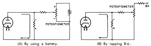
Fig. 4-4. Two ways of obtaining
a bucking potential.
The contact potential of a vacuum-tube diode can be nullified in several ways. The one usually employed in a vacuum-tube voltmeter is to connect one or more dry cells and a potentiometer to the tube in such a manner that we can adjust the pot to deliver a voltage of equal size but opposite polarity to the one developed by the diode. This is shown in Fig. 4-4A. If we want to get away from the problem of replacing dry cells, we can get the same results by tapping a bleeder resistor in the power supply. In Fig. 4-4B, a potentiometer is connected through a voltage-divider resistor to B+. A small positive voltage (with respect to ground) is developed across the potentiometer, the arm of which is connected to the diode plate through an isolation resistor. By proper adjustment of the potentiometer, we can apply a bucking potential which opposes the contact potential developed by the tube. As long as the diode is operating properly, the potentiometer should need no further adjustment.
A third way of neutralizing the contact potential of the diode is to add another diode-either the second half of a twin diode, or a separate tube within the instrument-and use the contact potential of this diode to counteract that of the first. This is explained later in the section.
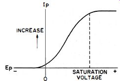
Fig. 4-5. Typical plate-voltage an DC current characteristics of a vacuum-tube
diode.
VACUUM TUBE AND SEMICONDUCTOR DIODES
Although it does have the advantage of being able to handle higher voltages than the semiconductor diode, the vacuum-tube diode requires a filament voltage and a means of compensating for the contact potential it develops. On the other hand, the semiconductor diode not only requires no filament voltage, but also is smaller. Its voltage handling capabilities are usually limited, but its output may be fed directly to the DC voltmeter--no balancing (bucking) potential is needed.
The plate-voltage-plate-current characteristics of a typical diode tube are shown in Fig. 4-5 . Except at the two extremes of the curve, the plate current varies proportionally with the plate voltage . At the top of the curve, the characteristic of a diode is such that any further increase in plate voltage will not proportionally increase the plate current. This point is the saturation voltage of the tube.
It is most desirable for the plate current of the vacuum tube to vary in step with the plate voltage. In this way, when a vacuum tube is used as a rectifier, its output over most of the characteristic curve will be directly proportional to the applied AC signal.
We can avoid the saturation region by limiting the maximum voltage applied to the tube. However, linear output still cannot be obtained at the lower end of the curve when small input voltages are introduced. For this reason, the 1-, 3-, and sometimes the 5-volt ranges are nonlinear on a vtvm containing a vacuum-tube rectifier.
The vacuum-tube diode in a probe should have the lowest possible plate-to-cathode capacitance and the highest possible input resistance, in order to offer a high input impedance to the circuit under test.
Special diodes are available which have all the desirable characteristics for use in high-frequency probes. The chart in Table 4-1 compares the characteristics of vacuum-tube and semiconductor diodes .

Table 4-1. Comparison of vacuum-tube and germanium diode characteristics
-------------------
Vacuum-Tube Diodes |
Develops contact potential which must be compensated for.
Emission affected by line voltage.
High-frequency response limited by transit time.
Maximum input voltage is usually 200 to 500 volts.
Momentary overload usually doesn't cause permanent damage.
Is stable over wide temperature range Tubes can be easily replaced. Usually no selection, only changing required.
Response becomes very nonlinear below one volt due to curvature of characteristic curve.
----
Germanium Crystal Diodes
Develops no contact potential.
No such problem.
High frequency response better than for tube.
Maximum input voltage of most crystal probes is 28 volts peak.
Voltage overload usually destructive.
Affected by changes in temperature.
Diodes may have to match meter scale and instrument calibration.
More linear response than tube at low voltage levels.
---------------------
Semiconductor diodes are very small compared to vacuum tubes . For this reason, the elements do not have much capacitance and series inductance. So, we gain the advantage of a very good frequency response. There are a few commercial probes which, by using the frequency-response characteristic to the utmost, permit measurements in the gig ACycle range.
Fig. 4-6 shows some vacuum-tube and semiconductor diode symbols and how to identify their polarities.
When an AC voltage is applied across a semiconductor diode, current will flow during one half of each cycle. During the other half the semiconductor diode will present a much higher resistance. This is its inverse resistance. The ratio between these two resistances should be at least 1000: 1. In most vacuum tubes, the inverse resistance of around two to ten megohms is so high, compared to the shunt resistance across the circuit, that we can ignore it. In a semiconductor diode, however, it may drop as low as several thousand ohms. Since the inverse resistance and the input circuit of the probe are essentially in parallel, the input impedance of the probe may be seriously reduced at low frequencies. (Keep this fact in mind when measuring low-frequency signals with a probe containing a semiconductor diode!)
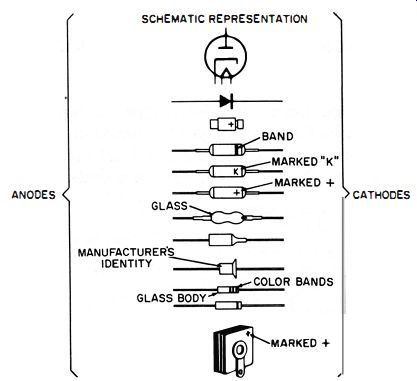
Fig. 4-6. Representations of a vacuum-tube, germanium, silicon, and selenium
diodes.
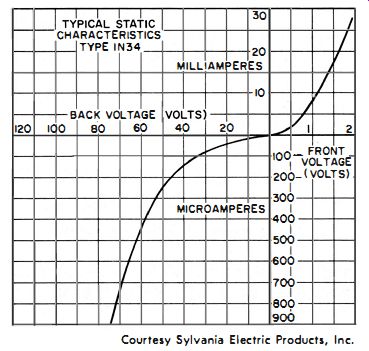
Fig. 4-7. Static characteristics of the 1 N34 germanium diode.
The characteristic curve of a IN34 diode (Fig. 4-7) is similar to that of a vacuum tube at the lower portion, becoming essentially a square law curve below one volt. Unlike the vacuum tube, however, the semiconductor diode has zero current at zero volts. The reason is that we do not have the contact-potential problem we had with the vacuum tube, since there are no electrons being propelled by thermionic emission.
(A) Signal rising in positive direction.
(b) Signal dropping from positive to zero.
(C) During negative half of cycle.
(D) Signal going from zero to positive peak.
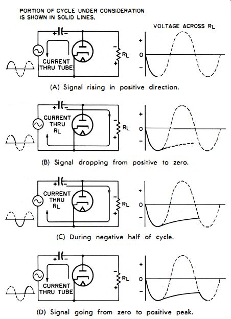
Fig. 4-8. Operation of a shunt-type rectifier.
PEAK-READING, SHUNT-TYPE RECTIFIERS USING VACUUM TUBES
A rectifying probe raises the high-frequency range of the meter being used. The probe functions as an r-f detector to provide a rectified output voltage proportional to the peak value of the voltage detected.
First, let us discuss the circuit of the peak-indicating, shunt-type rectifier employing a vacuum-tube diode. Its DC output is equal to the peak value of either (but not both) half cycles of the applied AC input voltage.
Fig. 4-8 shows the simple circuit for a shunt diode rectifier. It has an AC input voltage (which, for simplicity, we will assume to be a sinewave) and a load resistor, R1 across which we get our output voltage.
RL may be split up into two resistors and the output taken across only one of them. For ease of explanation, we will use only one resistor now.
When the input voltage first swings in a positive direction (Fig. 4-8A), the plate of the diode also becomes positive with respect to the cathode. The tube then conducts and thereby acts as a low resistance in parallel with R1. During the first half of the positive cycle, the increasing positive plate voltage attracts electrons through the tube, to the side of the capacitor connected to the plate. The capacitor is thus charged to the peak value of the applied voltage ; the polarity of this voltage is such that the side connected to the plate is negative with respect to the side connected to the input signal . As the voltage drops from its peak value during the second portion of the positive cycle (Fig. 4-8B), the tube does not conduct because its plate is negative with respect to its cathode. Now the tube acts as a high resistance across the circuit, so the capacitor begins to discharge through RL. The resistance of R1 although relatively high, is still lower than that of the tube when not conducting. So the discharge will take place rather slowly and will follow the shape of the standard discharge curve of a capacitor. The time constant of this circuit is made so long that, even at low frequencies (and here, the lower frequency limit is determined partly by the size of the capacitor), very little of the capacitor charge will leak off through the resistor before the current flows through the tube, again recharging the capacitor.
As the input signal passes through zero and into the negative half-cycle (Fig. 4-8C), the capacitor will continue to discharge through the resistor. There can be no further conduction through the diode because its plate is still negative with respect to its cathode. The input signal again goes through zero and in the positive direction (Fig. 4-8D) . When the input voltage exceeds the level to which the capacitor has discharged through the load resistor, the plate becomes more positive than the cathode and the tube conducts, again charging the capacitor to the peak value.
After the first cycle, the circuit will assume a steady-state condition . The only current will consist of pulses--each lasting only a tiny fraction of a cycle-through the diode during positive peaks of the input signal, as shown in Fig. 4-9. The plate resistance is infinite while the tube is not conducting. This infinite resistance, plus the fact that the load resistor is usually many megohms, is the reason for the extremely high input impedance of the circuit. Any or all of the capacitor charge that leaks off through the load resistor while the tube is not conducting is applied to the vtvm. The voltage drop across RI. is directly proportional to the charge on the capacitor. Therefore, the DC voltage output is a direct indication of the peak value of one-half cycle of the applied AC voltage . In addition to functioning as a charging capacitor for the rectifier circuit, the input capacitor also blocks any direct current, to prevent it from reaching the diode. Therefore, measurements can be made at the plates and grids of vacuum tubes, where a DC voltage also accompanies the AC signal.
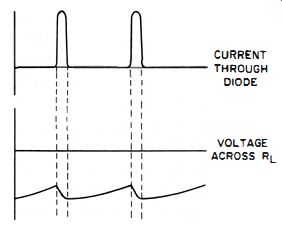
Fig. 4-9. Current pulses through diode after several cycles of input signal
have passed.
Because of the way the diode is connected in Fig. 4-8, the meter indication will be proportional to the positive peak voltage of any signal applied. The diode will conduct during the positive half-cycle only ; there will be no conduction during the negative half-cycle, regardless of any excursion in that direction. If we ground the plate and connect the cathode to the capacitor, we will get an indication during the negative peak value of the input voltage only. The tube operates exactly as before, except now it conducts during only the negative peak of the input signal. Of course, the plate is still made positive (with respect to the cathode) before the tube conducts.
When the rectifier is in a separate probe connected to the vtvm with a shielded cable, the shield or ground will be positive with respect to the vtvm input terminal if this tube is connected as shown in Fig. 4-8. If we reverse the tube-that is, ground the plate and connect the cathode to the capacitor-the shield will be negative with respect to the input terminal. In a zero-center vtvm, the needle will swing to the left or right, depending on the polarity of the probe output voltage.
On most vtvm's, however, the zero is on the left side of the dial . By setting the polarity switch on the front panel, we can make the needle read upward, regardless of whether a positive or negative voltage is applied.
From Fig. 4-9, we can see that the capacitor charges through the tube during only a very short portion of the input-voltage cycle. During the remainder of the cycle (which is many times longer) , the capacitor discharges through the resistor. The rather low average current through the vacuum tube results in a very high input impedance for the probe. By maintaining a low shunt capacitance and limiting the current through the tube to a small portion of the cycle, we present a high impedance to the circuit under test. This, of course, means less loading than if there were a large distributed capacitance and a more continuous current through the diode.
During each cycle of the input voltage, the capacitor is quickly charged, but only partially discharged. Therefore, the time constant of the input capacitor and the load resistor must be made as long as practical, so the capacitor will discharge as little as possible between peaks of the input voltage. In this way, the DC level can be maintained equal to the peak input voltage.
In Fig. 4-10 we see that with a given time constant, the output voltage depends on the frequency of the input signal . The time constant must therefore be chosen so the shunt capacitance is kept low for the higher frequencies. Yet the time constant must be long enough that low-frequency voltages can also be measured satisfactorily. It is obvious that the value chosen for the capacitor must be a compromise . Usually it is such that the time constant of the RC network is approximately 100 times the reciprocal of the lowest frequency we wish to measure. This is given by the following equations: where,
1 T = I
T is the time for one cycle of the input signal, f is the frequency of the signal in cycles per second.
The time constant of an RC circuit equals R times C (where R is the resistance in megohms and C is the capacitance in microfarads) ; RC must equal 100T. Therefore, by substitution,
RC
= 100 xi fRC = 100 C
= 100 fR
(A) High-frequency signal. (B) Low-frequency signal.
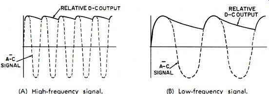
Fig. 4-10 Effect of the input-signal frequency on the rectifier output.
If the value of the capacitor is too small, or if the frequency to be measured is lower than the one chosen for our capacitor value, the meter indication will be low because the capacitor will lose too much charge between peaks of the input voltage. Therefore, the average voltage across RL will be lower than the peak input voltage.
Let us consider the relationship between time constant RC and the charge remaining in a capacitor at various times during discharge.
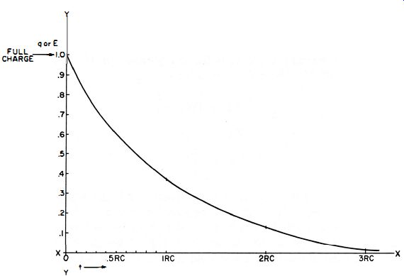
Fig. 4-11. Discharge curve for an RC circuit.
This relationship is shown by Fig. 4-11 , where the charge is plotted vertically and time (t) horizontally. Notice that the X axis is divided into RC units, not seconds-that is, 0. 1RC, 0.2RC, 1RC, and so on.
Although the co-ordinate for any value of t can be found by formula, we will not give it here, but may quote values obtained by its use.
The formula enables us to find the charge remaining on the capacitor after one cycle of discharge. This can be done for any RC product or any signal frequency. For example, suppose we choose a specific signal frequency and design a probe to meet the requirement of RC = 100T. How closely will the output voltage match the input voltage? Rearranging the formula, we get T = RC + 100. The corresponding value for t in Fig. 4-11 would be RC + 100, or 0.01RC, except for one fact : t in Fig. 4-11 represents the discharge time entirely ; T, the duration time of one complete input cycle, is therefore half charge and half discharge time. For this reason, we must use the formula, t = 0.005RC. This value is too small to be read on the curve of Fig. 4-11. but, if substituted in our absentee formula, yields 0.9952--the charge remaining at the end of the cycle . In other words, the charge on the capacitor has dropped less than one-half of one percent.
Thus, the formula RC = 100T gives us a negligible loss. In fact, a figure of RC = 10T might sometimes be acceptable. The latter would give a loss of not quite five percent.
Let us see what value of RC would be necessary for a probe de signed to pass 60 hz-first for RC = 100T, and then for RC = 10T. (1) At 60 hz, T = 1 -;- 60 and RC = 100 -;- 60. If we choose 10 megohms for R, then C must be approximately
0. 17 mfd. If R is 20 megohms, then C can be half as large, or
0.085 mfd.
(2) RC = 10T and T = 1 -;- 60; therefore, RC = 10 -;- 60. If R is 10 megohms, C will be .0 16 mfd; and if R is 20 megohms, C will be 0.0085 mfd.
Frequencies lower than 60 hz would result in a greater loss, which becomes smaller at higher frequencies. Therefore, the probe is good for all frequencies above 60 hz (up to the point where distributed circuit capacitance begins to take effect). For lower frequencies, however, we must accept more loss.
Besides the characteristics of a probe at higher frequencies, we must be concerned with those of the material in the probe, plus skin effect and the transit time of the tube. To keep the dielectric losses as low as possible, those portions of a tube carrying r-f energy are usually protected by polystyrene or other good r-f insulation. Skin effect (where the higher-frequency currents travel close to the surface of a conductor instead of through it) can be greatly reduced by making the r-f-carrying circuit-in other words, the probe tip and the capacitor leading to the diode-as short as possible. Transit-time difficulties can be lessened, up to several hundred megacycles, by using the tiny ultra-high-frequency diode tubes designed for this purpose.
One of the more important requirements for a high-frequency probe is that it exhibit the lowest possible shunt capacitance. Why this is true can be understood from the fact that at 100 megacycles, for example, the reactance of a 10-pf capacitance is only 160 ohms.
The probe itself not only must have a low input capacitance, but also must not introduce additional stray capacitance when connected to the equipment under test.
(A) Second harmonic in phase. (b) Second harmonic out of phase.
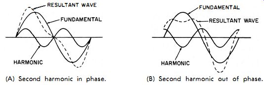
Fig. 4-12. Effect of the second-harmonic phase on the fundamental waveform.
So far we have dealt with sine waves only. But if the input voltage contains harmonics, our meter indication may differ (sometimes even greatly) from the rms value. The amount will depend on the percentage of harmonics and their phase relationship to the fundamental frequency. Fig. 4- 12A shows the resultant waveform when an in-phase second harmonic is combined with the fundamental; Fig. 4- 12B, when the second harmonic is out of phase. Table 4-2 is an example of the erroneous readings obtained when voltages containing harmonics are applied to an rms-calibrated vtvm. These errors will crop up, regardless of whether the meter is calibrated for peak or for rms voltages.
A peak-reading voltmeter will also give erroneous readings if used to measure an unsymmetrical waveform. Moreover, if a 180-degree phase shift exists (such as at the grid and plate of a tube) , two different peaks will be measured-the positive or negative one at the grid, and a peak of the opposite polarity at the plate. One way of circumventing this problem is to measure peaks of the same polarity at both the grid and plate . This we do by using the polarity-reversal switch on the voltmeter as we check from grid to plate. However, we must also take the electrical characteristics of the signal source into account, so we can be sure such a reversal will not be detrimental .
Transit Time
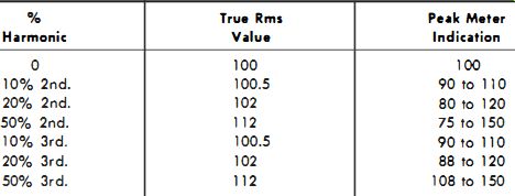
Table 4-2. Measurement errors from harmonic or other spurious voltages.
The frequency of the voltage under test increases until the time (transit time) the electrons take to travel from the filament or cathode to the plate of the diode becomes a noticeable-and often an appreciable-portion of a cycle of the applied input voltage. From here on, the tube characteristics change radically : The electron flow between elements is no longer instantaneous ; nor does it follow exactly the changes in plate-to-cathode voltage. Because the tube is unable to respond faithfully to the changes in amplitude of the input signal, an error is introduced in the output voltage . This error becomes larger as the frequency of the applied signal increases. The plate resistance and the plate-to-cathode capacitance of the tube also change. This is the reason tubes with a short transit time, high self-resonant frequency, and the lowest possible cathode-to-plate inter-element capacitance have been designed.
In the input diode of the vtvm, the amount of error due to the transit-time effect depends on the magnitude and frequency of the applied voltage and on the characteristics of the tube-the latter involving the shape, size, and spacing of the electrodes.
(A) Pulse charging action. (B) Rectifier circuit.
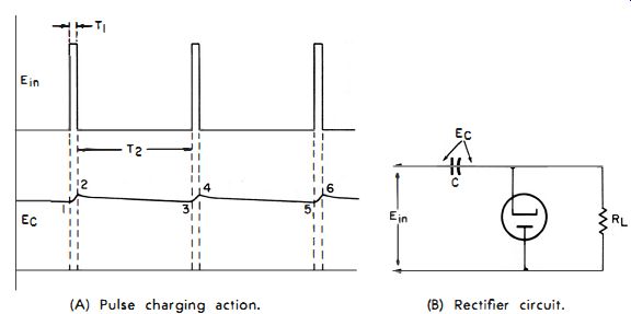
Fig. 4-13. Output-voltage and pulse-width repetition-rate relationship of
the rectifier.
(A) At cathode of vertical output tube.
(C) At horizontal oscillator transformer.
(B) At input to second video amplifier.
(D) At input across horizontal deflection coil.
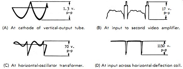
Fig. 4-14. Typical nonsymmetrical voltages encountered in television receivers.
Pulse Response
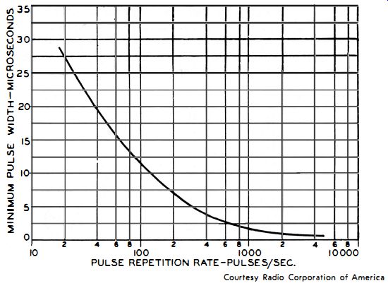
Fig. 4-15. Pulse response of a typical vtvm.
(A) Probe.
(B) Probe circuit.

Fig. 4-16. Model RF·10A peak indicating probe.
(A) Construction.
(B) Circuit.
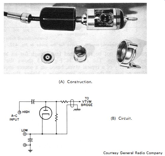
Fig. 4-17. A commercial high frequency peak indicating probe.
Let's examine the pulse in Fig. 4- 13A. Its width, T}, is small compared with the repetition rate, T 2. The tube, which conducts only when pulses are present, will thus charge the capacitor connected across the load resistor. Our meter will read the voltage developed across RL in Fig. 4-13B. The voltage across the capacitor (Fig. 4-13A) has a chance to build up between the very short time interval 1 and 2 only, but has a relatively long time to discharge. The slope of the curve between 2 and 3 will be determined by the time constant of the capacitor and load resistor. If the ratio between time intervals T2 and T1 is small, the capacitor will then have no difficulty charging to the peak value of the applied voltage. On the other hand, if the ratio is high, we will run into a problem. Assume that T:! is 999 microseconds and T 1 is 1 microsecond. During this 1 microsecond, the tube must therefore pass the total current drawn by the load during the entire 1000 microseconds from pulse to pulse. So the instantaneous current drawn from the source is 1000 times the current required by the measuring circuit. Moreover, because of transit-time difficulties, the slope from point 1 to 2 may not be steep enough to fully charge the capacitor to the peak applied voltage. Therefore, the capacitor charge at point 3 will also be reduced. As a result, the reading will be below the actual peak value.
When servicing a television receiver or other complex electronic equipment, we encounter many nonsymmetrical and nonsinusoidal voltages like the ones in Fig. 4-14. As you can see, the pulses are narrow and widely spaced-in other words, they have a low repetition rate. Before we can obtain an accurate indication of their peak or peak-to-peak values, we must remember that a relatively constant charge must be maintained on the capacitor between input-voltage peaks . If these peaks are short and very widely spaced, the charge on
the capacitor may not be replenished fast enough for an accurate peak-to-peak reading. The curve in Fig. 4-15 shows the pulse response capability of a typical vtvm, based on a source impedance of 50 ohms or less. If the source impedance is higher, the measurement error will increase proportionally.
The pulse-response capability of a peak or peak-to-peak measuring circuit is determined by the time constant of a resistor and capacitor.
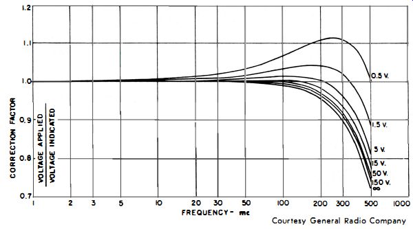
Fig. 4-18. Frequency-correction curve for the probe in Fig. 4-17.
Therefore, we can measure pulses with a low repetition rate and a narrow pulse width by increasing the value of either the capacitor or the load resistor. The load resistor used to develop the output across the grid circuit of the bridge-type vtvm should be as large as possible without causing grid current to flow. The capacitor should also be as large as possible-up to a certain point. Beyond this point the shunt capacitance will be unbearable.
Because of the difficulties encountered when a vtvm is used to measure the peak-to-peak value of a complex wave, an oscilloscope is often preferred for more accurate measurements.
Fig. 4-16A shows the Precision Apparatus RF- 10A peak-indicating probe. It employs a diode-connected subminiature triode, as shown by the schematic in Fig. 4-16B. Meter readings become inaccurate below three volts, and even more so below one volt. Below 200 cycles, a low-frequency correction factor must also be applied. The probe indication is proportional to the positive peak value of the applied AC voltage.
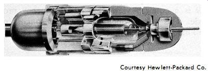
Fig. 4-19_ Internal view of the Hewlett-Packard high-frequency probe used
with Model 41 0-8 vtvm.
Another interesting probe is shown disassembled in Fig. 4-17 A, and schematically in Fig. 4-17B. The instrument to which the probe is attached operates as a peak voltmeter calibrated to read rms values of sine waves. At high frequencies, the meter normally reads high because of resonance in the input circuit. However, the transit-time effect of the acorn diode rectifier tube in the probe causes the meter to read low. At low voltages, the transit time and resonance effects tend to cancel each other. At higher voltages, however, the measuring errors are due almost entirely to resonance.
Courtesy Hewlett-Packard Co.
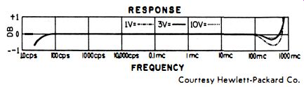
Fig. 4-20. Frequency response of the probe in Fig. 4- 19.
The curve in Fig. 4- 18 shows the frequency correction required for various ranges. At low frequencies, the equivalent input-circuit impedance of the probe is 25 megohms ; but losses due to a shunt capacitance of about 3.1 pf (with the probe cap and plug removed ; 4.3 pf if they are included) reduce the 25 megohms at high frequencies.
When the rotating metal cover of the probe in Fig. 4-17 A is closed, the probe is completely shielded except for the small insulated area.
A metal cap permits various fittings and screws to be attached to the end of the probe . A phenolic cover, held by a nut fastened to a cable strain release, insulates the probe body behind the cap. For high frequency measurements, where the minimum inductance is desirable, a cap can be fastened to a flat ground plate and an axial hole provided for the center terminal.
At low frequencies, the response of this probe drops off because of the increasing reactance of the input circuit (but not more than 2 percent at 20 cycles).
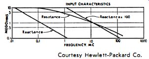
Fig. 4-21. Input characteristics of the probe in Fig. 4-19.
A high-frequency multiplier attachment is available which increases the voltage rating of this probe 10 times.
Fig. 4-19 is a cutaway view of a high-frequency probe using a special diode. This tube, which has a self-resonant frequency of around 1250 mc, places approximately 1.5 pf across the circuit under test. At low frequencies the probe has an input impedance of 10 megohms shunted by 1.5 pf. Its frequency response is flat within ± 1 db from 20 cycles to 700 megacycles. The lower part of this probe is completely enclosed within a grounding shell to aid in establishing a reliable high-frequency ground connection. The Hewlett-Packard probe in Fig. 4-19 is used with the Model 410B vtvm.
As a result of design considerations, the probe has a resonant frequency of approximately 1500 megacycles. The DC output of the probe versus the frequency of the input signal is shown in Fig. 4-20. Note that there are three characteristic curves at the high-frequency end-one each for the 1-, 3-, and 10-volt ranges. At these high frequencies, the response of the probe is affected by (1) the transit time, which depends not only on the frequency, but also on the magnitude of the applied voltage ; and (2) the self-resonant frequency of the probe, which is independent from the voltage under test. The effect of the transit time is shown by a dip in the 1-volt curve in the vicinity of 500 mc. The rise beyond 500 mc can be attributed to the fact that the probe becomes resonant and thereby overshadows the transit-time effect. The input resistance and shunt capacitive reactance of the probe in Fig. 4- 19 is shown in Fig. 4-2 1. At frequencies up to 100 mc, the input resistance is greater than 10 meg-ohms, decreasing at higher frequencies because of dielectric and tube losses and the high-frequency effect of the resistor. The shunt-capacitance component is approximately 1.5 pf and, therefore, the reactance curve varies accordingly.
In a voltmeter probe using a vacuum-tube diode, one of the problems in achieving good stability is the effect of changes in line voltage on the characteristics of the tube. When no plate voltage is applied to the tube, we will still get some contact potential. This contact potential, which transfers a small amount of energy to the anode, is directly related to the filament voltage. Hence, changes in the filament voltage will vary the amount of contact potential . Even though relatively small, this change may nonetheless prove to be annoying when measurements are made at low-voltage levels. If the contact potential of another diode is used to counterbalance that of the active tube (as explained previously), the line-voltage changes will affect both tubes at the same time and in the same direction. Therefore, the change in contact potential will not be so detrimental to the accuracy of the measurement.
A ballast element, sometimes used in the more expensive instruments, regulates the filament voltage supplied to the rectifying diode.
In this way, a more constant voltage can be maintained over a rather wide variation in line voltages.
(A) Responds to negative peaks only. (B) Responds to positive peaks only
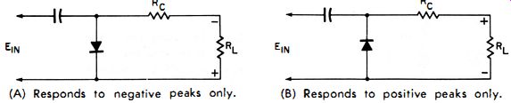
Fig. 4-22. Shunt type peak reading rectifier probes using germanium diodes.
PEAK-READING SHUNT-TYPE RECTIFIERS USING SEMICONDUCTOR DIODES
The circuit of a semiconductor diode probe (Fig. 4-22) is similar to the one employing a vacuum tube mentioned before, in which the peak value of the input voltage is developed across the input capacitor. The same time-constant relationship also holds true for the semiconductor diode-except for one slight difference. When we calculate our time constant, we must remember that the back resistance of a semiconductor diode is not infinite. For this reason, and because the diode is in parallel with the load resistor, some of the capacitor charge leaks off through the diode. We would therefore need a somewhat larger capacitor in order to minimize errors at low frequencies.
When the diode is connected as shown in Fig. 4-22A, the output of the probe is negative; so the vtvm must be set for negative DC volts.
If we reverse the diode (as shown in Fig. 4-22B), the output will be positive, and now the meter must be set for positive DC volts.
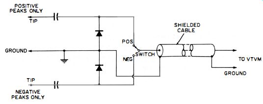
Fig. 4-23. A peak-indicating probe which will read either the positive or
the negative peak, depending on the switch setting.
The two probes in Fig. 4-22 can be combined, giving one which, by means of an spst switch, can measure either the positive or negative peak of a signal. Its circuit is shown in Fig. 4-23. In order to be completely symmetrical, this probe should be made with two individual tips and identical circuitry, except that the cathode of one diode and the anode of the other are grounded. This gives a choice of positive or negative peak indication, allowing us to measure the positive or negative half-cycle of an unsymmetrical signal.
The signal-handling capability of a probe can be increased by connecting two or more rectifiers in series, as shown in Fig. 4-24. Not only is the voltage-handling capability of the probe increased, but also the input impedance, because the back resistances and shunt capacitances of the diodes are now in series. With two diodes, the voltage-handling capability and shunt resistance are doubled, and the shunt capacitance is one-half. With three diodes ... tripled and one-third-and so on for each additional diode.
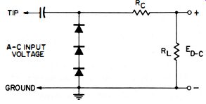
Fig. 4-24. Using more than one diode in series to increase the input impedance
and voltage-handling capability of a probe.
The applied AC voltage must never exceed the voltage rating of the semiconductor diode ; nor should the DC component exceed the voltage rating of the blocking capacitor. The highest operating frequency of a probe is determined not only by its self-resonant frequency, but also by the spacing of its components and leads. The input impedance of a well-designed shunt-type peak-indicating probe is usually over 250,000 ohms, up to 1 megacycle ; and over 5000 ohms, up to 250 megacycles.
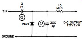
Fig. 4-25. Capacitive divider method of in· creasing the voltage capability
of a probe.
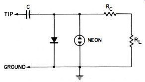
Fig. 4-26. Using a neon bulb to protect the diode against damage from overloads.
It is possible to increase its r-f voltage-handling capabilities by shunting the probe with a capacitor to form a capacitive divider with the input charging capacitor. The circuit (Fig. 4-25) has a 100:1 voltage division. This is suitable for measuring up to 2500 volts, because the voltage across the semiconductor will not exceed 25 volts-still a safe value for our diode.
To prevent a voltage overload from burning out the diode, it can be shunted with a neon bulb, as shown in Fig. 4-26. The bulb will light during an overload and thereby keep the voltage down to a safe level until the overload has been removed. The ionization level of the bulb must be lower than the maximum rated voltage of the diode.
Fig. 4-27 shows the schematic of a high-frequency probe designed for a vtvm having an input resistance of 10 megohms. The frequency response of this shunt-type peak-indicating probe is fiat within ±10 percent, from 20 khz to 100 mc ; and the indication is proportional to the positive peak of the applied voltage.
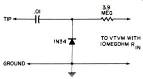
Fig. 4-27. A high-frequency peak-indicating probe for use with a vtvm having
a 10· megohm input resistance.
Fig. 4-28. This crystal diode-detector probe is slipped over the regular DC
isolation probe for which it was designed.
The crystal diode-detector probe in Fig. 4-28 is slipped over the regular DC isolation probe of the RCA Model WV-98A vtvm, for which it was designed. Obviously, no additional lead is required to the meter. The probe extends the frequency range of the vtvm to 250 megacycles. It can be used in circuits where the DC voltages do not exceed 250 volts and the AC voltages are not more than 20 volts rms or 28 volts peak.
(A) The probe. (B) Probe circuit.
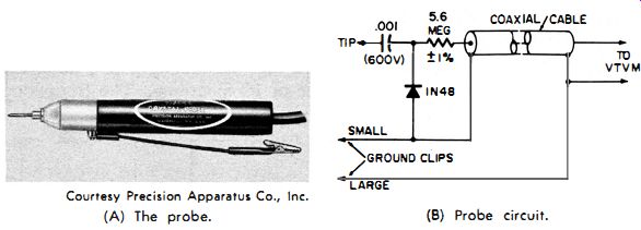
Fig. 4-29. A typical commercial peak indicating probe.
Fig. 4-29 shows another interesting probe . The 5.6-megohm series resistor is chosen to give rms indications on the vtvm for a sinusoidal input voltage. Designed for a frequency range of 50 khz to 250 mc, the probe is accurate within ±10 percent. On the 3-volt range, a correction must be applied. The probe has a shunt capacitance of approximately 3 pf when the small ground clip is attached. A second ground clip, from the connector can be used for measuring frequencies below 200 khz. The equivalent shunt resistance is approximately 200,000 ohms at 50 khz, decreasing as the frequency increases. A compensated X10 multiplier (Fig. 4-30) can be used to extend the usual AC voltage range to 300 volts rms. The probe tip must be unscrewed, replaced with the multiplier head, and the tip screwed into the other end of the multiplier. Do not forget that all scale readings taken with the X10 multiplier head must be multiplied by 10 before the actual voltages can be read. The X10 multiplier head also lowers the input shunt capacitance and raises the equivalent shunt resistance.
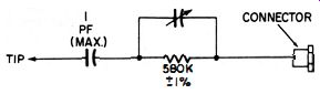
Fig. 4-30. A X00 multiplier for the probe in Fig. 4·29.
PEAK-READING, SERIES-TYPE RECTIFIERS
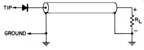
Fig. 4-31 . Basic circuit of a peak-reading series-type rectifier probe.
Fig. 4-31 shows about the simplest version of a peak indicating probe-a semiconductor diode connected in series with the center conductor of a shielded cable . The capacitance of the cable, acting as the charging capacitor, charges to the positive or negative peak value of the applied voltage (depending on the way the diode is connected) . Even though very simple to make, this probe has its faults. At certain frequencies, the shielded cable may act as a resonant stub. The way to circumvent this difficulty is to insert a charging capacitor and a resistor, and then let the cable capacitance act as an additional capacitor to smooth out the peaks. (This is shown in Fig. 4-32.) The resistor can also act as a calibrating resistor so that either peak or rms readings can be obtained with the vtvm. If the diode is connected as shown in Figs. 4-3 1 and 4-32, the output voltage will be positive and there will be a positive voltage on the center conductor of the cable going to the vtvm. If the diode is reversed, the center conductor will of course have a negative DC voltage.
No blocking capacitor is shown because these probes are suitable only for low-level AC measurements where no (or a very low) DC component is present. If there is a DC component and its direction and magnitude are such that it cuts off the diode or overrides the signal, we may get no indication at all. Moreover, if the signal is larger than the reverse bias voltage, our indication will be considerably lower than the actual AC voltage. The reason is that the DC voltage biases the semiconductor diode into the nonconducting region, so this bias voltage is exceeded only during the extreme peaks of the AC signal.
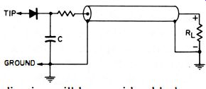
Fig. 4-32. Adding a charging capacitor and
a resistor to the base circuit will improve its performance.
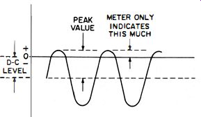
Fig. 4-33. Measuring error introduced when alternating current is measured
in a circuit that also contains direct current and no DC blocking capacitor
is used.
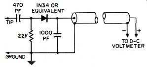
Fig. 4-34. A rectifier probe suitable for a vom with a sensitivity of 5000
ohms per volt or higher.
(See Fig. 4-33.)
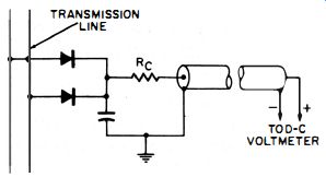
Fig. 4-35. A probe suitable for measuring a balanced circuit.
There is, however, an advantage to this arrangement-we have about the least shunt capacitance we could possibly hope for with a rectifying probe . Here is why. The approximately 1-pf shunt capacitance of the semiconductor diode is in series with the considerably greater shunt capacitance of the cable (or charging capacitor, if used) . Since the sum of any two capacitors in series is always less than the smaller of the two, the equivalent capacitance is less than 1 pf. To that, however, must be added the distributed capacitances from the operator's hand, the shielded cable, and the proximity of the probe to the ground or return of the circuit being measured. Nevertheless, the shunt capacitance is lower than with most any other rectifier probe . A semiconductor-diode probe can also be used with a vom to extend the AC frequency response of the meter beyond that of the built-in rectifier. Such a probe circuit is shown in Fig. 4-34. The meter should have a sensitivity of at least 5000 ohms per volt-and preferably higher. The output terminals of the probe are connected to the DC voltage terminals of the voltmeter. Since the input resistance of the meter is rather low (only 15,000 ohms on the 3-volt range of a 5000 ohms-per-volt meter), the rather high load the probe places on the circuit will tend to alter the r-f voltage being measured (unless we are measuring voltages in low-impedance circuits) . For this reason, any indication-although theoretically that of the peak voltage under test--will be only of voltage present, rather than actual measure. This is due to the circuit loading effect of the probe . With low-impedance circuits, however, we can actually calibrate the probe with a known voltage and thereby get meaningful measurements.
If we want to measure in a balanced-to-ground circuit (in a twin-lead transmission line, for example), we can add another diode, as shown in Fig. 4-35. We now have a double-ended probe we can apply directly across the transmission line to measure, with the least shunt capacitance, the voltages on the line. The diodes are connected in the same direction because, at any point across the line, the polarity of the voltage alternates at the operating frequency. As a result, first one diode will conduct, and then the other. The charging capacitor thus receives two pulses-one each time a diode conducts . As before, resistor R, isolates the probe from the circuit, it can also be used as a calibrating resistor.
Rectifier Probe Selection and Use
Two important considerations in the selection of a probe are the range of frequencies to be measured and the type of voltage to be applied. Even though more suitable than vacuum-tube types at higher frequencies (there are some exceptions, however!), semiconductor probes have a more limited voltage-measuring range. Fig. 4-36 shows a 500-volt probe useful for obtaining the resonant point of transmitter tank circuits, grid circuits, or other high-voltage r-f circuits. The probe shown responds to negative peaks ; reversing both diodes will result in an output based on positive peaks.
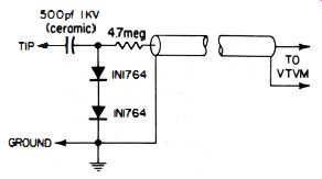
Fig. 4-36. A 500-volt r-f probe.
The 1N1764 silicon rectifiers have a peak inverse voltage of 500 volts each ; thus two of them connected in series permit the probe to be safely used in circuits where the peak voltages are less than 500 volts. The voltage rating of the probe can be raised by adding more diodes . (The peak-voltage rating can be increased by 250 volts for each additional diode.) Since the DC output is proportional to the peak value of the voltage under test, best accuracy will be obtained when the input voltage is sinusoidal. The series resistor is selected for an rms indication for sine-wave input. Fig. 4-37. Output accuracy of the probe shown in Fig. 4-36 as related to frequency and level of the input voltage.
Fig. 4-37 shows that for frequencies from 5 khz to 50 mc the greatest accuracy with this probe is obtained at voltages greater than four volts.
Before taking any measurements, we must of course have an idea of what kind of signal we have and what indication we want. If we have a sine wave, a peak-indicating meter can give us peak or rms readings. On the other hand, if we have a nonsinusoidal wave, only peak-to-peak readings would indicate what we have. The voltage level being measured must never be higher than the maximum rating of the semiconductor diode, or several hundred volts for a vacuum-tube diode (except high-voltage rectifiers) . In addition, the probe must have facilities for making a good ground connection close to the circuit under test.
Voltmeters with built-in rectifiers have a limited high-frequency range, because the large shunt capacitance of the shielded lead through which the signal is applied greatly attenuates the high frequencies. This is one advantage of having the probe at the end of the cable, rather than in the meter. The meter also loads the circuit under test because of shunting by the cable. Locating the rectifier in the probe rather than in the instrument not only lessens the attenuation of the signal as it enters the meter or scope, but also lessens the loading effect of the meter on the circuit.
The success of a rectifier probe depends on its construction and on the components used. If low-inductance capacitors, good quality resistors, a good insulating material for mounting the components, and shortest possible wiring and leads are used, and if designed to have minimum stray capacitance, the probe will be quite practical for very high frequencies. Many such well-designed probes are available, either as accessories or supplied with the instrument.