AMAZON multi-meters discounts AMAZON oscilloscope discounts
This section is devoted to special-purpose analog meters that are typical of the laboratory instruments now in use.
MODEL 2028 DC MICROVOLTMETER
The first instrument selected for discussion is manufactured by Cohu Electronics, Inc., San Diego, California, and is designated as their Model 202B. The instrument is a combination d-c microvolt meter and amplifier, providing a wide range of measurement and amplification. Fourteen voltage-ranges cover from 300 microvolts full scale to 1000 volts full scale. The zero-center meter face indicates polarity on a mirrored scale which covers all ranges. The amplifier has a maximum gain of 70 db to an output connector on the front panel, providing for its use as a low-drift d-c amplifier with high gain and very high input impedance. A photograph of the unit is shown in Fig. 7-1.
Theory of Operation
A schematic (as well as an overall block diagram) of the Model 202B is shown in Fig. 7-2.
Power Supply Section---The power supply section consists of a transformer with four secondaries and a fused primary isolated from the a-c line by an r-f choke and bypass capacitors. The third wire on the a-c line connects the chassis common ground to earth ground.
The top secondary winding of the transformer provides for properly phased alternating current to drive diodes CR1 and CR2 at the output of the chopper amplifier. The next secondary winding supplies a high-voltage, full-wave rectifier the output of which is connected across two series-connected voltage regulator tubes. The point to which the two tubes are connected is grounded. This divides the voltage to provide -105 volts and +150 volts. The third winding supplies a-c heater voltage to all tubes (except VI ), pilot-light voltage, and properly phased energizing voltage to the chopper. The bottom secondary winding supplies heater voltage which is rectified by two 1N91 diodes, supplying direct current to the heater of the first a-c amplifier tube (VI). This minimizes hum pickup in this low-level amplifier.
The Amplifier System---The amplifier system actually consists of two amplifiers : a chopper amplifier and a d-c amplifier. The chopper amplifier is on the input side and feeds the d-c amplifier on the output side. The chopper amplifier is more stable for amplifying low-level direct current than a straight d-c amplifier.
Courtesy Cohu Electronics, Inc.
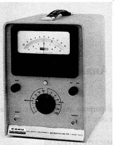
Fig. 7-1 . Cohu Electronics Model 2028 micro-voltmeter.
To prevent oscillation due to feedback loops created by minute voltage differentials between various chassis areas, all grounds in the amplifier are connected to a circuit common ground at the input; they are also brought out to an external earth ground through a third lug on the a-c power plug.
Since the microvolt-meter must indicate the magnitude of extremely small d-c signals, great amplification is necessary before the signal can be used to actuate a conventional d-c microammeter movement.
Gain can be rigidly fixed by the use of a large value of feedback, thus adapting an electronic amplifier for measurement purposes. A conventional direct-coupled d-c amplifier cannot be used, however, because of the trouble encountered with drift and grid currents. If grid current is allowed into the input system, an apparent input signal is developed which results in an erroneous output. In the conventional d-c amplifier, drift may also be caused by changes in the direct current through the tubes. Such changes can be caused by small variations in heater voltage or by normal tube aging, resulting in a deviation in the emission characteristics of the tubes.
These difficulties may be overcome by the chopper amplifier, since it reduces the effect of grid current in the input circuit and plate current drift to a negligible amount by using coupling capacitors.
Fig. 7-3 shows how the effect of grid currents and drifting plate current would give an erroneous output in a conventional d-c amplifier with very small d-c input and how these effects are overcome with the chopper amplifier. Part A shows greatly magnified plate-voltage drift in a d-c amplifier with the grid shorted to cathode. This plate-voltage drift is due to changes in plate current. Part B shows the same voltage drift, but at a different level, due to current through the grid resistance, thus changing the bias.
Part C shows plate voltages with a small positive d-c voltage applied at the grid. Plate voltage drifts as before, but again at a different level. Note that the plate-voltage change caused by the small input signal is on the same order of magnitude as the changes caused by grid current and plate-current drift. Unless a much larger input signal is used, d-c plate voltage change will not depend on signal-voltage change, and the amplifier will give erroneous readings.
Part D shows plate voltage with small d-c voltage being switched on and off at the grid. Note that while drift is still apparent, the rate of change of the square-wave component is constant.
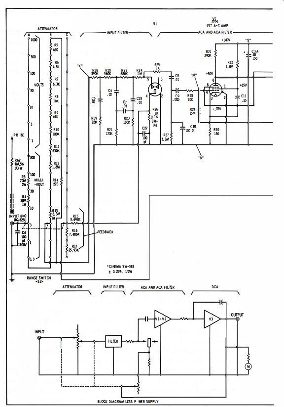
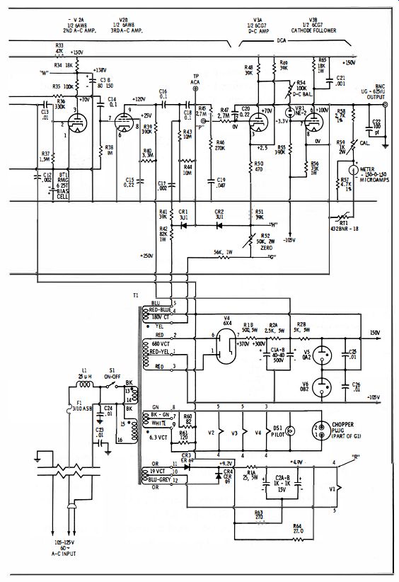
Fig. 7-2. Schematic of Model 2028
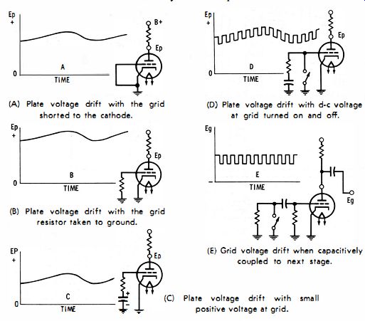
Fig. 7-3. Waveforms showing effects of grid currents and drifting plate current.
Part E shows the voltage of part D as it would appear at the grid of the following stage in a capacitive-coupled amplifier. Since the coupling capacitors have blocked the drifting d-c component, all that remains is for the amplified input square wave to be proportional to the small d-c input. Long-term drift in the system due to thermal effects and circuit aging can be compensated when necessary by the use of a zero adjustment.
The Chopper Amplifier---Fig. 7-4 represents the basic chopper amplifier circuit used in the Model 202B. Its purpose is to convert low-level direct current to alternating current for stable amplification, amplify it, and reconvert it to direct current. The plate decoupling and other circuits that do not directly affect amplification and rectification are not included in Fig. 7-4. For the sake of clarity a synchronously driven output chopper will be used to describe operation of the chopper amplifier, although in the Model 202B a driven crystal-diode system is used to change the alternating current back to direct current after amplification. This will be discussed later.
In Fig. 7-4 the d-c signal to be amplified is represented schematically by a battery in series with a resistor, connected so as to provide a positive input signal. There are two possible positions for the chopper poles at the input and output of the amplifier : poles left and poles right.
With the poles left the input voltage is grounded by the input chopper; the input to the first stage is zero. With no input voltage and assuming a quiet-state plate voltage of 100 volts for the last stage, there is zero output with the output chopper-pole left because the junction of C2 and R6 is grounded and C2 is charged through R5 to the plate voltage (Ep) of 100 volts.
When the input chopper pole goes right, an input of the polarity shown in Fig. 7-4 is applied through C1 to the grid of the first stage.
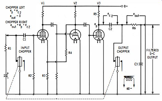

Fig. 7-4. Schematic of basic chopper amplifier circuit.
This results in a decrease in the plate voltage of the first stage, an increase in the plate voltage in the second stage, and a decrease in the plate voltage of the third stage.
Assume that the plate voltage of the last stage drops to 90 volts.
When the output chopper pole is thrown to the right C2 is no longer connected to ground. An output voltage is produced which is equal to the voltage that is now on the plate, minus the voltage level to which C2 was charged just prior to the chopper pole being thrown right. If C2 is charged to a nominal 100 volts and the plate voltage drops to 90 volts because of the positive input signal, the output is then ideally a square wave equal to -10 volts.
Although the input signal is positive with respect to ground, this d-c level is lost through capacitive coupling and except for an initial transient condition the plate voltage of the last stage will vary both above and below the quiet state d-c value. Fig. 7-5 shows input and plate waveforms as they would appear initially and as they would appear after several seconds.
The voltage variation appearing at the plate of V3 would, after passing through C2, vary equally above and below ground potential, giving an average d-c output of zero without further treatment. To obtain a significant d-c output at the junction of C2 and R6, an output chopper must be used. Fig. 7-6 shows the effect of the output chopper on the output waveform at the junction of C2 and R6.
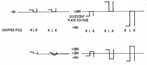
Fig. 7-5. Sketches of input and plate waveforms.
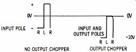
Fig. 7-6. Sketch of output chopper effect on output waveforms.
Fig. 7-6 shows that the output chopper serves to clamp the top of the output square wave with reference to ground. This is accomplished as follows : When the chopper pole goes left the plate voltage of the last stage will rise to + 105 volts and C2 will charge to + 105 volts, being connected between plate and ground. The output voltage will be zero because the junction of C2 and R6 is grounded. When the chopper poles go right again, the plate voltage of V3 will decrease from + 105 volts to +95 volts. Since C2 has no quick discharge path, the output voltage which was zero will drop to -10 volts. Thus the output voltage is again equal to the plate voltage present when the output chopper pole broke away from the left contact.
The voltage across C2 closely follows the plate voltage of V3. This is true since C2 has a relatively fast charge path through R5 and the chopper and a relatively slow discharge path through R6, compared with the half-period of the chopper frequency. Because of this, C2 is unable to discharge to the point that the gain would be affected. It thus becomes apparent that by means of the chopper amplifier a pulsating d-c output is obtained which is proportional to, but larger than, the d-c input.
Note that the d-c voltage gain of the chopper amplifier is less than the a-c voltage gain. If the negative pulsating d-c voltage appearing at the junction of R6 and C2 varies from zero to -10 volts, then its average d-c value is -5 volts. Thus, in this case the d-c voltage gain is half the a-c voltage gain. This is the minimum loss possible. In a practical three-stage chopper amplifier a d-c input to d-c output gain of 10 to 12 db below the a-c gain is to be expected.
The output of the chopper amplifier is filtered by a network designated as R6 and C3 in Fig. 7-4. The time constant of the filter is long compared with a half-period of chopper frequency. The filter actually used in the Model 202B is more complex. In the Model 202B with no signal applied and with the a-c amplifier balanced, there is no output at the filter. With maximum plus d-c signal applied for any range there is a negative d-c output of between 0.1 and 0.25 volt, depending on the amplifier load. The a-c sawtooth ripple is approximately 0.7 volt when measured with the usual averaging-type voltmeter.
Note that in the three-stage, a-c chopper amplifier just described, a phase reversal has taken place in such a way that a positive input voltage -produces a negative output voltage. However, the d-c amplifier which follows produces an additional phase reversal for an overall positive gain with the polarities described. Had the input to the chopper amplifier been negative instead of positive, the direction of all waveforms would have been reversed. The plate voltage on the output stage would have been higher than the voltage of C2 during the period when the output chopper was to the right.
Therefore, the chopper output voltage, which is equal to the plate voltage of V3 minus the voltage on C2 at the time the output chopper switches from left to right, would have been positive. Again, the d-c amplifier would give an additional phase reversal such that a negative input voltage would give a negative indication on the meter. Thus it is seen that with a d-c voltage applied to the chopper amplifier described, a larger inversely proportional voltage appears at the chopper output. This, when further amplified by the following d-c amplifier, gives a d-c output directly proportional to the d-c input.
Driven Diode Chopper---Because of certain design considerations a driven diode system containing 3U l diodes is used in the Model 202B, instead of the synchronous output chopper, to change a-c voltage back to d-c voltage after amplification. The method of utilizing diodes to replace the output chopper is shown in Fig. 7-7. The function of the diodes is similar to that of the output chopper.
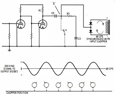
Fig. 7-7. Schematic of driven-diode chopper circuit.
When the polarity of the driving voltage is as indicated in Fig. 7-7, maximum conduction takes place through the diodes and point X is essentially at ground. When the polarity is the reverse of that indicated, point X is isolated from ground.
By proper phasing of the diode a-c supply voltage and the a-c voltage which drives the input chopper, the diodes are in effect synchronized with the input chopper. By using sufficient driving voltage across the diodes, plate resistance is made much lower than would be the case with more conventional rectifiers, and a linear relationship between applied a-c signals and output d-c pulses is obtained throughout the range of the applied voltage. Also, inversely proportional d-c output is obtained, regardless of the polarity of the amplifier d-c input voltage.
The DC Amplifier---As has been discussed, the purpose of the chopper amplifier is to prevent drift and other undesired effects due to grid current, component faults, voltage changes, etc. However, after a number of chopper stages have brought the signal up to a point where the signal to noise ratio is more favorable, circuit economy therefore demands that a direct-coupled d-c amplifier should be employed.
The two-stage d-c amplifier in the Model 202B consists of a triode amplifier and a cathode follower (see Fig. 7-2). A neon bulb is used in the interstage divider to minimize gain loss, since it has low dynamic impedance with a relatively large d-c voltage drop. R54, the d-c balance control, sets the direct-current operating conditions in the amplifier, and the chopper amplifier is not required to furnish a steady bias voltage. The Thyrite resistor across the output and a plate resistor on the cathode follower limit the output voltage and current.
Capacitive feedback is connected between the input and output of the d-c amplifier. The purpose of this feedback is to decrease the necessary size of the filter capacitor, to make system response-time independent of d-c amplifier gain variations, and to minimize the effects of internal disturbances in the d-c amplifier.
Meter Circuit
The meter is connected across the amplifier output in series with the proper multiplier and shunt resistance (see Fig. 7-2). R59, a screwdriver adjustment, is provided for initial factory calibration. The output connector is for an external indicating device capable of handling ± 1-volt maximum output signals and presenting not less than a 1000-ohm load to the amplifier.
MODEL 204A ELECTRONIC GALVANOMETER
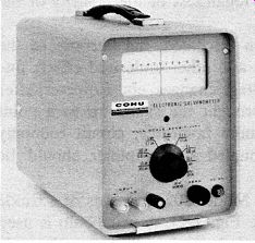
Fig. 7-8. Cohu Electronics Model 204AR electronic galvanometer.
The next instrument selected for discussion is manufactured by Cohu Electronics, Inc., San Diego, California, and is designated as their Model 204A. The instrument is a combination d-c null detector, microvolt ammeter, and an inverting d-c amplifier. It is functionally equivalent to suspension galvanometers, but the chopper-stabilized, all-transistor circuit provides many added features and numerous advantages over conventional moving-coil and electronic galvanometers. The instrument is insensitive to vibration, shock, micro-phonics, earth's magnetic field, and stray pickup. A photograph of the unit is shown in Fig. 7-8.
Theory of Operation
A block diagram of the Model 204A is shown in Fig. 7-9. The Model 204A consists of an input divider followed by a four-stage a-c amplifier incorporating an input chopper, a synchronous rectifier, and a three-stage d-c output amplifier.
The chopper converts the d-c input into a proportional a-c carrier signal which is amplified by the a-c amplifier. The output of the a-c amplifier is synchronously rectified, filtered, and applied to the d-c output amplifier.
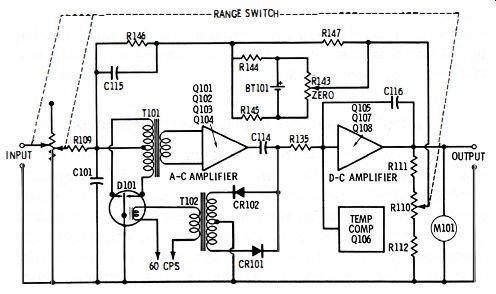
Fig. 7-9. Block diagram of Model 204AR.
Stability and constant input-impedance are maintained by using a large value (approximately 50 db) of inverse feedback. With this value of feedback, overall gain accuracy is determined, essentially by the accuracy of the feedback and input-divider networks, which consist of stable precision resistors. The range switch sets both these networks for the appropriate range. This control functions as an Ayrton shunt, which is usually an accessory for conventional galvanometers.
Input and Chopper Circuit---The input signal is fed through R109 to the center tap of the input transformer. R 109 sets the d-c gain, either direct or attenuated (depending on the position of the range switch), and forms (in conjunction with C101) a filter. This filter attenuates the 60- hz component that may be present on the signal (due either to leakage or stray fields). A-C Amplifier Circuit-The secondary of the input or chopper transformer feeds the first stage of a four-stage, transistorized, a-c amplifier (q101 through q104). The output of this amplifier is coupled to the d-c amplifier.
Rectifier Circuit---Diodes CR101 and CR102 are connected to form a half-wave bridge rectifier circuit and are supplied with a 60 hz signal phased to the chopper drive. These diodes rectify the output of the a-c amplifier, and the resultant d-c signals are applied to the input of the d-c amplifier.
DC Amplifier Circuit---The d-c amplifier consists of three transistorized amplification stages (0105, 0107, and 0108). Temperature compensation is provided by a fourth transistor (01 06), which is connected as a diode. The output of the d-c amplifier is applied to the meter and the output terminals.
Battery Feedback---Battery BT101, its associated resistors, and a potentiometer form a bridge which can insert a positive, negative, or zero voltage in series with the feedback resistor. This is effectively equivalent to the insertion of an input zero-adjusting voltage.