AMAZON multi-meters discounts AMAZON oscilloscope discounts
This section is devoted to typical integrating digital-meter circuits. While the basic operating principles of all integrating digital meters are the same, it was shown in Section 1 that the circuits used in the different meters vary considerably.
MODEL 510
The instrument selected for discussion is manufactured by Vidar Corporation, Mountain View, California, and it is designated as their Model 51 0. It is representative of the basic integrating meter principle in that it combines two instruments in one (a voltage-to-frequency converter and a frequency counter) to provide a direct-reading digital display of an input voltage integrated over the gate (sampling) time selected. A step attenuator provides six calibrated full-scale sensitivity settings from 10 millivolts to 1000 volts . Fixed gate times of 10 msec, 100 msec, and 1 second are available, or any desired gate time may be used from an external source. Counter sensitivity of 0. 1 to 100 volts rms up to 300 khz is available with both front and/ or rear inputs.
An internal precision ± 1-volt calibrating source is controlled from the front panel for both checking and calibrating the instrument.
The binary-coded decimal (bcd) output on the standard 510 is the 1-2-4-8 code (with "0" positive) and is available at a connector located on the rear panel. Bcd outputs are provided for five digits, decimal location in negative exponents of ten, and the measurement units of plus volts, minus volts, or frequency. This connector also supplies a readout command and accepts a readout hold signal. A photograph of the unit is shown in Fig. 6- 1.
Courtesy Vidar Corporation
Fig. 6-1. Vidar Corp. Model 510 integrating digital voltmeter.
Fig. 6-2.
Fig. 6-3.
Basic Theory of Operation
The overall theory of operation is best understood by referring to the block diagram of Fig. 6-2. Surrounding most of the instrument is an outer shield which is formed by the instrument sheet-metal exteriors (Fig. 6-3). Contained within the outer shield and enclosing the voltage-controlled oscillator (vco) of the Model 510 is a guard shield.
In operation the guard shield is connected to source ground. The effect of the guard shield is to prevent the flow of common-mode currents in the input circuit. (Common-mode signals are discussed in later sections.) Contained within the guard shield is an inner shield. The inner shield is connected to the common rail of the vco power supply and forms an electrostatic shield for internally generated a-c voltages.
Within the inner shield is the vco proper. Multiple-shielded transformers provide for the coupling of a-c power to the vco and coupling of the pulse train output to the counter section of the instrument, while maintaining the triple shielding.
Basic VCO Circuit---The vco consists of a preamplifier, a voltage to-frequency converter, and a regulated power supply. The preamplifier is shown in block diagram form in Fig. 6-4. The preamplifier consists of an error amplifier and a precision divider (step attenuator) and operates in either of two modes, potentiometric or operational. The error amplifier is a high-gain, chopper-stabilized, low-pass, inverting amplifier. The input (source) signal is applied between the error amplifier input and an adjustable tap on the precision divider, for the millivolt ranges, or the inner shield for the volt ranges. An amplified output signal-out of phase with the input signal-appears at the preamplifier output terminals.
In the potentiometric mode, where the millivolt ranges are used, a fraction of the output signal appears at the junction of the precision divider resistors (R1 and R2). This divided output signal is fed back in opposition to the input signal. Since the error amplifier has very high gain, the divided output signal must very nearly equal the input signal. This is true because any difference in magnitude between the two signals will cause a corrective change in the preamplifier output signal. Therefore, the voltage gain of the preamplifier is very nearly equal to the division ratio of the voltage divider (RI -R2), and since the input signal is opposed by an equal-amplitude, opposite-phase signal, the input current required is essentially zero. Thus the input resistance is very high.
In the operational mode, where the volt ranges are used, the function is the same as just described except that the opposing signal is a current to balance the one provided by the input signal. The high gain of the error amplifier in this case affords essentially a zero input impedance at the mode. The preamplifier therefore has an input resistance essentially equal to R 1 and a gain of the ratio of R2 to R1.
(A) Potentiometric. (B) Operational.
Fig. 6-4. Block diagram of Model 510.
Contained within the error amplifier is a nonlinear feedback network. This internal feedback becomes effective only when the input signal exceeds a predetermined limit. When this limit is exceeded, both the gain and input resistance of the error amplifier are greatly reduced, thus preventing further increases in either amplifier input or output voltages. The effect of the nonlinear feedback is to prevent overloading of the error amplifier by abnormal input signals. Within a few milliseconds following removal of the abnormal input the internal feedback drops out and normal preamplifier operation is restored.
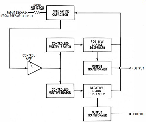
Fig. 6-5. Block diagram of voltage-to-frequency converter.
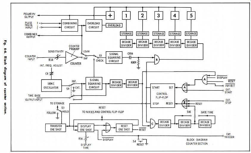
Fig. 6-6.
The output of the preamplifier is fed to the voltage-la-frequency converter (vfc) which is shown in block diagram form in Fig. 6-5.
A current proportional to the preamplifier output voltage is applied to an integrating capacitor. The nearly constant current applied to the capacitor causes the voltage across it to increase linearly with time (assuming that there is a positive output from the preamplifier). The output of the control amplifier, therefore, falls linearly (the control amplifier inverts) until the output becomes sufficiently negative to allow the controlled multivibrator (cmv) to produce one pulse. This pulse, applied to the positive charge dispenser, causes it to send a charge into the integrating capacitor. This in turn causes the voltage across the capacitor to decrease. This action results in the waveform across the capacitor having a sawtooth shape. The resultant decrease in output voltage from the amplifier causes the cmv to stop oscillating until the amplifier output voltage again reaches the triggering level.
The voltage appearing across the integrating capacitor is kept at a very low level because of the high gain of the control amplifier. To keep this voltage low the average current from the charge dispenser must be equal to Q (the charge quantum per cycle) and time, F (the number of charge quanta per second). Consequently, the frequency is precisely proportional to the input current. The accuracy of the system thus depends on maintaining the charge quantum precisely constant and keeping the voltage across the integrating capacitor very small, so that the input current is proportional to the input voltage.
If the input signal is of negative polarity, the integrating capacitor tends to charge in the negative direction. Consequently, the output of the control amplifier is positive, causing the negative rather than the positive charge dispenser to operate. The quantum charge from the negative charge dispenser is of opposite sign to that from the positive charge dispenser and therefore again tends to reduce the voltage appearing across the integrating capacitor. The pulse-train outputs are derived from the standard charge dispensers (scd) by means of transformers. Since only one scd operates at a time, there is only one pulse-train output at any given time.
The counter section is shown in block diagram form in Fig. 6-6.
This circuit consists basically of a combining circuit and a conventional 300- khz counter.
The combining circuit adds the pulse trains from both the positive and negative outputs of the vco and provides a single pulse train equal to the total . The vco output, which at any instant is providing the pulses, is sensed and used as a polarity indication. The combined output is discriminated in the overload circuit, the output of which controls a relay. When an overload exists, the relay is de-energized and the numerical Nixie display is extinguished and the word Overload appears in the lower-left corner of the display window. The combined output is also delivered to the counter input through the Gate Time switch when in the voltmeter sector. In the frequency sector the counter is connected to the output of a 300- khz bandwidth preamplifier, whose input is connected through an attenuator to the counter input.
To describe the general operation of the counter, let us consider that the Reset one-shot has been triggered in some manner. The reset pulse acts to (1) reset the display one-shot to its relaxed state, (2) reset the control flip-flop to the stop state through OR gate B, (3) clear all the controlled decade dividers to zero (this does not include the stored numbers), and (4) inhibit AND gate A. On completion of the reset pulse, if there is no external inhibit signal, the condition of AND gate A is totally determined by the output of the time base through the two uncontrolled decade dividers. Therefore, the first true pulse from the time base sets the control flip-flop to the start condition through OR gate A. This control condition opens AND gates B and C. The input signal which has been squared and differentiated is now counted through the five display decade dividers.
The time base pulses are also decade divided and the desired division is selected with the Gate Time switch. When a pulse appears at the output of the selected time-base decade divider, the control flip-flop is reset to the stop condition through OR gate B. This stop condition then initiates a trigger to both the transfer one-shot and the display one-shot. The transfer one-shot pulse, if the storage feature is being used, transfers the count accumulated in the display decade dividers to storage and the Nixie tubes. If the Follow state is used, the count is continuously carried on the display. The display one-shot, when set by the stop as previously discussed, starts the Display Time, which is controlled at the front panel and inhibits AND gate A. At the end of the display one-shot period the reset one shot is again triggered to start a repetition of the cycle. Note that at any time during the entire cycle described, a reset pulse will stop the cycle and restart it at the beginning. External controls can initiate certain conditions as shown in the block diagram.
Preamplifier Circuits
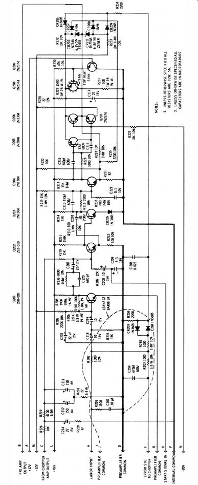
Fig. 6-8. Schematic of wide-band amplifier.
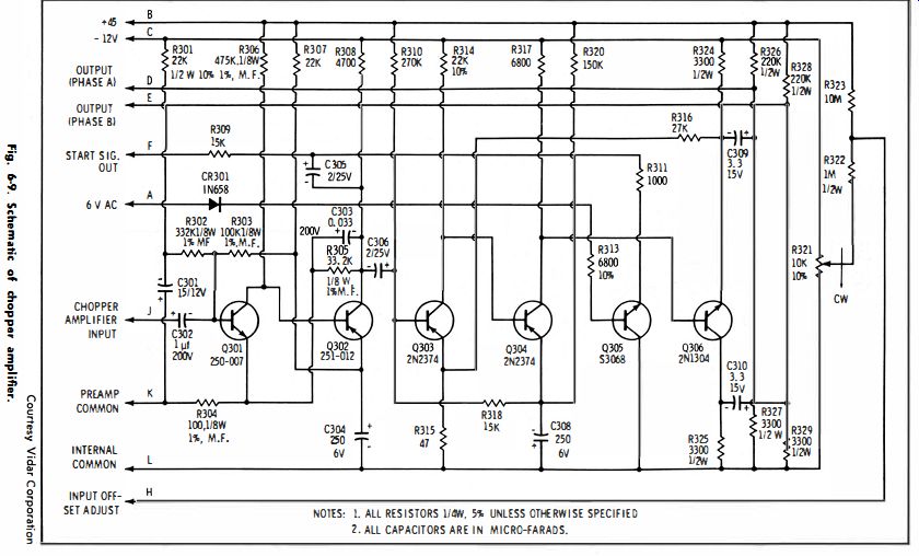
Fig. 6-9.
The overall operation of the preamplifier is best understood by reference to Figs . 6-7, 6-8, and 6-9 (Note: Fig. 6-7 is located on foldout page at end of guide ). As previously discussed, the preamplifier consists of an error amplifier and a precision divider (step attenuator). The error amplifier is a high-gain, chopper-stabilized, inverting d-c amplifier. Resistors R5 through R9 (Fig. 6-7) comprise the potentiometric precision divider, while R10, R11, R3, and R30 form the operational precision divider. The error amplifier is comprised of a wide-band amplifier (Fig. 6-8), a chopper amplifier (Fig. 6-9), and a chopper (Fig. 6-7). The precision attenuator has six positions, three for the potentiometric mode and three for the operational mode. The desired pre- amplifier gain is selected by the appropriate position of the three-pole switch (S I OA-C), which is maximum in the 10-millivolts (potentiometric) position and minimum in the 1000-volts (operational) position. The input to the preamplifier is applied between the terminals marked Signal Input Lo and Hi. The terminal marked Hi is connected to a tap on the precision divider in the potentiometric mode and to internal common in the operational mode. The terminal marked Lo is connected to the error amplifier through a combination of series resistors (R1, R2, and R4 ) and fuses (F2 and F3 ) in the potentiometric mode and to the input resistor (R 10) in the operational mode.
Resistors R1, R2, R4, R12, and R31 and capacitors C5 and C10 along with RC network R201-C201 provide high-frequency stabilization for the error amplifier.
Back-to-back diodes CR1 and CR2 in conjunction with fuses F2 and F3 provide protection for the error amplifier in case of heavy overload (in normal operation the diodes do not conduct). R202 limits the current applied to the error amplifier in case of heavy overload.
At the right end of R202, the error-amplifier input signal is split in terms of frequency.
The signal components from direct-current to about 15 hz are applied to the chopper amplifier via R203 and the input section of chopper K1. Alternating-current signal components are capacitively coupled (C218-R235-C219) to the first section of the wide-band amplifier, which amplifies signals in the range from about 15 hz to several hundred kilocycles.
The filter network of R203 and C204 prevents spikes associated with the action of the chopper from reaching the wide-band amplifier.
This amplifier is a cascade of three individual amplifier sections. The first amplifier section is a single-stage, inverting a-c amplifier. The first amplifier section, as do the second two sections, uses local negative feedback to ensure gain stability. The second amplifier section is a two-stage, noninverting d-c amplifier. The second amplifier section amplifies both the 15 hz to 100- khz output of the first amplifier section and the d-c to IS- hz output of the chopper amplifier. The third amplifier section has a relatively high output current capability. This capability is required to drive the parallel combination of the precision divider section, the vco section, and the overload circuit.
The chopper amplifier operates in conjunction with chopper K1 and consists of two individual amplifier sections. The first amplifier section is a two-stage, non inverting a-c amplifier. The first amplifier section, as does the second, uses local negative feedback to ensure gain stability. The second amplifier section is a three stage amplifier and phase inverter. The operation of the chopper-amplifier combination is best understood by imagining a small positive d-c voltage present at the input of the error amplifier (the small positive voltage might be due to a difference between the tap on the precision divider and the input signal voltage). The chopper is driven at line frequency (50 to 60 hz), and the chopper arms are energized in phase (as drawn, both arms are either up or down), The arm of the chopper input section (the input of the chopper amplifier) is therefore connected alternately between the small positive d-c voltage and a point which is near zero potential.
It should be noted that the upper contact of the chopper input section is not at zero potential, due to the d-c drop across R22. The voltage drop across R22 is adjusted by means of potentiometer R32 1 such that the potential between the chopper input-section contacts is zero with no input to the preamplifier.
The input to the chopper amplifier is therefore a series of line-rate pulses with peak-to-peak amplitude equal to the small positive d-c voltage (error voltage). These pulses are then amplified and phase inverted by the chopper amplifier. The chopper-amplifier output signals are designated as phase A and phase B. Phase A is in phase with the chopper-amplifier input, while phase B is 1800 from it.
Divider networks R326-R327 and R328-R329 bias the two output phases to an average positive level. The chopper-amplifier input and output waveforms are shown in Fig. 6-10.
Note that the waveforms are not symmetrical square waves. The chopper is constructed so that the contacts in the input section are closed for 45 percent of the line period, while the contacts on the output section are closed for 35 percent of the line period. Connection to the output section of the chopper is made in such a way that the chopped arm alternately samples 35 percent of line-period portions of the phase A and phase B outputs. The waveforms at the output section of the chopper are shown in Fig. 6-11 . Note that the chopper output, relative to the d-c bias level, is an average negative d-c voltage (the output of the chopper is inverted relative to the input).
(A) Input. (B) Output phase A. (C) Output phase B.
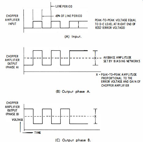
Fig. 6-10. Diagram of chopper waveforms.
The chopper-amplifier output is applied to a low-pass filter (resistors R226, R220, R2 19, R2 18, and capacitors C214, C211, C212). The smoothing action of the low-pass filter removes the a-c component of the chopper-amplifier output (the a-c component is due to noise in the chopper amplifier). The output of the low-pass filter is combined (via resistor R2 1O) with the output of the first amplifier section of the wide-band amplifier. Also combined at this point is the output of the start circuit (0305). The operation of the start circuit is as follows. 0305 functions as a synchronous rectifier by clamping to zero (common) potential alternate haf-cycles of the pulse waveform which appear at the output of the first amplifier section of the chopper amplifier. The base of 0305 is driven (via CR301 and R3 13) by a 6-volt a-c line rate signal. This same signal energizes chopper K1 . 0305 conducts during alternate half-cycles of the line-rate drive signal. The waveform at the junction of R309 and R3 11 is shown in Fig. 6- 12.
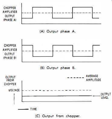
Fig. 6-11. Diagram of chopper output-section waveforms.
(C) Output from chopper. (A) Output phase A.
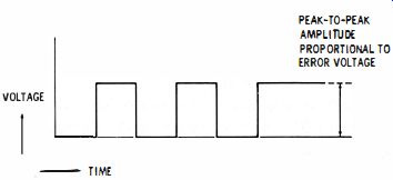
Fig. 6-12. Waveform at junction of R309 and R311.
This waveform is applied to low-pass filter (R309-C209). The d-c voltage across C209 is proportional to the chopper amplifier input voltage, while the a-c voltage across C209 is proportional to the change of chopper-amplifier input voltage. The start circuit makes use of the a-c signal across C209. This signal is summed (via C208-R209) with the filtered chopper-amplifier output and the output of the first amplifier section of the wide-band amplifier. The a-c signal across C209 anticipates a change of voltage at the filtered output of the chopper amplifier. A greater time is required to change the voltage at the output of the chopper amplifier. This is due to the relatively long time constant of the chopper-amplifier output filter, it is compounded by the saturation of the second amplifier section of the chopper amplifier. This occurs when the instrument is first turned on. The anticipating signal derived from the start circuit enables the error amplifier to reach a stable operating condition following the initial condition which exists when power is first applied to the instrument.
The combined outputs of the start circuit, the chopper-amplifier chopper combination and the first amplifier section of the wide-band amplifier, are amplified by the second and third (output) sections of the wide-band amplifier. The output stage of the wide-band amplifier consists of a complementary symmetrical emitter-follower connected between + 12 volts and -12 volts. It is desirable to restrict the preamplifier output range to a value slightly in excess of the normal operating range (+6.25 volts to -6.25 volts). Restriction of the preamplifier output range is accomplished by the overload circuit.
The effect of the restriction is to decrease the susceptibility of the error amplifier to overload from abnormal input signals.
Operation of the overload circuit is as follows. Current flows through zener diodes CR2 10 and CR211 via resistors R232 and R233, respectively (note that R232 and R233 are returned to + 12 volts and -12 volts, respectively, and that the junction of CR2 10 and CR211 is returned to the preamplifier output) . The voltage at the junctions of R233-CR2 11 and R232-CR2 10, therefore, differs from the preamplifier output voltage by the zener voltage (6.5 volts ±5 percent). The voltage at the junction of R233-CR2 11 is 6.S volts negative with respect to the preamplifier output, and the voltage at the junction of R232-CR2 10 is 6.5 volts positive with respect to the preamplifier output. Therefore, the voltage at the junction of R233 CR211 will be zero when the preamplifier output voltage is 6.S volts, and the voltage at the junction of R232-CR2 10 will be zero when the preamplifier output voltage is -6.5 volts.
Diodes CR206-CR207 (connected to the junction of R232-CR2 10) and CR202-CR209 (connected to the junction of R232-CR2 11 ) are connected to near zero (internal-common) potential points. Diodes CR20S and CR209, therefore, conduct when the potential at the junction of R233-CR211 is about zero. Similarly, CR206 arid CR207 conduct when the potential at the junction of R232-CR210 is about zero.
Note that since CR207 and CR20S are germanium diodes and CR206 and CR209 are silicon diodes, CR207 will conduct prior to CR206 and that CR20S will conduct prior to CR209. Therefore, R207 or CR208 will go into conduction when the preamplifier output reaches about plus or minus 6.S volts. When CR207 or CR20S go into conduction, R224 the wide-band amplifier output-stage feedback resistor) is shunted by R225, thereby reducing the wide-band amplifier gain, hence reducing the error-amplifier gain. A further increase in preamplifier output causes either CR206 or CR209 to conduct. When CR206 or CR209 conduct, overall feedback is applied around the error amplifier via divider network R234, R204, C206), back-to-back diodes CR203 and CR204, and resistor R238.
The effect of the overall feedback is to greatly reduce the input impedance of the error amplifier (the current fed back around the error amplifier opposes the input current). The greatly reduced input impedance tends to prevent a further rise in input voltage with consequent saturation of the error amplifier and subsequent prolonged recovery time.
The +12 volts necessary for operation of the wide-band amplifier output stage and the overload circuit is derived from the +45-volt supply by means of a shunt regulator (0208-0209). The + 12-volt output of the vco power supply provides the reference voltage for the +12-volt supply.
Several precautions are taken to enhance the performance of the preamplifier in terms of stability and noise. These include the use of high-accuracy resistors in the precision divider, the use of noise selected transistors in low-level stages, the use of shielded wiring in low-level stages, and a carefully worked-out wiring arrangement.
Voltage-to-Frequency Converter Circuits
The control amplifier (Fig. 6-13) amplifies the sawtooth waveform appearing across the integrating capacitor along with any d-c level appearing at this point. The output of the control amplifier drives the standard charge dispensers. The amplifier must have wide bandwidth in order to amplify the sawtooth waveform with good fidelity.
The amplifier must also have high gain and low input offset voltage in order to maintain the d-c voltage appearing across the integrating capacitor at nearly zero, thus making the input current accurately proportional to the input signal voltage.
The control amplifier consists of two cascaded differential amplifiers (Q40 1A-Q40 1B and 0403-0404) followed by an emitter follower (Q405). Q402 acts as a high-impedance load for 0404. The control amplifier input signal (the preamplifier output) is fed to the base of 040 1 via input resistor R403. Back-to-back diodes (CR40 1 and CR402) protect the control amplifier from excessive input voltages.
0401 base-to-ground voltage is set at zero by adjustment of the first differential-amplifier operating point. This adjustment is provided by voltage divider R4 1 3-R4 10 in the base circuit of 0402 (note that selected resistor R4 13 may be connected to either +45 volts or -12 volts.) A variable offset current derived from the +45-volt supply via potentiometer R23 (the zero calibrate control) and resistors R402 and R406. The offset current may be adjusted to give zero-frequency output from zero input to the meter. The control-amplifier output is taken from the emitter of 0405. The capacitor (C402) provides the amplifier with overall integrator-type feedback which aids in forming the sawtooth triggering waveform.
Fig. 6-13. Schematic of control amplifier.
Several precautions have been taken to reduce doc drift in the amplifier. The differential amplifiers both make use of low leakage silicon transistors. In addition, the input pair (040 1A-0401B) shares a common header and uses transistors which have been matched for emitter-base voltage tracking over the operating temperature range.
Positive Standard Charge Dispenser---The positive standard charge dispenser (sed) is driven by the output of the control amplifier and supplies the precision quanta of charge to the integrating capacitor.
The charge dispenser is made up of a controlled multivibrator (cmv), an emitter-follower amplifier, a switch transistor which drives the precision capacitor, switch diodes, and a constant-current source (Fig. 6-14).
Transistors 050 1 and 0502 comprise the cmv. The output of the cmv is amplified by emitter follower 0503 and is used to drive the switch transistor (q504). Consider the operation of the circuit when it is in the resting condition. In this condition, 0504 is turned on and saturated by base current supplied through R5 11 , making the collector voltage of q504 +45 volts. Some of the load on the collector of q504 is caused by the voltage divider (R516-R5 17). The voltage at the junction of these resistors is +6.3 volts. Therefore, CR505 is turned off, and the voltage at the junction of CR501 and CR502 is determined by the control-amplifier output voltage.
Transistor q502 is held off by the current from the 45-volt supply (R510, CR502, and R505). Since one half of the cmv is held off, the other transistor is on, but not saturated. The current through q501 is controlled by maintaining the base voltage at -2.9 volts by means of the voltage divider (R501-R502). Current in q501 is determined by the emitter voltage and R502. The cmv is thus held in a stable state for all voltages from the control amplifier which are more positive than the -2.7 volts on the emitter of 0502. In the operating condition, however, the output of the control amplifier becomes negative and will eventually become more negative than the voltage at the base of q502. When this occurs, q502 turns on, and the cmv is triggered.
The normal operation of the cmv then turns off q501 because of the rise in the collector voltage on q502 which is transmitted through C502. The collector voltage on 050 1 falls and causes q502 to stay on, regardless of the voltage at the output of the amplifier. The rise in voltage at the collector of q502 is also coupled to the emitter follower and then to the base of the switch transistor, q504. The switch transistor is thus turned off, and its collector voltage falls toward ground level. The fall in collector voltage makes the junction of R516 and R5 17 become negative, thereby turning on CR505 and turning off both CR501 and CR502. The influence of the control amplifier is removed from the cmv until the switch transistor is again turned on.
The switch transistor (q504) is turned on at the end of the pulse produced by the cmv.
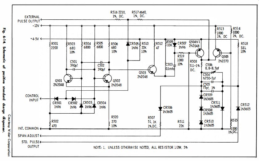
Fig. 6-14.
In normal operation the output of the control amplifier will have decreased below the triggering level in this length of time due to the standard charge dispenser will have sent a standard unit charge into the summing point. If this is true, the circuit will remain in the resting state until the sawtooth waveform at the output of the control amplifier again becomes sufficiently negative to trigger 0502. Consequently, in this mode of operation the cmv operates as a controlled multivibrator producing one pulse each time the output of the control amplifier becomes more negative than -2.7 volts. If the unit is overloaded by the application of a large positive signal, the output of the control amplifier will become more negative than -2.7 volts, and the multivibrator will operate as a free-running multivibrator. The cmv also "free-runs" when the instrument is first turned on and has not established its equilibrium condition.
As previously discussed the output of the cmv is amplified by the emitter follower (q503) and is then applied to the base of the switch transistor (qS04). This transistor is normally on when the standard charge dispenser is inoperative. In this case the precision capacitor (C504 in parallel with C505 and CS06) is charged to some positive value. The exact voltage is determined by the setting of R24 (the plus calibrate control). R24 sets the voltage applied to the catching diode (CR506). The effect of changing R24 is to adjust the positive voltage to which the precision capacitor charges.
The standard quantum of charge is generated by alternately connecting the precision capacitor to the positive voltage and then to ground as qS04 is turned on and off. The right end of the precision capacitor is connected to the two switch diodes (CRS 11 and CRS12). When the precision capacitor is connected to the positive voltage, the charging current is through CRS11 to ground. The time constant of the charging circuit is such that the capacitor becomes nearly fully charged. Thus a charge (Q = CE, where E is the positive voltage) is placed on the capacitor. Turning the switch transistor (OS04) off causes the left end of the precision capacitor to fall towards -12 volts, but the left end is caught at about ground potential by clamp diodes (CRS08, CRS09, and CRS 10). The discharge current of the precision capacitor is through the second switch diode (CRS I2) into the integrating capacitor (C401). q505 in conjunction with resistors (RS13, R514 and R515) acts as a constant-current sink, feeding the charge to the precision capacitor and thereby reducing the time required to discharge. The precision capacitor is completely discharged through this path. Therefore, the charge delivered to the integrating network is again equal to CEo To make the charge delivered precisely constant the precision capacitor must alternate between the same voltage limits during each cycle of operation. This is accomplished by making the upper limit of the voltage excursion the pre adjusted positive voltage and lower limit the diode clamp voltage. The precision capacitor is chosen to have a very small temperature coefficient. The residual coefficient is compensated by the negative temperature-coefficient capacitor (CS04). The exact amount of charge delivered per cycle can be adjusted by the trimming resistor (R24). Adjustment to compensate for component tolerances in the charge dispenser is accomplished by the trimmer capacitor (C506). R24 allows adjustment over a range of about ± 1 percent.
The pulse-train output of the unit is taken from the collector of q504 via the output transformer (T2). The transformer is loaded by R26.
Negative Standard Charge Dispenser--The negative and positive standard charge dispensers are similar in all respects except for input signal polarity and output charge polarity. In the negative scd (Fig. 6- 15), transistors q601 and q602 comprise the controlled multivibrator (cmv), q603 is the emitter-follower amplifier, q604 is the switch transistor, and q605 is the current source.
In the negative scd, the switch diodes are reversed and the cmv transistors are npn types. The cmv is triggered when the input from the control amplifier becomes more positive than the voltage across R603. The cmv provides the signal input to 0603 and the npn emitter follower which drives switch transistor q604. q604 is normally in the off condition. Therefore, in the resting condition the precision capacitor (C606 in parallel with C607 and C608) is discharged. Note that in the negative scd the polarities of the two switch diodes (CR611 and CR6 12) are reversed from those in the positive scd. Therefore, the sign of the charge delivered to the integrating capacitor is also reversed.
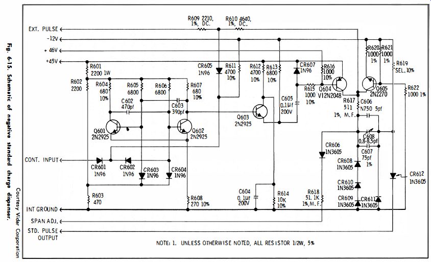
Fig. 6-15
The pulse-train output is taken from the collector of 0604 via the output transformer (T3). The transformer is loaded by R27.
vco Power Supply---The voltage-controlled oscillator (vco) power supply provides two regulated outputs, -12 and +45 volts, and one unregulated output of -22 volts. Operation of these circuits is typical for power supplies of this type. These circuits will not be discussed since they are not unique to an integrating digital voltmeter.
Pulse-Combining and Counter Circuits---A simplified composite schematic of the counter section is shown in Fig. 6- 16 (Note: Fig. 6-16 is located on foldout page at end of guide) . This entire section is contained on six basic types of printed-circuit boards. They are the input processing circuits (PC801), the counter control circuits (PC70 1), the time-base source (PC1001), the decade dividers (PC1101-PC1 105), the decade displays (PC901-PC905), and logic conversion circuits (PC1201-PC1301 ). The manually switched logic and circuit interconnections are also shown in schematic form on this drawing. The decimal-point location logic is done with switches S8A, S8B, S8C, and S6B. The unit's logic is performed by switches, S8D and S6D. Negative-true logic is employed throughout the counter section with "zero" equal to or greater than -1.2 volts and "one" equal to or less than -9.5 volts.
Pulse-Combining and Polarity Circuits---These circuits are contained on the input board (PC80 1 in Fig. 6-1 6). The positive pulse train output from the voltage-to-frequency converter is amplified and inverted by Q801, then differentiated by C804 and R8 14, while the negative pulse-train output is directly differentiated by C802 and R8 13. The positive swing of either pulse train will therefore trigger the one-shot comprised of Q806 and Q807. The secondaries of the transformer load (T801) of Q807 are cascaded and applied to the counter input. The center winding of T801 is loaded by R20 and available as the combined output pulse train. The negative swing of the positive and negative differentiated pulse trains is applied to the bistable multivibrator composed of Q804 and Q805 in such a manner as to set it to one state or the other, depending on which output of the voltage-to-frequency converter is producing pulses.
The high voltage is applied to the plus or minus Nixie tube through the Gate Time switch (S6C) in the voltmeter sector only and through the current-limiting resistor (R812) to provide a continuous minus sign display. When a pulse appears at the positive output of the converter, Q804 is turned on and the plus sign lights through the driver transistor (Q809). A logic level is also provided from this flip-flop for polarity indication, a "one" signifying positive voltage input.
Overload Circuit---The output pulses of the combining circuit are constant in duration and therefore may be used in a standard charge dispenser much the same as previously described. In this case the average current and supplied current is integrated by a capacitor and the differential current is sensed. When this differential current which is proportional to the pulse repetition rate, exceeds a predetermined value, a relay is deactivated which illuminates the overload indicator, extinguishes the display, and provides a contact break from ground on pin 45 of 110. The overload detection circuit is contained on the control board (PC701) and is shown at the lower left of Fig. 6-16. The relay and indicator are mounted on the bottom of the decimal point assembly.
The combined output at J7 is applied to the base of Q713 which is normally biased off by the low source impedance of T80 1 and the difference between the base-emitter drop of the silicon transistor (Q713) and the forward drop of the germanium diode (CR710). When a positive pulse occurs both Q713 and Q7 14 are turned <;>0 for the duration of the pulse, taking the collector of q714 to the + 15-volt level and charging capacitor C701 through R 719 and CR no. At the end of the input pulse, 07 13 and 07 14 turn off again, and C701 is discharged through CRn1, R7 19, and R7 12. The left end of capacitor C701 is caught at ground potential by diode CR719. The original charge on the capacitor C70 1 was C x 15 volts, since the drop in the switch transistor is negligible. The charge delivered to the integrating capacitor (Cn2) is thus the initial charge minus the final charge which is very nearly zero because the choice of the pulse length is sufficient to allow complete discharge of C701.
Each pulse transfers the same quanta of charge. Therefore, the average current out of the integrating capacitor is proportional to the pulse repetition rate. Resistors R no and R n2 provide current to the circuit, and q715 is turned on as long as insufficient current is being removed from the circuit by the charge dispenser (as a result of the pulse rate being too low). As the pulse rate increases, a point (adjustable by R nO) is reached at which insufficient current is available to maintain conduction of q715, and it turns off. 07 16 provides temperature compensation and allows q715 to be a non-saturating switch.
When q715 turns off, q717 also is turned off, and the relay ( K2) is thereby de-energized. One contact of K2 is available as a break in continuity on the Bcd Output connector, no. The other opens the short circuit across the overload indicator neon lamps and disconnects the high voltage from the Nixie numerical display. The full high voltage applied across the series overload neons causes their breakdown, and the sustained breakdown voltage of both neons in series is large enough to hold the Nixie high-voltage line below their breakdown voltage level. Resistor R40 limits the current through the overload neons.
Counter Preamplifier---The counter input is applied through C6 and R13 to the arm of the potentiometer (R14). C7 produces high frequency boost to offset cable losses due to the high impedance of the attenuator. Transistors 08 10, 08 11 , and 08 14 located on the input board (PC801) comprise a 300- khz bandwidth, high-gain amplifier with voltage feedback across R830. The high-frequency roll-off is accomplished by the capacitor (C814) and the low-frequency cut-off by C809. Emitter follower 08 14 reduces loading of q811 to maintain high open-loop gain and also provides low output impedance to reduce loading effects.
Time-Base Oscillator---The time oscillator and Schmitt trigger are located on the source board (PC1001). The oscillator is crystal con-trolled and is a switching-type network consists of transistors (Q1004 and Q1005) and the crystal (X1001 ). The crystal can be considered as a series-tuned circuit, driven from a current source and resonant at 100 khz. Due to the low input impedance of Q1004 nearly all the current through the crystal must flow into the base of Q1004.
The regenerative action of the emitter coupling requires the collector of QI005 to be in phase with the base of Q1004. Therefore, the series resonant circuit allows sustained oscillation only at the resonant frequency when zero phase shift exists. The trimmer capacitor (C8) allows a small amount of phase shift to be introduced at the base of Q1O04 and thereby "pull" at the frequency of oscillation slightly (about ±3 hz). The output of the oscillator is capacitively coupled through C1005 and R29 to switch S9 where it is either grounded when an external time base is used or applied to the base of the amplifier transistor (Q1001). The collector of Q1001 is then coupled to a conventional Schmitt trigger circuit composed of Q1002 and Q1003. The collector of Q 1 002 provides a signal at time base used in the counter Check mode. The output of the squaring circuit goes through R1021 and C9 to S9 where it is connected through R21 to the output connector J9 when the internal time base is used. When S9 is in the external position, J9 becomes an input which is applied through R2 1 and C1001 to the amplifier Q1001 in the same manner as the oscillator output previously described. The Schmitt trigger output also goes to the first decinary.
Decinary---Five identical decade dividers are cascaded from the time base to provide output frequencies of 10 khz, 1 khz, 100 hz, 10 hz, and 1 hz. The lower three frequencies are used to establish the three fixed gate times. Gating of the time base is done at 1 khz.
The three gate-time decinaries are reset each count to ensure accurate timing.
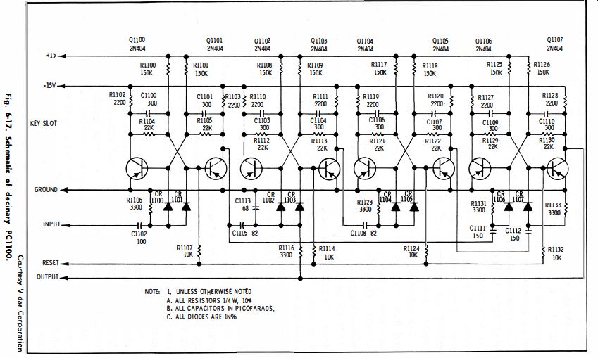
Fig. 6-17.
Each decinary consists of four binaries in series. A typical decinary schematic is shown in Fig. 6-17. Feedback is so arranged as to produce a bcd weighting of 1-2-4-8 for each successive binary. The carry line thereby produces one pulse for each ten applied to the input.
Display Decades---The five display decades each perform three basic functions: they divide the counted pulses by ten and carry every tenth pulse to the next decade in the same fashion as the decinaries; they store the accumulated count when a transfer command is received; and they convert the bcd output to ten-line code and drive the Nixie tube with the resultant information. Each of the display boards are identical, except for the first binary of the unit's decade which is of higher speed to ensure accurate counting through 300- khz input pulses. A typical display-decade circuit is shown in Fig. 6-18.
The decade-divider portion of the circuit functions identically to the decinary previously discussed (the carry line delivers every tenth pulse to the next display-decade input). Each binary is connected to the reset line, and each binary output is coupled through gating networks (R998, R996, R997, and R999) and is a typical storage binary.
The output of each storage binary is connected to the bcd ten-line decoding matrix (R934 through R963) and the bcd output through resistors R964-R967 to connector 110. When the transfer line is grounded the levels of the decade divider binaries are transferred continuously to the storage binaries. When the transfer line is held positive the resistor ratios prohibit the information transfer from decade divider to the storage binaries. The Nixie drivers q908 through q917 are directly coupled to the resistor logic matrix and the collector of each to the appropriate numerical indication in the Nixie tube.
Counter-Control and Gating Circuitry--The output of either the combining circuit or the counter preamplifier is selected by the Gate Time switch (S6F) and then either that signal or the 100-khz Check signal is selected by S5 and applied to the input Schmitt trigger composed of q812 and q813 (Fig. 6-16). Capacitor C816 and resistor R809 differentiate the squared waveform at the collector of q813 when the base of 0803 is held negative by the start signal from the control flip-flop. The negative-going pulses are then amplified by saturating amplifier q802 and delivered to the input of the unit's decade display divider.
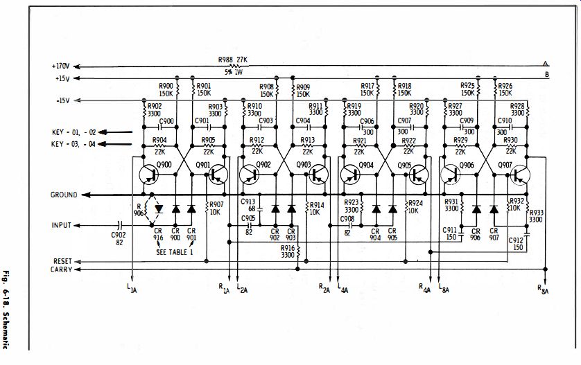
Fig. 6-18
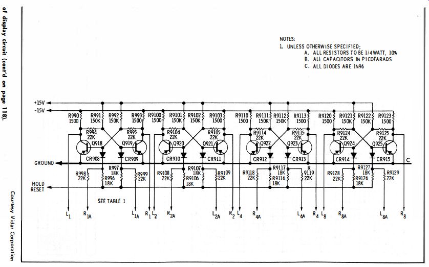
Fig. 6-18. Schematic of display circuit.
The reset one-shot may be triggered from three sources : (1) closure of Reset switch S4, (2) a positive-level shift from an external source through Ext Trig (111 ), or (3) by termination of the display time (transistor q706 turning on). The negative reset pulse, of about 180 microsecond duration, is current amplified through transistor 0709 and delivered to the reset line. Decinaries PC1103 through PC1105 and all decade dividers in the display decades are set to the zero state by the reset line. The reset pulse is applied to the control flip-flop to reset it in the stop mode (q701 on and q702 off). Note that only if q702 is on at the time the reset pulse occurs will a transfer pulse be generated by action of the reset one-shot. The positive reset pulse is used to terminate the display and as one of the control AND gate signals.
Consider now the condition of the control AND gate at the base of the emitter follower (q703). The beginning of the reset pulse has turned off 0704 in the display one-shot (assume that there is no external inhibit signal) ; at the completion of the reset pulse the base of q703 will have the output of the 1- khz decinary applied to it (CR 714, CR 706, CR 705, and CR 708 all are back -biased). The first positive swing of q703 base will set the control flip-flop to the start condition (q70 1 off). The start signal applies the necessary negative voltage to the base of q803 to "open" the input gate and also allows the time-base gate to follow the output of the 1- khz decinary. Therefore, the pulse which started the control flip-flop is also the first pulse counted in the 100- hz time-base decade dividers. Depending on the Gate Time setting, either 10, 100, or 1000 milliseconds after the start, a positive stop pulse is applied to the reset side of the control flip-flop. The stop condition of the control flip-flop (q702 off and q701 on) terminates the count by causing both the input and the time-base gates to "close," as well as triggering the transfer and display one-shots. The transfer one-shot negative pulse is alternating-current coupled through q712 to effect a level shift and produce about a 33-microsecond negative pulse referenced to the positive supply on the transfer line.
There are actually three modes of operation of the display one shot : first as a variable-duration pulse generator; second, as a bistable flip-flop; and third, as a fixed bias to one state.
In the pulse-generated mode, the Infinite switch (S2) and Gate Time switch (S6E) connect the negative supply to the junction of R18 and R17. The display one-shot duration is then controlled by the RC time constant of R16 plus R18 and C710. Emitter follower q705 reduces effect of collector load on the time constant and provides a fast recharge time constant nearly independent of the discharge time setting of R16. Diode CR3 is back-biased and made of silicon, thereby offering very little shunt resistance to the timing resistance of the timing resistors. This period is variable from about 60 milliseconds to about eight seconds. When the Infinite switch (S2) is pulled the junction of R17 and R18 is connected to the anode of CR175 while CR3 is forward-biased. Therefore, R 725 is placed in parallel with C710, and the flip-flop becomes bistable. When any of the external or manual functions are in use, S6E opens and CR3 becomes forward-biased, clamping the base of Q706 to the positive supply through R17.
Under this condition q706 is kept from conducting, and the control AND gate is clamped to chassis ground through CR 706, q704, and CR716.
In fixed gate time operation the negative trigger pulse from the "stop" signal of the control flip-flop is applied through CR 717 to the base of Q704, turning it on and thereby starting the display one-shot pulse period. With Q704 on the control AND gate is biased "closed" until the termination of the display time.
The reset one-shot is triggered by this termination from the collector of Q706, and again the control AND gate is biased "closed" through CR708 and CR705, which completes the entire control cycle. The two series diodes are used to match the various output levels at the gate and thereby remove the possibility of false triggering.
External and Manual Modes
In the External and Manual modes the display one-shot is biased to a state which will hold the control AND gate "closed." The control flip-flop then can only be triggered by signals through CR 703 to start the count, and R 704 to stop the count. For external control External Start (1 12) is used to start, and External Stop (J 13) is used to stop the control flip-flop. The external signal may be either a closure to ground or a three-volt positive step. The manual start signal is taken from the Gate Time switch (S6B) and the stop signal from S6A.
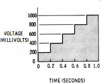
Fig. 6-19. Graph of the integral of a nonrepetitive waveform.
USING AN INTEGRATED DIGITAL VOLTMETER
The integrated digital voltmeter has certain advantages over the non integrating type. However, the principal advantage is its ability to obtain the integral of a voltage over a given time interval . For example, assume that it is desired to obtain the integral of the nonrepetitive waveform shown in Fig. 6-19.
The voltage-time integral is equal to the area enclosed by the waveform. The area may be obtained by considering the waveform as being composed of a series of 0.2-second bars of increasing height (voltage ); the total area consists of the sum of the areas of the individual bars. The area (A) is then A = (200 mv x 0.2 sec) + (400 mv x 0.2 sec) + (600 mv X 0.2 sec) + (800 mv X 0.2 sec) + (1000 mv X 0.2 sec) = 600 mv-second
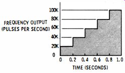
Fig. 6-20. Graph showing output as (PULSES PER SECOND) 60K integral in voltage
to frequency 40K conversion.
If the waveform of the example were applied to an integrated digital voltmeter such as the Model 510 (set to the 1000-mv range) the voltage-to-frequency converter output would be as shown in Fig. 6-20. When the frequency output is applied to the counter portion and if it is gated "on" at the beginning of the waveform and "off" at the end of the waveform, the reading would indicate the total number of pulses emitted by the converter during the one-second gating period.
This number can be derived by considering the frequency output of the converter as consisting of a series of 0.2-second bars of increasing height (frequency), the total number of pulses consisting of the sum of the number of pulses emitted during each 0.2-second period. The total number of pulses (N) is:
N = (20,000 pps X 0.2 sec) + (40,000 pps X 0.2 sec) + (60,000 pps X 0.2 sec) + (80,000 X 0.2 sec) + (100,000 x 0.2 sec) = 4000 + 8000 + 12,000 + 16,000 + 20,000 = 60,000
Observe that not only is N (the reading) an accurate indication of the area under the waveform (the integral), but that the means by which N is derived is exactly analogous to the means by which the integral was originally derived (by adding a number of small areas). To obtain the units of millivolt-seconds from the reading a factor must be applied to N as follows:
full-scale millivolts (range)
10^5 (full-scale pulses per second)
In the example given, we have N range
= 60 000 1000 X 10^5
' lOG
= 600 millivolt-seconds