AMAZON multi-meters discounts AMAZON oscilloscope discounts
The first practical semiconductor diode was the erratic crystal detector of the early 1900's. Although that device was superior to the coherer and magnetic detector which it succeeded, it eventually was supplanted, except in experimental equipment and toys, by the more sensitive and stable vacuum tube. The modern diode was developed in the 1940's as an answer to the demand for a radar detector free from the high-frequency limitations of the conventional vacuum tube. Thus, the diode has been present, off and on, throughout most of the history of radio communications.
In communications the modern diode does the same basic job of signal demodulation as the early crystal detector, but with greatly increased efficiency and reliability and no need for adjustment. It also does more; in radio it simplifies FM detector circuits, provides automatic amplitude and noise limiting and frequency control, and in television it does all of those jobs plus providing DC restoration, pulse separation, and sync clipping. And these are only a few of its functions in communications. This section describes typical receiver applications.
BASIC CRYSTAL RECEIVER
The crystal set is still the simplest and the only true emergency radio receiver, since its circuit is uncomplicated and its operation requires no battery or other local power supply. In this set the diode demodulates the amplitude-modulated RF signal and delivers AF power to the earphones. The diode does not amplify; consequently, it cannot boost the received signal. (In fact, since the diode is not 1001)"0 efficient in its operation, it delivers an output signal which is somewhat less than that which it receives.) Good crystal-set design attempts, through impedance matching and a high-Q tuned circuit, to transfer the maximum signal from the antenna to the diode and the maximum signal from the diode to the earphones of the receiver.
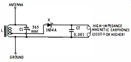
Fig. 1-1. Basic crystal receiver.
Fig. 1-1 shows the basic circuit. Here, the tuned circuit is composed of a transistor-type ferrite, loop antenna (L), and a 365-mmf variable capacitor (C1). The tuning range is 540 1,600 khz. The 1N34A germanium diode (X) is connected to the tap on the antenna coil for matching the low impedance of the diode. This prevents broad tuning, which would result from loading effect if the diode were connected across the entire coil. C2 is an RF bypass capacitor. The DC resistance of the magnetic earphones must be 2,000 ohms or higher. Do not attempt to use crystal earphones in this circuit. If the earphones are replaced with a 2,000-ohm, 1/2-watt resistor, the output of the circuit may be used to drive an audio amplifier.
In weak-signal areas the circuit works best with a good outside antenna and ground. Often the antenna may be a short piece of wire inside the building, or a window screen or bedspring. In medium- and strong-signal areas, no external antenna or ground will be needed as antenna coil L picks up sufficient signal when it is oriented correctly with respect to the broadcast station.
BANDPASS CRYSTAL RECEIVER
The broad tuning which is characteristic of many crystal sets is eliminated by the selective, high-fidelity, bandpass circuit shown in Fig. 1-2. This circuit uses the same bandpass filter type of tuner employed in some tube-type high-fidelity AM receivers. But in the crystal circuit, the connections to one RF transformer (T3) have been interchanged for better impedance matching to the IN 48S germanium diode detector (X) .
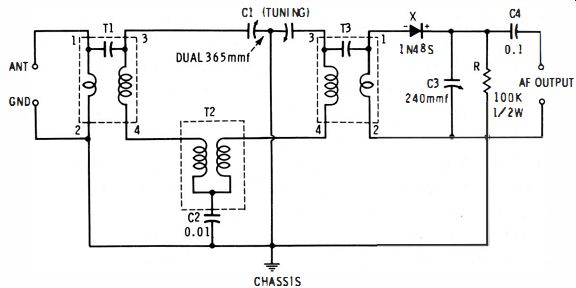
Fig. 1-2. Bandpass crystal receiver.
The circuit is tunable from 540 to 1,750 khz by means of the dual 365-mmf variable capacitor, C1. Transformers T1 and T3 are shielded antenna stage RF coils (Miller No. 242-A) ; T2 is a shielded negative mutual coupling coil (Miller No. EL-56) . The audio output of this circuit may be applied directly to crystal or magnetic earphones or to an audio amplifier.
POCKET RECEIVER
Use of miniature components can keep a receiver using the circuit in Fig. 1-3 small enough to fit into a shirt pocket. The antenna may be a length of thin, flexible wire stitched or clipped to the clothing. Such a receiver may be employed for broadcast listening or for actor cueing and personal paging from a nearby transmitter.
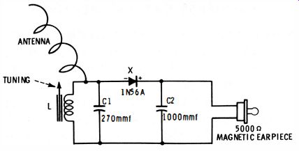
Fig. 1-3. Pocket receiver.
The tuner is composed of a 270-mmf silvered mica capacitor (C1) and slug-tuned ferrite loopstick antenna (L) . When L has an inductance variation range of 35-300 microhenries (Miller No. 2002) the circuit may be tuned between 550 and 1,600 khz with C1 equal to 270 mmf. Tuning is accomplished simply by adjusting the slug screw of loopstick L. The 1N56A germanium diode (X) drives a 5,000-ohm magnetic earplug which is bypassed for RF by capacitor C2.
If operation in the citizens' band is desired, L may be changed to a slug-tuned variable inductor having the range 1.5-3.2 microhenries (Miller No. 4404) and C1 to a 10-mmf silvered mica capacitor.
If the earphone volume is insufficient, a 1- or 2-stage subminiature transistorized AF amplifier may be added to the receiver.
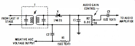
Fig. 1-4. Second detector.
SECOND DETECTOR IN AM SUPERHET
This is a common use of the diode in multistage radio receivers of both tube and transistor types. Fig. 1-4 shows a typical circuit in which a 1N63S germanium diode (X) acts both as a second detector and AGC rectifier.
In a transistor-type receiver, the secondary of IF transformer T will be the low-impedance winding ; C2 and C3 will be 1 to 10 mfd ; and R1, 3,300 ohms. In a tube-type receiver, T must be a half-wave detector-type IF transformer; C2, 10 mfd; C3, 0.1 mfd ; and R1, 5,000 to 50,000 ohms depending on the type of tubes to be controlled by the AGC voltage.
In addition to being small, without filaments, and free from heat, microphonics, and internal hum, the diode second detector provides lower dynamic impedance than the equivalent tube-type detector.
NOISE LIMITER IN AM SUPERHET
Fig. 1-5 shows a noise limiter (silencer) combined with a diode second detector and having automatic threshold control.

Fig. 1-5. Combined second detector and noise limiter.
In this arrangement, the 1N63S germanium diode (X1) acts as a conventional second detector-AGC rectifier. It also supplies a variable DC bias voltage, proportional to the IF signal, to the two 1N300 silicon junction noise-limiting diodes (X2 and X3) ; this is the automatic threshold voltage.
Normally, the AF output of the second detector is transmitted by the limiter network (C2-C3-X2-X3-R2-R3-R4 ) to the audio amplifier through coupling capacitor C4, with a small amount of attenuation by the circuit. But when noise is present on the signal, either X2 or X3 effectively short-circuits the noise pulse to ground-a positive noise pulse forward-biases X3 momentarily, causing this diode to conduct heavily and limit the AF amplitude; a negative noise pulse forward-biases X2 and produces the same limiting effect.
Silicon junction diodes are used for X2 and X3 because of their extremely high reverse resistance and ability to operate with high resistances R2 and R4. A germanium diode is satisfactory for the second detector (X1) .
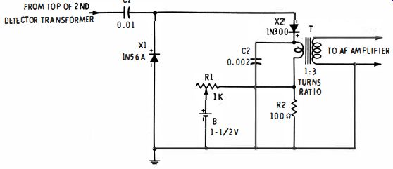
Fig. 1-6. Simple squelch circuit.
SQUELCH CIRCUIT
A simple squelch circuit for quieting a receiver between transmissions is shown in Fig. 1-6. Here, a lN56A germanium diode is connected as a shunt detector, through DC-blocking capacitor C1, to the secondary of the second detector transformer in the receiver. This diode delivers AF output corresponding to the modulation envelope of the received AM signal, and DC output which is proportional to the average carrier amplitude of the signal. This combined output is presented to gate diode X2.
The threshold of the gate circuit may be set at will by adjustment of rheostat R1 so that only signals of desired strength can pass through to the audio amplifier of the receiver. Weaker signals are held back ; hence, squelch action is obtained. The means for accomplishing this performance is the adjustable positive DC bias applied to diode X2. The bias voltage, adjustable from zero to 1.5 volts, is obtained from battery B through voltage-divider network R1-R2. This voltage reverse biases X2, and since this diode is a silicon unit, its leakage current is essentially zero. The positive DC component (carrier intensity) of the signal from X1 must exceed the positive threshold voltage before X2 will conduct and pass the AF signal through transformer T; as long as the signal amplitude is sufficiently below the threshold, no signal will pass through.
While a battery (B) is shown in Fig. 1-6, the DC source might also be the power supply of the receiver if the resistance of R1 is increased proportionately. Maximum threshold values other than 1.5 volts may be obtained by proper selection of input DC voltage and resistance of R1 and R2.
Transformer T may be any convenient interstage audio coupling transformer having an input-to-output turns ratio of 1 :2 or 1 :3. Capacitor C2 is an RF bypass.
FM DISCRIMINATOR
Fig. 1-7 shows a discriminator of the Foster-Seeley type for FM detection. Although this circuit is not critical in assembly or operation, its quality is enhanced by matching germanium diodes X1 and X2 and resistors R1 and R2. The specified 1N35S unit is composed of two matched 1N34AS miniature germanium diodes mounted on a single base. Resistors R1 and R2 should be matched within 170. Resistor R3 and capacitor C3 form a de-emphasis network of the conventional type.
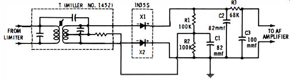
Fig. 1-7. FM discriminator.
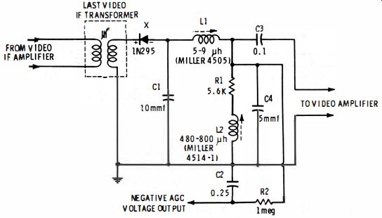
Fig. 1-9. Video detector.
FM RATIO DETECTOR
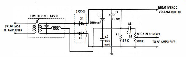
Fig. 1-8. FM ratio detector.
Another FM detector is shown in Fig. 1-8. The ratio detector, unlike the discriminator described in the preceding section, requires no limiter-an advantage when receiver layout must be simple and economical. This circuit delivers a negative AGC voltage, as well as AF output.
As in the discriminator, quality is improved by matching germanium diodes X1 and X2. The specified lN35S unit is composed of two matched lN34AS miniature diodes mounted on a single base. If the matched unit is not used, the individual diodes should be chosen to have forward conduction curves as nearly identical as possible. The gain control potentiometer (R2) may be the regular audio gain control of the receiver.
TV VIDEO DETECTOR
Fig. 1-9 shows a video detector for TV receivers and wide-range instruments. It takes advantage of the low shunting capacitance and low dynamic impedance of the 1N295 germanium video-detector diode.
The series-peaking coil (L1 ) and shunt-peaking coil (L2) are slug-tuned miniature inductors which may be set exactly for the desired pass band as viewed with an oscilloscope. For 4.5-mc bandwidth, L1 (Miller No. 4505 ) should be set to approximately 8 microhenries, and L2 (Miller No. 4514-1 ) to approximately 600 microhenries. Negative AGC voltage is supplied through filter C2-R2. Capacitors C1 and C4 are silvered mica.
DC RESTORER
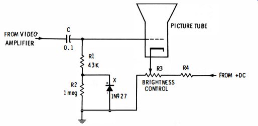
Fig. 1-10. DC restorer.
Both AC and DC information are present in the output of a TV video amplifier, but the DC component is lost when the signal is capacitively-coupled to the picture tube, as through C in Fig. 1-10. When this happens, the picture tube does not receive the average brightness information provided by the video signal, and the brightness control of the receiver does not completely compensate for this loss.
The DC component may be restored, however, through signal rectification by a germanium diode (X in Fig. 1-10) shunted across a part (R2) of the picture-tube grid resistor.
X is a 1N927 germanium DC-restorer diode.
DAMPER
The Q of magnetic deflection coils in TV and radar receivers is high enough for ringing to be produced by the sawtooth deflection currents. A damping resistor shunted across the coil will suppress this effect, but the resistor also robs the coil of current. A reverse-connected silicon diode in series with the resistor (X in Fig 1-11) will pass virtually no static current, since it is reverse-biased by the DC power supply ; but it will be forward-biased by the back voltage generated by the collapsing magnetic field at the end of the sawtooth sweep, and thus will switch the energy through resistor R in which it will be dissipated to prevent ringing.
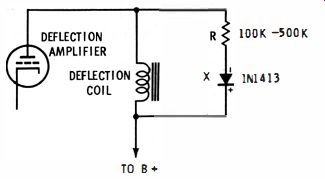
Fig. 1-11. Damper.
The specified 1N1413 silicon diode has a peak-reverse rating of 2,400 volts. At this voltage its reverse-leakage current is only 1 microampere. The value of resistor R will be between 100 and 500 kilohms and must be selected with respect to DC voltage, peak sawtooth voltage, and deflection-coil inductance in a particular circuit.
CLAMPING CIRCUITS
A diode clamp, like a DC restorer, is used to set or reestablish a DC reference potential in an AC circuit. Thus, either peak of an AC wave may be held to zero or to a selected amplitude, either positive or negative.
Fig. 1-12 shows a typical input wave which oscillates about the zero axis, and the corresponding output wave delivered by each of four clamping circuits. These are the simplest possible circuits, in which a clamping diode (X) shunts a conventional resistance-capacitance coupling circuit (RC). In 1-12A, the reference is clamped at zero, and the output signal swings between zero and a positive maximum amplitude determined by the peak input amplitude and rectification by the diode. Action of 1-12B is similar, except that the diode is reversed and the output swings between zero and a negative maximum amplitude. The circuits in Figs. 1-12C and D pro-vide, instead of zero, a reference level corresponding to a desired positive (+ E) or negative (-E) amplitude. The DC reference voltage is obtained from a battery, as shown, or from a power supply and voltage divider. In Fig. 1-12C, the output is positive-going and swings between the positive reference value (+ E) and a maximum amplitude determined by the input amplitude. In Fig. 1-12D, the output is negative-going and swings between the negative reference value (-E) and a maximum amplitude which is determined by the amplitude of the input signal.
(A) Zero reference, positive clamping.
(B) Zero reference, negative clamping.
(C) Positive reference, positive clamping.
(D) Negative reference, negative clamping.
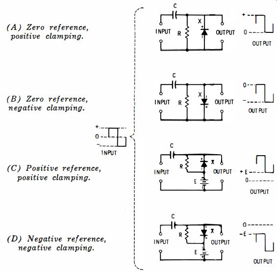
Fig. 1-12. Clamping circuits.
Diodes of all types may be used in clamping circuits ; however, they must be rated to withstand safely the combined applied AC and DC voltages. The R and C values in the coupling network must be chosen in the usual manner for optimum time constant at the desired operating frequency.
SYNC SEPARATOR (SYNC CLIPPER)
Diode-type sync separators are not often found in present day regular production TV receivers. However, this simple device will be preferred to the triode type in some transistorized TV circuits and in home-designed receivers in which complexity and size must be minimized.
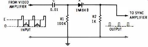
Fig. 1-13. Sync separator.
Fig. 1-13 shows one type of diode sync separator. This is essentially a shunt-diode rectifier with an additional resistor (R2) in series with the diode. The output signal is taken across R2. In this arrangement, the positive-going video signal, which contains picture information, sync, and blanking pulses, is applied to the circuit through coupling capacitor C. Diode rectified current develops a DC voltage across R1 (top negative, bottom positive ) and this voltage charges C. This capacitor remains charged at this level, equal to input signal E, because of the time constant CR1. The diode is biased to cutoff and the output is zero. The sync pulses drive the diode positive into forward conduction and produce corresponding output pulses which are delivered to the sync amplifier.
A 1N484B very low-leakage germanium diode (X) is used in this circuit. Capacitance C and resistances R1 and R2 may require some adjustment in individual circuits.
HORIZONTAL PHASE DETECTOR
Fig. 1-14 shows a phase detector for horizontal AFC in a TV receiver (in this case, the arrangement used in Philco Model TV7L40, but typical of the application). Since the frequency limit is not high, the wide-band characteristics of germanium and silicon are not needed. Consequently, a 6GD-1 dual selenium diode ( X1 and X2 ) may be used in this application.
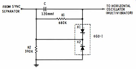
Fig. 1-14. Horizontal phase detector.
FM DYNAMIC LIMITER
A simple subcircuit composed of a capacitor, resistor, and high-conductance diode may be connected in parallel with the primary winding of an FM discriminator (or ratio detector) transformer to provide dynamic limiting action. (Fig. 1-15 shows the arrangement. ) In this circuit, T is the regular discriminator transformer.
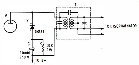
Fig. 1-15. FM dynamic limiter.
Here, a portion of the plate current of the last IF tube (V) flows through resistor R and the 1N281 high-conductance germanium diode (X) in series. This develops a diode self-bias voltage across resistor R. The high capacitance of C tends to maintain this voltage. The biased diode acts as a simple limiter or peak clipper, tending to maintain the signal level despite amplitude excursions.
In a transistor receiver using NPN transistors, the polarity of C and X will be the same as in Fig. 1-15; for PNP receivers, both should be reversed. Resistance R may require some change; its best value for limiting at a desired signal amplitude depends upon the DC collector voltage.
CONVENTIONAL-DIODE FREQUENCY CONVERTER
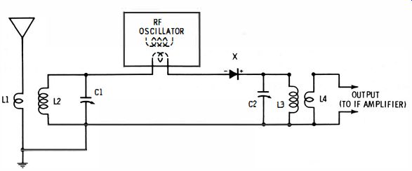
Fig. 1-16. Conventional-diode frequency converter.
The nonlinear conductance of a conventional diode enables the mixing of two signals to obtain a third by heterodyne action. This property is utilized in simple front-end converters in which a local oscillator signal is beat with an incoming signal to produce an output signal at a desired intermediate frequency. Fig. 1-16 shows the basic circuit of such a converter.
In this arrangement, C1 and L2 resonate at incoming signal frequency f1, and C2 and L3 resonate at desired intermediate frequency f3. The local oscillator generates frequency f2 of such value that f2 equals f1 - f3. The oscillator, which may be either tube, transistor, or tunnel-diode type, is shown coupled to the converter circuit by means of a low-impedance output coil, but capacitance coupling sometimes is employed. Capacitor C1 is mechanically ganged and electrically tracked with the oscillator tuning capacitor for single-control tuning, but the converter output circuit (C2-L3 ) is fixed-tuned to the intermediate frequency.
At frequencies up to 10 mhz, a general-purpose germanium diode, such as 1N34A, will be satisfactory. At higher frequencies, however, a mixer-type germanium diode should be used (for example, IN72, IN82, IN82A). At microwave frequencies (where, incidentally, the lumped-constant tuned circuits may be replaced with lines, cavities, or waveguides), special silicon point-contact mixer diodes must be used (for example, IN21A to IN21F, IN23, etc. ). Because the diode does not amplify, this circuit gives no conversion gain. Power in the IF output is provided chiefly by the local oscillator. The conversion loss may be minimized by using high-Q circuits and a good impedance match between converter and IF amplifier, and hand pick.
As an active element, the tunnel diode can amplify. In a mixer circuit, therefore, it will provide conversion gain, unlike the circuit shown in Fig. 1-16. But it requires DC power which the previous circuit does not. Inexpensive tunnel diodes will operate at frequencies up to several thousand megacycles at low noise level and with low DC input, and their two-terminal simplicity makes them attractive for converter use.
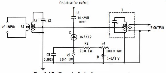
Fig. 1-17. Tunnel diode frequency converter.
Fig. 1-17 shows a typical tunnel-diode converter circuit.
Here, C1 and L2 resonate at the incoming-signal frequency.
T is a transistor-type IF transformer. The local oscillator, which may be either tube, transistor, or tunnel-diode type, is coupled to the converter circuit through capacitor C2 ; oscillator frequency f2 is chosen with respect to incoming signal frequency f1 and intermediate frequency such that f2 = f1 - f3.
By adjustment of R3, the DC operating point of the 1N3712 germanium tunnel diode (X) is set within the negative-resistance region of the diode forward conduction characteristic.
Since the diode is tapped down the primary of IF transformer T, it looks into a low impedance. If the negative resistance of the diode exceeds this impedance, however, the circuit will oscillate. Maximum gain is obtained just short of oscillation, and for this condition the resistance of R1 may require some adjustment with individual diodes.

Fig. 1-18. Varactor AFC circuit.
VARACTOR AFC CIRCUIT
The varactor is a specially processed junction diode which acts as a variable capacitor when its DC reverse voltage is varied. The DC leakage current is practically zero so that this device is essentially voltage-operated.
Fig. 1-18 shows an automatic frequency-control circuit utilizing the property of voltage-variable capacitance. Here, DC voltage from the discriminator of an FM receiver is applied to varactor C2 (V56 silicon Varicap) through an RF filter system (RFC-C3-C4-R1-R2 ). This voltage varies according to the degree of tuning of the receiver to the FM signal, and varies the capacitance of C2 proportionately. C2 is connected across the local oscillator tank through DC-blocking capacitor C1, and retunes the oscillator by an amount proportional to the DC received from the discriminator or ratio detector. Thus, drift of the local oscillator detunes the receiver from the signal and this results in a DC input signal to the AFC circuit. The DC voltage, in turn, changes the capacitance of the varactor, and this corrects the oscillator frequency to retune the receiver to the signal.
The operating point of the varactor is set by an 8-volt DC bias obtained from the receiver power supply through voltage divider R?-R4. If the power-supply output is some value other than 300 volts, resistance R4 must be proportioned accordingly to give 8 volts at the junction of C2 and R3.
VARACTOR TUNING OF RECEIVER
The voltage-variable capacitance of the varactor may be employed for the remote tuning of a radio receiver by means of a DC voltage-no DC power is required.
Fig. 1-19 shows the scheme. The conventional two-gang variable capacitor in the receiver is replaced with V-I00 Varicap silicon varactors (C3 and C4 in Fig. 1-19) . Each of these units provides a capacitance range of 57 to 260 mmf for an applied potential of zero to 15 volts DC. The local oscillator and RF (amplifier, 1st detector, or converter) stages thus are tuned simultaneously by the DC control voltage.
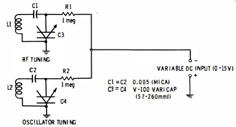
Fig. 1-19. Varactor tuning of receiver.
In each tuned circuit, a blocking capacitor (C1, C2) protects the varactor from any DC voltage that might be present in the receiver stage. The 1-megohm resistors R1 and R2 act both as RF chokes and as isolation resistors for the DC control-voltage supply. This eliminates loading of the tuned circuits by stray capacitance of the supply.
Where higher tuning capacitances are required, two or more varactors may be connected in parallel.
BIASED DIODE DETECTOR
In some instances, a small forward bias will increase the output of a detector stage employing a general-purpose germanium diode, such as a 1N34A. Since this DC voltage is applied to the diode in series with the amplitude-modulated RF voltage, it must be developed across a very low resistance, otherwise the signal will be attenuated by the DC supply.
Fig. 1-20 shows the circuit. In this arrangement, the amplitude-modulated RF signal is tuned-in by means of C1 and L2. The DC bias, variable between 13.6 and 148 millivolts by adjustment of rheostat R1, is developed across a 10-ohm resistor, R3. The AF output of diode X, together with the DC bias current flows through the primary of output transformer T. The primary of this transformer has low DC resistance to minimize attenuation of the bias current.
With a constant-amplitude RF -input signal, the AF output is measured first (with an oscilloscope or AC VTVM) with the battery disconnected and R3 temporarily short-circuited.
Then, with the short circuit removed and the battery connected, the bias is adjusted to the point at which the AF output increases over the original value. The RF input must be maintained at the same amplitude during each of these steps.
It is advisable to check the AF signal with an oscilloscope or harmonic distortion meter before and after the DC is applied, to verify that the increase in output is due to a boost in amplitude and not just to added distortion.
This is not a method of amplification. It is only a means of increasing the ratio of diode output to input by shifting operation to a more favorable point on the diode forward conduction curve. Some diodes give better performance when biased than do others of the same type; other diodes operate best without the bias.
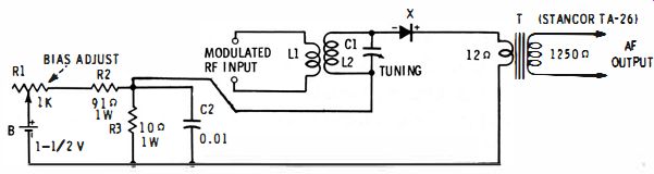
Fig. 1-20. Biased diode detector.