AMAZON multi-meters discounts AMAZON oscilloscope discounts
Semiconductor diodes may be used in various ways in radio transmitters, in auxiliary devices for transmitting stations, and in instruments for adjusting transmitters. These applications depend on the rectifying, modulating, demodulating, and distorting properties of passive diodes. Active diodes, such as the varactor and tunnel diode, perform direct transmitter circuit functions because of the ability of these units to amplify, multiply frequency, or oscillate. Active diodes often greatly simplify a circuit which otherwise would employ tubes or transistors.
ANTENNA CURRENT METER
Fig. 2-1 shows the circuit of a low-resistance radio-frequency ammeter. This instrument may be used for measuring current at frequencies of up to 200 mhz in antennas, transmission lines, and tank circuits.
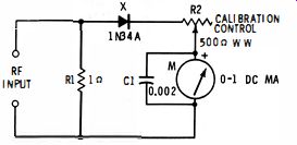
Fig. 2-1 . Antenna current meter.
RF current flows through 1-ohm noninductive resistor R1 across which it develops a voltage drop. This voltage is rectified by the IN34A germanium diode (X) , and the resulting DC deflects the 0-1 DC milliammeter (M) . Rheostat R2 serves to limit the meter current for calibration purposes, and C1 is a radio-frequency bypass capacitor.
The range Qf this instrument is 0-1 ampere rms, but higher ranges may be provided by connecting suitable non-inductive shunt resistors in parallel with the RF INPUT terminals.
To calibrate the instrument, apply an accurately known I-amp RF current to the RF Input terminals, and adjust R2 for exact full-scale deflection. Note also the reading of milliammeter M for intermediate current values, such as 0.1, 0.2, 0.3, 0.4, 0.5, 0.6, 0.7, 0.8, and 0.9 ampere. (It is necessary that this circuit be calibrated at these points, using a variable RF supply and an external RF ammeter, because of variations in diode curves and meter internal resistance.) Using these readings, prepare either a curve or chart or a special ampere scale for the meter.
NOTE: It is possible also to calibrate the meter at an audio frequency, such as 1,000 HZ, if the RF source and standard meter are not available. The final accuracy will be somewhat lower, however.
CARRIER FAILURE ALARM
When a transmitter leaves the air accidentally, the interruption can be both confusing and costly, the amount depending on the class of service supplied by the station. It is important, therefore, that the operator be alerted immediately on carrier failure.
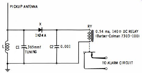
Fig. 2-2. Carrier failure alarm.
Fig. 2-2 shows the circuit of a simple carrier failure alarm.
Here, the signal is picked up with a short, vertical, whip antenna. The inductance of coil L is chosen to resonate at the signal-carrier frequency at some setting of the 365-mmf tuning capacitor (C1). The IN34A germanium diode (X) rectifies the RF signal, and the resulting DC operates the 0.54-ma, 140-ohm DC relay (RY) . As long as the signal is present, the DC keeps the relay contacts open. When the signal is interrupted, however, the DC drops to zero, and the relay contacts close, operating a bell, buzzer, light signal, or other type of alarm device in the external circuit.
This type of carrier failure alarm has the advantage of small size, excellent stability, good sensitivity, and extreme simplicity. Furthermore, it requires neither a power supply nor attended service. Being reasonably broad in response, its tuning may be left untouched for protracted periods.
CONVENTIONAL-DIODE FREQUENCY MULTIPLIER
The nonlinear conductance of the germanium diode may be utilized for frequency multiplication at low-RF power levels.
A simple passive frequency doubler, tripler, or quadrupler thus may be obtained if sufficient amplification is available for building up the signal amplitude after multiplication.
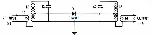
Fig. 2-3. Conventional-diode frequency multiplier.
Fig. 2-3 shows the circuit of this type of multiplier. In this arrangement, C1 and L2 are chosen to resonate at input frequency f. This frequency is to be multiplied n times by the circuit. C2 and L3 resonate at the desired higher frequency, nf. The IN281 high-conductance germanium diode is tapped across one-third of the turns of L2 and one-third of those of L3 for improved impedance match.
In adjusting the circuit, it is only necessary to tune C1 to the incoming frequency and C2 to the desired harmonic frequency. The IN281 is a 60-volt, 100-ma unit so that it will handle a respectable amount of low power.
BALANCED MODULATOR CIRCUIT
In a single-sideband transmitter, RF carrier voltage and AF modulation .voltage are presented simultaneously to a balanced modulator. Because of the circuit symmetry, the modulator suppresses the carrier and delivers an output consisting of the upper and lower sidebands (RF + AF, and RF - AF) produced by the modulation process. A bandpass filter is then used to select the desired upper or lower sideband. Balanced modulators may employ tubes, transistors, or diodes.
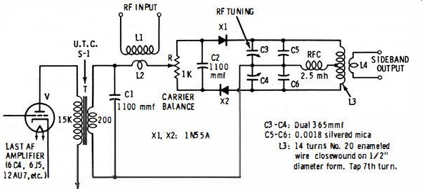
Fig. 2-4. Two-diode balanced modulator.
The diode circuit is simple, compact, and requires no power supply. It has the disadvantage that it must operate at a low power level. This is seldom inconvenient, since suitable RF amplification may be provided following the modulator, although it may not be balanced as closely as some tube circuits, even with matched diodes. However, the balance is satisfactory for amateur and experimental purposes. Diode-type balanced modulators are found in many single-sideband exciters.
Fig. 2-4 shows a popular variety of two-diode balanced modulator circuit. Here, a four-arm bridge is formed by X1, X2, top half of L3, and bottom half of L3. This bridge initially is excited by an RF voltage coupled into the circuit by L2.
Now, if the diodes were matched exactly and L3 perfectly center-tapped, the bridge would be exactly balanced and no RF output voltage would appear at L4. But since this high degree of matching is seldom obtained in practice, rheostat R is provided for correcting the circuit. When R is set to compensate for the asymmetry of the circuit, the RF output voltage is reduced to a null level very close to zero. This null holds for only one value of RF input voltage, however, because diode resistance changes with voltage. When the AF voltage is applied, the increase changes the resistance of the diodes, the bridge therefore unbalances, and RF appears at the output.
Audio frequencies cannot pass through the L3-L4 circuit. The RF energy that emerges is a combination of the upper and lower sidebands. When the AF signal ceases, the RF output again falls to zero.
In this circuit, X1 and X2 are IN55A 150-volt general purpose germanium diodes. For good balance, capacitors C5 and C6 must be matched within 1 ro, and coil L3 must be accurately center-tapped. C3 and C4 are the two sections of a dual 365-mmf variable capacitor. The C3-C4-C5-C6-L3 combination has been chosen for operation in the 75-meter amateur phone band. L1 is the RF oscillator tank coil, and L2 a 2- or 3-turn pickup coil mounted near L1. The oscillator must develop an RF signal of approximately 2.5 volts rms across L2.
Adjust the circuit initially in the following manner:
1. With the AF switched off, apply the RF signal.
2. Adjust tuning capacitor C3-C4 for maximum RF output, as indicated by peak deflection of a sensitive RF VTVM or oscilloscope at the SIDEBAND OUTPUT terminals.
3. Carefully adjust R to reduce the RF output to zero
The modulator circuit is now balanced.
4. Apply the AF signal, noting that the RF indicator deflects.
NEUTRALIZATION INDICATOR
Fig. 2-5 shows the circuit of an untuned meter-type indicator sensitive enough to show the last remnant of oscillation during the process of neutralizing a transmitter stage.
If a 1-inch meter is used, the entire instrument may be housed in a transparent plastic case or bottle to protect the operator from electric shock and may be used as a probe.
When using the instrument, coil L is held near the tank coil of the stage being neutralized. Before complete neutralization, the stage will oscillate and meter M will be deflected full scale by the DC output of rectifier diode X. As neutralization progresses, the oscillation becomes less intense and the deflection decreases proportionately, finally reaching zero when neutralization is complete.
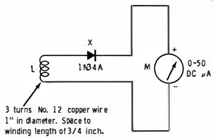
Fig. 2-5. Neutralization indicator.
TUNNEL DIODE CW TRANSMITTER
A tunnel-diode RF oscillator makes the simplest possible low-powered CW transmitter. The circuit is shown in Fig. 2-6.
Although this transmitter has an unloaded DC input of only 1.4 milliwatt, it can give surprisingly good account of itself on a clear frequency with a sensitive receiver.
The heart of the circuit is the 1N3720 germanium tunnel diode (X) . This diode will oscillate in suitable circuits at frequencies up to 0.67 kilomegacycle. In this transmitter, the oscillation frequency is determined principally by tuning capacitor C2 and plug-in coil L1. (For the amateur bands, Barker & Williamson Type JEL coils provide main coil L1 and link coupling coil L2 in each single plug-in unit. ) The RF output may be applied to an antenna through a suitable tuner or coupler.
To adjust the transmitter, connect an RF VTVM temporarily across L1. If a VTVM is not available, use an RF indicator such as the unit shown in Fig. 2-5. Depress the key and adjust R1 for peak deflection of the meter. This indicates that the DC bias has been set to the most favorable point along the negative-resistance curve of the diode. Operate the key rapidly several times to determine that oscillation starts readily when the key is depressed ; if it does not, readjust R1 for quick starting. Disconnect the VTVM and tune C2 to the desired frequency, as indicated by a frequency meter or calibrated receiver. It sometimes is necessary to reset R1 when C1 is tuned.
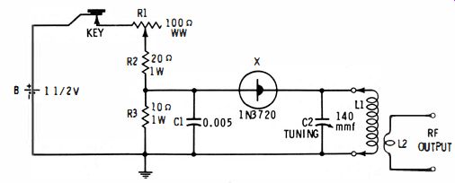
Fig. 2-6. Tunnel diode CW transmitter.
TUNNEL DIODE PHONE TRANSMITTER
The diode transmitter shown in Fig. 2-6 may be modulated by applying an AF modulating voltage in series with the DC bias, as shown in Fig. 2-7. Otherwise, the transmitter circuit is the same as that given in Fig. 2-6 and the operating instructions are the same. The RF output is frequency modulated, hence C2 and L1 should be chosen for resonance at a frequency at which FM is lawful.
Carbon microphone M receives its DC from the same 1.5 volt battery (B) that biases tunnel diode X. The bias current is adjusted by means of rheostat R2. The AF output of the microphone is superimposed upon the diode bias by transformer T. The low-impedance (16-ohm) secondary of this transformer has low DC resistance (1.4 ohms), necessary to minimize effect on the negative resistance of the diode. The amount of FM swing depends upon the AF amplitude, hence R1 acts as an FM control ; the swing is maximum when microphone output is highest. When the swing is low (narrow-band FM) , the signal may be received on an AM receiver detuned to one side of the center frequency of the signal.
Since this type of transmitter is readily sub-miniaturized, it is finding increased application as a wireless microphone and RF detectaphone.
VARACTOR AMPLITUDE MODULATOR
(A) Modulator circuit. (B) Modulator performance.
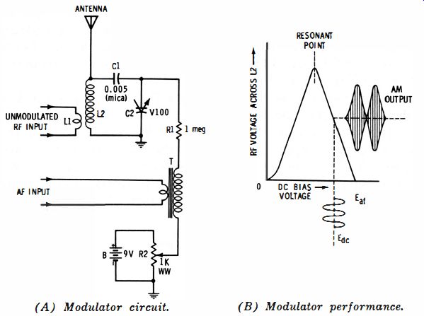
Fig. 2-8. Varactor amplitude modulator.
A low-powered CW transmitter, such as a transistorized unit, may be amplitude modulated externally by means of the varactor-tuned antenna coupler (L1-L2-C1-C2 ) (Fig. 2-8A). This coupler is tuned to the carrier frequency by V-100 Varicap C2, the capacitance of which is varied by adjusting rheostat R2 to vary the varactor DC bias. The inductance of L2 is chosen such that the circuit will resonate at the carrier frequency when the capacitance of C2 is adjusted to 80 mmf. The circuit is tuned entirely by C2 ; C1 is a blocking capacitor to keep L2 from short-circuiting the DC bias, and its reactance is negligible in the circuit. L1 is a link-coupling coil.
The AF modulation is applied in series with the DC bias, by means of transformer T which has a 2: 1 or 3: 1 stepup turns ratio. Because of the extremely high resistance of the varactor, virtually no audio power is required. An AF voltage of 1.5 volts rms should be developed across the secondary of T. The modulation voltage may be derived from a one- or two stage transistor speech amplifier or a carbon microphone.
Fig. 2-8B shows operation of the circuit. Note that the circuit is tuned to the high-frequency side of resonance by adjusting the DC bias to the level Edc (approximately -7 volts) . The AF voltage (Ear) is superimposed upon Edc' This causes the bias to swing above and below Edc at the AF rate. The resulting voltage across L2 therefore has the amplitude-modulated shape shown by the output pattern in Fig. 2-8B. For adjustment, R2 is set for best linearity of modulation, and the AF amplitude for desired percentage of modulation.
An oscilloscope, coupled to L2, serves as the monitor.
VARACTOR FREQUENCY MODULATOR
A low-powered tube or transistor oscillator stage in a transmitter may be frequency modulated by means of a varactor-tuned tank circuit. An AF voltage applied to the varactor in series with its DC bias tunes the tank above and below resonance at the AF rate, thus producing an FM output. The FM swing is proportional to the AF voltage.
Fig. 2-9 shows the circuit. The capacitance of varactor C3, a V33 Varicap, may be varied from 39 to 85 mmf by adjusting the DC bias from zero to -3 volts, by means of potentiometer R2. The inductance of L1 is chosen such that the oscillator is tuned to the desired center frequency when the varactor capacitance is set to 50 mmf. This corresponds to a DC bias of 1.5 volts and places the operating point along the steepest portion of the varactor voltage-capacitance curve. The tank circuit is isolated from the tube plate or transistor collector by capacitor C1 which blocks DC voltage coming from the tube.
Similarly, a second blocking capacitor (C2) prevents L1 from short-circuiting the varactor DC bias. L2 is a one- or two-turn link-coupled output coil.
Audio voltage is applied to the circuit through transformer T which has a 2: 1 or 3: 1 stepup turns ratio. The maximum voltage developed across the secondary of T should be between 2 and 3 volts rms. This voltage, being in series with the DC bias, swings the latter above and below the lo5-volt level at which the tank is tuned to the desired center frequency. This detunes the oscillator above and below the center frequency at the AF rate, thus producing FM output. The FM swing is proportional to the AF amplitude and may be set at a desired width by means of the audio gain control. The AF may be obtained from a transistor- or tube-type speech amplifier or directly from a carbon microphone and battery. Because of the extremely high resistance of the varactor, virtually no AF power is required.
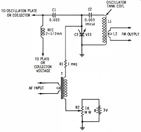
Fig. 2-9. Varactor frequency modulator.